

Page 1
General Description
The MAX4889B/MAX4889C high-speed passive switches route PCI Express®(PCIe) data between two possible destinations in desktop or notebook PCs. The
MAX4889B/MAX4889C are quad double-pole/doublethrow (4 x DPDT) switches ideal for switching four half
lanes of PCIe data between two destinations. The
MAX4889B/MAX4889C feature a single digital control
input (SEL) to switch signal paths.
The MAX4889C is intended for use in systems (e.g.,
SAS) where both the input and output are capacitively
coupled, and provides a 10µA (typ) source current and
a 60kΩ (typ) internal biasing resistor to GND at the
_OUT_ terminals.
The MAX4889B/MAX4889C are fully specified to operate from a single +3.3V (typ) power supply. Both
devices are available in an industry-standard 3.5mm x
9.0mm, 42-pin TQFN package. These devices operate
over the -40°C to +85°C extended temperature range.
Applications
Desktop PCs
Notebook PCs
Servers
Video Graphics Cards—SLI
®
(Scaled Link Interface) and CrossFire™
Features
♦ Single +3.3V Power-Supply Voltage
♦ Support PCIe Gen I, Gen II, and Gen III Data Rates
♦ Supports SAS I, SAS II, and SAS 6.0Gbps
(MAX4889C)
♦ Superior Return Loss
Better than -10dB (typ) at 5.0GHz
♦ Small 3.5mm x 9.0mm, 42-Pin TQFN Package
♦ Industry-Standard Pinouts
MAX4889B/MAX4889C
2.5/5.0/8.0Gbps PCIe Passive Switches
________________________________________________________________
Maxim Integrated Products
1
Ordering Information
19-4148; Rev 2; 8/10
For pricing, delivery, and ordering information, please contact Maxim Direct at 1-888-629-4642,
or visit Maxim’s website at www.maxim-ic.com.
+
Denotes a lead(Pb)-free/RoHS-compliant package.
*
EP = Exposed pad.
EVALUATION KIT
AVAILABLE
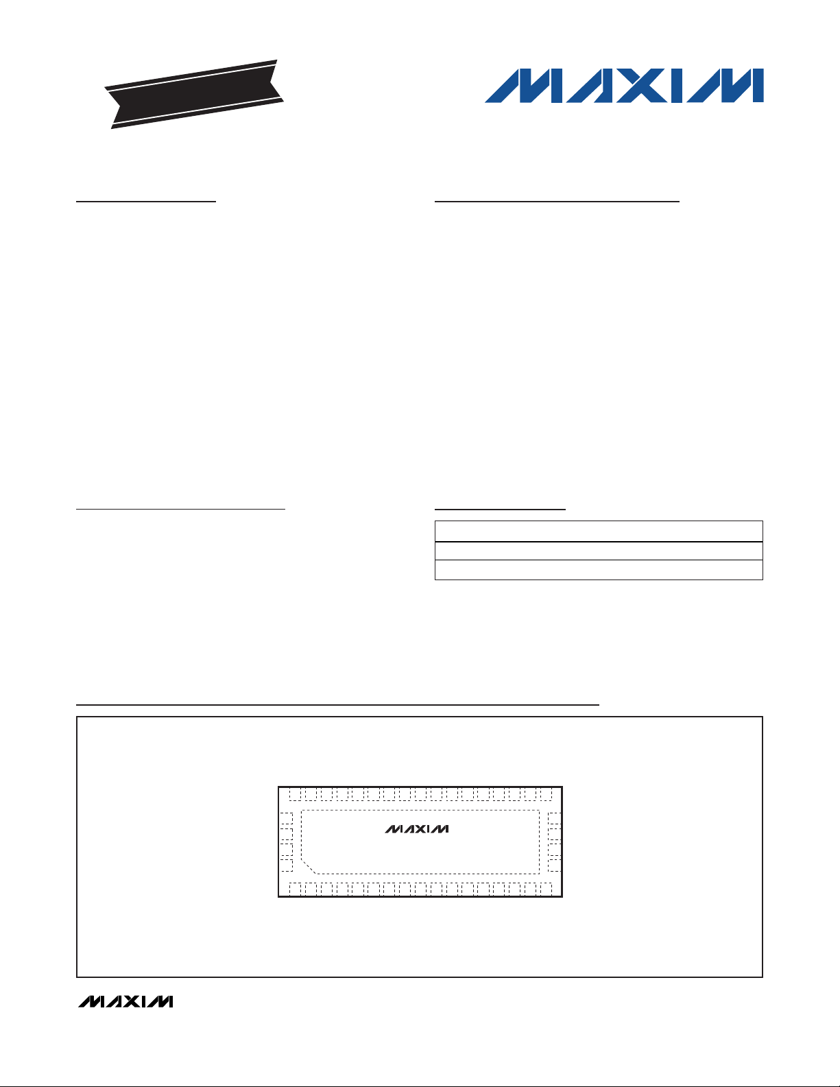
Pin Configuration
PCI Express is a registered service mark of PCI-SIG Corporation.
SLI is a registered trademark of NVIDIA Corporation.
CrossFire is a trademark of ATI Technologies, Inc.
Typical Operating Circuit appears at end of data sheet.
PART TEMP RANGE PIN-PACKAGE
MAX4889BETO+ -40°C to +85°C 42 TQFN-EP*
MAX4889CETO+ -40°C to +85°C 42 TQFN-EP*
TOP VIEW
COUTA-
VCCGND
DOUTA+
DOUTA-
DIN-
GND
21
20
19
18
DOUTB-
DOUTB+
V
CC
GND
V
CC
GND
COUTA+
GND
SEL
VCCBOUTA-
BOUTA+
VCCGND
AOUTA-
AOUTA+
GND
38 37 36 35 34 33 32 31 30 29 28 27 26 25 24 23 22
39
V
CC
40
GND
41
V
CC
GND
*CONNECT EXPOSED PAD TO GROUND.
*EP
42
+
1 2 3 4 5 6 7 8 9 1011121314151617
AIN-
AIN+
AOUTB-
AOUTB+
BIN+
BIN-
BOUTB+
MAX4889B
MAX4889C
CC
V
BOUTB-
TQFN
CIN+
CIN-
COUTB-
COUTB+
DIN+
Page 2
MAX4889B/MAX4889C
2.5/5.0/8.0Gbps PCIe Passive Switches
2 _______________________________________________________________________________________
ABSOLUTE MAXIMUM RATINGS
ELECTRICAL CHARACTERISTICS
(VCC= +3.3V ±10%, TA= T
MIN
to T
MAX,
unless otherwise noted. Typical values are at VCC= +3.3V, TA= +25°C, unless otherwise
noted.) (Note 3)
Stresses beyond those listed under “Absolute Maximum Ratings” may cause permanent damage to the device. These are stress ratings only, and functional
operation of the device at these or any other conditions beyond those indicated in the operational sections of the specifications is not implied. Exposure to
absolute maximum rating conditions for extended periods may affect device reliability.
(All voltages referenced to GND, unless otherwise noted.)
V
CC
...........................................................................-0.3V to +4V
SEL, _IN_, _OUTA_, _OUTB_ (Note 1) .......-0.3V to (V
CC
+ 0.3V)
Continuous Current (AIN_ to AOUTA_/AOUTB_, BIN_ to
BOUTA_/BOUTB_, CIN_ to COUTA_/COUTB_, DIN_ to
DOUTA_/DOUTB_) .........................................................±70mA
Peak Current (AIN_ to AOUTA_/AOUTB_, BIN_ to
BOUTA_/BOUTB_, CIN_ to COUTA_/COUTB_, DIN_ to
DOUTA_/DOUTB_)
(pulsed at 1ms, 10% duty cycle)..............................±70mA
Continuous Current (SEL).................................................±10mA
Peak Current (SEL)
(pulsed at 1ms, 10% duty cycle)..................................±10mA
Continuous Power Dissipation (T
A
= +70°C) for multilayer board:
42-Pin TQFN (derate 35.7mW/°C above +70°C) .......2857mW
Operating Temperature Range ...........................-40°C to +85°C
Junction Temperature......................................................+150°C
Storage Temperature Range .............................-65°C to +150°C
Package Junction-to-Ambient Thermal Resistance
(θ
JA
) (Note 2) ............................................................28.0°C/W
Package Junction-to-Case Thermal Resistance
(θ
JC
) (Note 2) ..............................................................2.0°C/W
Lead Temperature (soldering, 10s) .................................+300°C
Soldering Temperature (reflow) .......................................+260°C
Note 1: Signals on SEL, _IN_, _OUTA_, _OUTB_ exceeding VCCor GND are clamped by internal diodes. Limit forward-diode current
to maximum current rating.
Note 2: Package thermal resistances were obtained using the method described in JEDEC specification JESD51-7, using a four-layer
board. For detailed information on package thermal considerations, refer to www.maxim-ic.com/thermal-tutorial
.
PARAMETER SYMBOL CONDITIONS MIN TYP MAX UNITS
DC PERFORMANCE
Analog Signal Range
On-Resistance R
On-Resistance Match Between
Pairs of Same Channel
On-Resistance Match Between
Channels
On-Resistance Flatness R
_OUTA_ or _OUTB_ Off-Leakage
Current
_IN_ On-Leakage Current I
Output Short-Circuit Current
Output Open-Circuit Voltage
_IN_,
_OUTA_,
_OUTB_
ON
R
ON
R
ON
FLAT (ON)
I
_OUTA_ (OFF)
I
_OUTB_ (OFF)
_IN_ (ON)
-0.3
VCC = +3.0V, I
V
_OUTB_
VCC = +3.0V, I
V
_OUTB_
VCC = +3.0V, I
V
_OUTB_
VCC = +3.0V, I
V
_OUTB_
,
VCC = +3.6V, V
or V
_OUTB_
VCC = +3.6V, V
or V
_OUTB_
= 0V, 1.2V
= 0V (Notes 4, 5)
= 0V (Notes 4, 5)
= 0V, 1.2V (Notes 5, 6)
= 15mA, V
_IN_
= 15mA, V
_IN_
= 15mA, V
_IN_
= 15mA, V
_IN_
= 0V, 1.2V, V
_IN_
_OUTA_
_OUTA_
_OUTA_
_OUTA_
_OUTA_
= 1.2V, 0V (MAX4889B)
= 0V, 1.2V, V
= V
_IN_
or unconnected
_IN_
_OUTA_
,
,
,
,
6.4 8.4
0.1 0.5
0.2
0.3
-1 +1 μA
-1 +1 μA
V
CC
1.8
-
(MAX4889B)
All other ports are unconnected
(MAX4889C)
All other ports are unconnected
(MAX4889C)
515μA
0.2 0.6 0.9 V
V
Page 3
FREQUENCY RANGE
(GH z)
MAXIMUM INSERTION
LOS S (d B)
0–2.5
14
25
f
GHz
+0.6
2.5–5
6
5
f
GHz
-1.0
5 or greater
8
5
f
GHz
-3.0
MAX4889B/MAX4889C
2.5/5.0/8.0Gbps PCIe Passive Switches
_______________________________________________________________________________________ 3
Note 3: All units are 100% production tested at TA= +85°C. Limits over the operating temperature range are guaranteed by design
and characterization and are not production tested.
Note 4: ΔR
ON
= R
ON (MAX)
- R
ON (MIN)
.
Note 5: Guaranteed by design, not production tested.
Note 6: Flatness is defined as the difference between the maximum and minimum value of on-resistance as measured over the
specified analog signal range.
ELECTRICAL CHARACTERISTICS (continued)
(VCC= +3.3V ±10%, TA= T
MIN
to T
MAX,
unless otherwise noted. Typical values are at VCC= +3.3V, TA= +25°C, unless otherwise
noted.) (Note 3)
Table 1. Insertion Loss Mask
AC PERFORMANCE
SEL-to-Switch Turn-On Time t
SEL-to-Switch Turn-Off Time t
Propagati on Del a y tPD ZS = ZL= 50, Figure 2 50 ps
Output Skew Between Pairs t
Output Skew Between Same Pair t
Differential Return Loss (Note 5) S
Differential Insertion Loss (Note 5) S
Differential Crossta lk (Note 5) S
Differential Off-Isolation (Note 5) S
CONTROL INPUT (SEL)
Input Logic High VIH 1.4 V
Input Logic Low VIL 0.6 V
Input Logic Hysteresis V
POWER SUPPL Y
Power-Supply Range VCC 3.0 3.6 V
VCC Supply C urrent ICC V
PARAMETER SYMBOL CONDITIONS MIN TYP MAX UNITS
ZS = ZL= 50 80 ns
ON_SEL
OFF_SEL
DD21_OFF
ZS = ZL= 50, Figure 1 15 ns
ZS = ZL= 50, Figure 2 50 ps
SKEW1
ZS = ZL= 50, Figure 2 10 ps
SKEW2
0Hz < f 2.8GHz -14
DD11
DD21
DDCTK
HYST
2.8GHz < f 5.0GHz -8
f > 5.0GHz -3
See Table 1 dB
0Hz < f 2.5GHz -40
2.5GHz < f 5.0GHz -30
f > 5.0GHz -25
0Hz < f 2.5GHz -15
2.5GHz < f 5.0GHz -12
f > 5.0GHz -12
130 mV
= 0V or VCC 1 mA
SEL
dB
dB
dB
Page 4
MAX4889B/MAX4889C
2.5/5.0/8.0Gbps PCIe Passive Switches
4 _______________________________________________________________________________________
Test Circuits/Timing Diagrams
Figure 1. Switching Time
SOURCE
Z
S
Σ
SEL
V
OUT
50%
90%
t
ON_SEL
THE FREQUENCY OF THE SIGNAL SHOULD BE ABOVE THE HIGHPASS FILTER CORNER OF THE COUPLING CAPACITORS.
MAX4889B/
MAX4889C
SEL
LOAD
V
OUT
50%
10%
Z
L
t
OFF_SEL
Page 5

MAX4889B/MAX4889C
2.5/5.0/8.0Gbps PCIe Passive Switches
Test Circuits/Timing Diagrams (continued)
Figure 2. Propagation Delay and Output Skew
_______________________________________________________________________________________ 5
SOURCE
MAX4889B/
MAX4889C
Z
S
V
Σ
S+
V
V
Σ
SC+
V
SC-
V
- V
CALp
CALn
Z
S
S-
Σ
Z
S
Z
S
SEL
CALIBRATION
TRACES
Σ
50%50%
LOAD
V
OUTp
V
OUTn
V
CALp
V
CALn
Z
L
Z
L
Z
L
Z
L
V
- V
OUTp
OUTn
V
OUTp
V
OUTn
THE FREQUENCY OF THE SIGNALS SHOULD BE APPROXIMATELY 1/20 OF THE LOWEST DATA RATE.
VCM
VCM
50%50%
t
PDr
t
SK1
t
PDf
VCM
VCM
t
SK2
tPD = max (t
t
SKEW
= max (t
, t
)
PDr
PDf
, t
)
SK1
SK2
Page 6

MAX4889B/MAX4889C
2.5/5.0/8.0Gbps PCIe Passive Switches
6 _______________________________________________________________________________________
Typical Operating Characteristics
(VCC= +3.3V, TA= +25°C, unless otherwise noted.)
4.0
5.5
5.0
4.5
6.5
6.0
7.5
7.0
8.0
0 0.6 1.2 1.8
ON-RESISTANCE vs. V
_IN_
MAX4889B/9C toc01
V
_IN_
(V)
R
ON
(Ω)
VCC = +3.0V
VCC = +3.6V
VCC = +3.3V
3
2
4
5
6
7
8
9
10
0 0.3 0.6 0.9 1.2 1.5
ON-RESISTANCE vs. V
_IN_
MAX4889B/9C toc02
V
_IN_
(V)
R
ON
(Ω)
TA = +85°C
TA = -40°C TA = +25°C
250
350
300
500
450
400
650
600
550
700
-40 10-15 35 60 85
SUPPLY CURRENT
vs. TEMPERATURE
MAX4889B/9C toc03
TEMPERATURE (°C)
SUPPLY CURRENT (μA)
MAX4889B
MAX4889C
VCC = +3.6V
VCC = +3.3V
VCC = +3.0V
VCC = +3.6V
VCC = +3.3V
VCC = +3.0V
0.9
1.0
1.2
1.1
1.3
1.4
3.0 3.23.1 3.3 3.4 3.5 3.6
LOGIC THRESHOLD
vs. SUPPLY VOLTAGE
MAX4889B/9C toc04
VCC (V)
LOGIC THRESHOLD (V)
V
IH
V
IL
0
10
20
60
50
40
30
80
70
90
TURN-ON/-OFF TIME
vs. SUPPLY VOLTAGE
MAX4889B/9C toc05
VCC (V)
TURN-ON/-OFF TIME (ns)
3.0 3.4 3.53.2 3.33.1 3.6
t
ON_SEL
t
OFF_SEL
-20
-16
-18
-12
-14
-8
-10
-6
-2
-4
0
0246810
DIFFERENTIAL INSERTION LOSS
vs. FREQUENCY
MAX4889B/9C toc06
FREQUENCY (GHz)
DIFFERENTIAL INSERITON LOSS (dB)
MAX4889B
MAX4889C
MASK
-50
-40
-45
-30
-35
-20
-25
-15
-5
-10
0
0246810
DIFFERENTIAL OFF-ISOLATION
vs. FREQUENCY
MAX4889B/9C toc07
FREQUENCY (GHz)
DIFFERENTIAL OFF-ISOLATION (dB)
-80
-60
-70
-50
-20
-10
-30
-40
0
0246810
DIFFERENTIAL CROSSTALK
vs. FREQUENCY
MAX4889B/9C toc08
FREQUENCY (GHz)
DIFFERENTIAL CROSSTALK (dB)
-40
-30
-35
-25
-10
-5
-15
-20
0
0246810
DIFFERENTIAL RETURN LOSS
vs. FREQUENCY
MAX4889B/9C toc09
FREQUENCY (GHz)
DIFFERENTIAL RETURN LOSS (dB)
MAX4889B
MAX4889C
MASK
Page 7

MAX4889B/MAX4889C
2.5/5.0/8.0Gbps PCIe Passive Switches
_______________________________________________________________________________________ 7
Functional Diagram/Truth Table
AIN+
AIN-
BIN+
BIN-
V
CC
V
CC
MAX4889CMAX4889B
AOUTA+
AOUTA-
AOUTB+
AOUTB-
BOUTA+
BOUTA-
BOUTB+
BOUTB-
AIN+
AIN-
BIN+
BIN-
AOUTA+
AOUTA-
AOUTB+
AOUTB-
BOUTA+
BOUTA-
BOUTB+
BOUTB-
SEL
0 (DEFAULT)
1
_IN_ TO
_OUTA_
ON
OFF
_IN_ TO
_OUTB_
OFF
ON
CIN+
CIN-
DIN+
DIN-
CONTROL
SEL
GND
COUTA+
COUTA-
COUTB+
COUTB-
DOUTA+
DOUTA-
DOUTB+
DOUTB-
CIN+
CIN-
DIN+
DIN-
SEL
COUTA+
COUTA-
COUTB+
COUTB-
DOUTA+
DOUTA-
DOUTB+
DOUTB-
CONTROL
GND
Page 8
MAX4889B/MAX4889C
2.5/5.0/8.0Gbps PCIe Passive Switches
8 _______________________________________________________________________________________
Pin Description
PIN
MAX4889B/
MAX4889C
1 AIN+ Analog Switch 1. Common Positive Terminal.
2 AIN- Analog Switch 1. Common Negative Terminal.
3 AOUTB+ Analog Switch 1. Normally Open Positive Terminal.
4 AOUTB- Analog Switch 1. Normally Open Negative Terminal.
5 BIN+ Analog Switch 2. Common Positive Terminal.
6 BIN- Analog Switch 2. Common Negative Terminal.
7 BOUTB+ Analog Switch 2. Normally Open Positive Terminal.
8 BOUTB- Analog Switch 2. Normally Open Negative Terminal.
9, 19, 21, 26, 31,
34, 39, 41
10 CIN+ Analog Switch 3. Common Positive Terminal.
11 CIN- Analog Switch 3. Common Negative Terminal.
12 COUTB+ Analog Switch 3. Normally Open Positive Terminal.
13 COUTB- Analog Switch 3. Normally Open Negative Terminal.
14 DIN+ Analog Switch 4. Common Positive Terminal.
15 DIN- Analog Switch 4. Common Negative Terminal.
16 DOUTB+ Analog Switch 4. Normally Open Positive Terminal.
17 DOUTB- Analog Switch 4. Normally Open Negative Terminal.
18, 20, 22, 25, 29,
35, 38, 40, 42
23 DOUTA- Analog Switch 4. Normally Closed Negative Terminal.
24 DOUTA+ Analog Switch 4. Normally Closed Positive Terminal.
27 COUTA- Analog Switch 3. Normally Closed Negative Terminal.
28 COUTA+ Analog Switch 3. Normally Closed Positive Terminal.
30 SEL Control Signal Input. SEL has a 70kΩ (typ) pulldown resistor to GND.
32 BOUTA - Analog Switch 2. Normally Closed Negative Terminal.
33 BOUTA+ Analog Switch 2. Normally Closed Positive Terminal.
36 AOUTA- Analog Switch 1. Normally Closed Negative Terminal.
37 AOUTA+ Analog Switch 1. Normally Closed Positive Terminal.
— EP Exposed Pad. Connect EP to GND.
NAME FUNCTION
V
CC
GND Ground
P osi ti ve S up p l y V ol tag e Inp ut. C onnect V
a 0.1µF cer am i c cap aci tor p l aced as cl ose as p ossi b l e to the d evi ce. S ee the Boar d Layout secti on.
to a 3.0V to 3.6V sup p l y vol tag e. Byp ass V
C C
to GN D w i th
C C
Page 9

Detailed Description
The MAX4889B high-speed passive switch routes PCI
Express (PCIe) data or other high-speed signals with
amplitude of ≤ 1.2V
P-P
differential, and common-mode
voltage close to 0V between two possible destinations.
The MAX4889B is ideal for routing PCIe signals to
change system configuration. For example, in a graphics
application, four MAX4889B devices create two sets of
eight lanes from a single 16-lane bus. The MAX4889C
feature a 10µA (typ) source current and a 60kΩ (typ)
internal biasing resistor to GND at the _OUT_ terminals.
The MAX4889C is ideal for dual capacitively coupled
applications such as SAS and SATA. The MAX4889B/
MAX4889C feature a single digital control input (SEL) to
switch signal paths. SEL has a 70kΩ (typ) pulldown
resistor to GND.
The MAX4889B/MAX4889C are fully specified to operate from a single 3.0V to 3.6V power supply.
Digital Control Input (SEL)
The MAX4889B/MAX4889C provide a single digital
control input (SEL) to select the signal path between
the _IN_ and _OUT_ channels. The truth tables for the
MAX4889B/MAX4889C are illustrated in the
Functional
Diagram/Truth Table
. SEL has a 70kΩ (typ) pulldown
resistor to GND.
Analog Signal Levels
The MAX4889B/MAX4889C accept standard PCIe signals
to a maximum of (VCC- 1.8V). Signals on the _IN+ channels are routed to either the _OUTA+ or _OUTB+ channels. Signals on the _IN- channels are routed to either the
_OUTA- or _OUTB- channels. The MAX4889B/MAX4889C
are bidirectional switches, allowing _IN_ and _OUT_ to be
used as either inputs or outputs.
Applications Information
PCIe Switching
The MAX4889B/MAX4889C primary applications are
aimed at reallocating PCIe lanes (see the
Typical
Operating Circuit: Video Graphics Cards
). For example,
in graphics applications, several manufacturers have
found that it is possible to improve performance by a factor of nearly two by splitting a single 16-lane PCIe bus
into two 8-lane buses. Two of the more prominent examples are SLI (Scaled Link Interface) and CrossFire. Four
MAX4889Bs permit a computer motherboard to operate
properly with a single 16-lane graphics card, which can
later be upgraded to dual cards.
Board Layout
High-speed switches require proper layout and design
procedures for optimum performance. Keep controlledimpedance PCB traces as short as possible or follow
impedance layouts per the PCIe specification. Ensure
that power-supply bypass capacitors are placed as
close as possible to the device. Multiple bypass capacitors are recommended. Connect all grounds and the
exposed pad to large ground planes.
MAX4889B/MAX4889C
2.5/5.0/8.0Gbps PCIe Passive Switches
_______________________________________________________________________________________ 9
Page 10
MAX4889B/MAX4889C
2.5/5.0/8.0Gbps PCIe Passive Switches
10 ______________________________________________________________________________________
Typical Operating Circuit: Video Graphics Cards
CHANNEL
SELECT
PCIe
NORTH BRIDGE
SEL
LANE 0 TX
LANE 1 TX
LANE 2 TX
LANE 3 TX
AIN+
AIN-
BIN+
BIN-
CIN+
CIN-
DIN+
DIN-
MAX4889B
CHANNEL
SELECT
V
GND
V
CC
AOUTA+
AOUTA-
BOUTA+
BOUTA-
COUTA+
COUTA-
DOUTA+
DOUTA-
AOUTB+
AOUTB-
BOUTB+
BOUTB-
COUTB+
COUTB-
DOUTB+
DOUTB-
CC
PCIe GRAPHICS
CONNECTOR 1
PCIe GRAPHICS
CONNECTOR 2
AOUTA+
AOUTA-
BOUTA+
BOUTA-
COUTA+
COUTA-
DOUTA+
DOUTA-
AOUTB+
AOUTB-
BOUTB+
BOUTB-
COUTB+
COUTB-
DOUTB+
DOUTB-
LANE 0 RX
LANE 1 RX
LANE 2 RX
LANE 3 RX
SEL
AIN+
AIN-
BIN+
BIN-
CIN+
CIN-
DIN+
DIN-
MAX4889B
GND
Page 11
MAX4889B/MAX4889C
2.5/5.0/8.0Gbps PCIe Passive Switches
______________________________________________________________________________________ 11
Chip Information
PROCESS: CMOS
Package Information
For the latest package outline information and land patterns, go
to www.maxim-ic.com/packages
. Note that a “+”, “#”, or “-” in
the package code indicates RoHS status only. Package drawings may show a different suffix character, but the drawing pertains to the package regardless of RoHS status.
PACKAGE
TYPE
PACKAGE
CODE
OUTLINE
NO.
LAND
PATTERN NO.
42 TQFN T423590M+1
21-0181 90-0079
Page 12

MAX4889B/MAX4889C
2.5/5.0/8.0Gbps PCIe Passive Switches
Maxim cannot assume responsibility for use of any circuitry other than circuitry entirely embodied in a Maxim product. No circuit patent licenses are
implied. Maxim reserves the right to change the circuitry and specifications without notice at any time.
12
____________________Maxim Integrated Products, 120 San Gabriel Drive, Sunnyvale, CA 94086 408-737-7600
© 2010 Maxim Integrated Products Maxim is a registered trademark of Maxim Integrated Products, Inc.
Revision History
REVISION
NUMBER
2 8/10
REVISION
DATE
DESCRIPTION
Added 8.0Gbps PCIe passi ve switch to the tit le; added Gen III to the data rates in the
Features sect ion; changed the return lo ss in the Fe ature s sect ion to -10dB (typ) at
5.0GHz
PAGES
CHANGED
All
 Loading...