

Page 1
19-5706; Rev 0; 12/10
EVALUATION KIT
AVAILABLE
Up to 8.0Gbps Dual Passive Switches
General Description
The MAX4888B/MAX4888C dual double-pole/doublethrow (2 x DPDT), high-speed passive switches are
ideal for switching two half-lanes of PCI ExpressM (PCIe)
data between two possible destinations. These devices
feature a dual digital control input to switch signal paths.
The MAX4888C is intended for use in systems where
both the input and output are capacitively coupled (e.g.,
SAS, SATA, XAUI, and PCIe) and provides a 10FA (typ)
source current and a 60kI (typ) internal biasing resistor
to GND at the AOUT_ and BOUT_ pins.
The devices are fully specified to operate from a single
+3.3V (typ) power supply. Both devices are available
in an industry-standard 3.5mm x 5.5mm, 28-pin TQFN
package. They operate over the -40NC to +85NC extended temperature range.
Applications
Desktop PCs
Notebook PCs
Servers
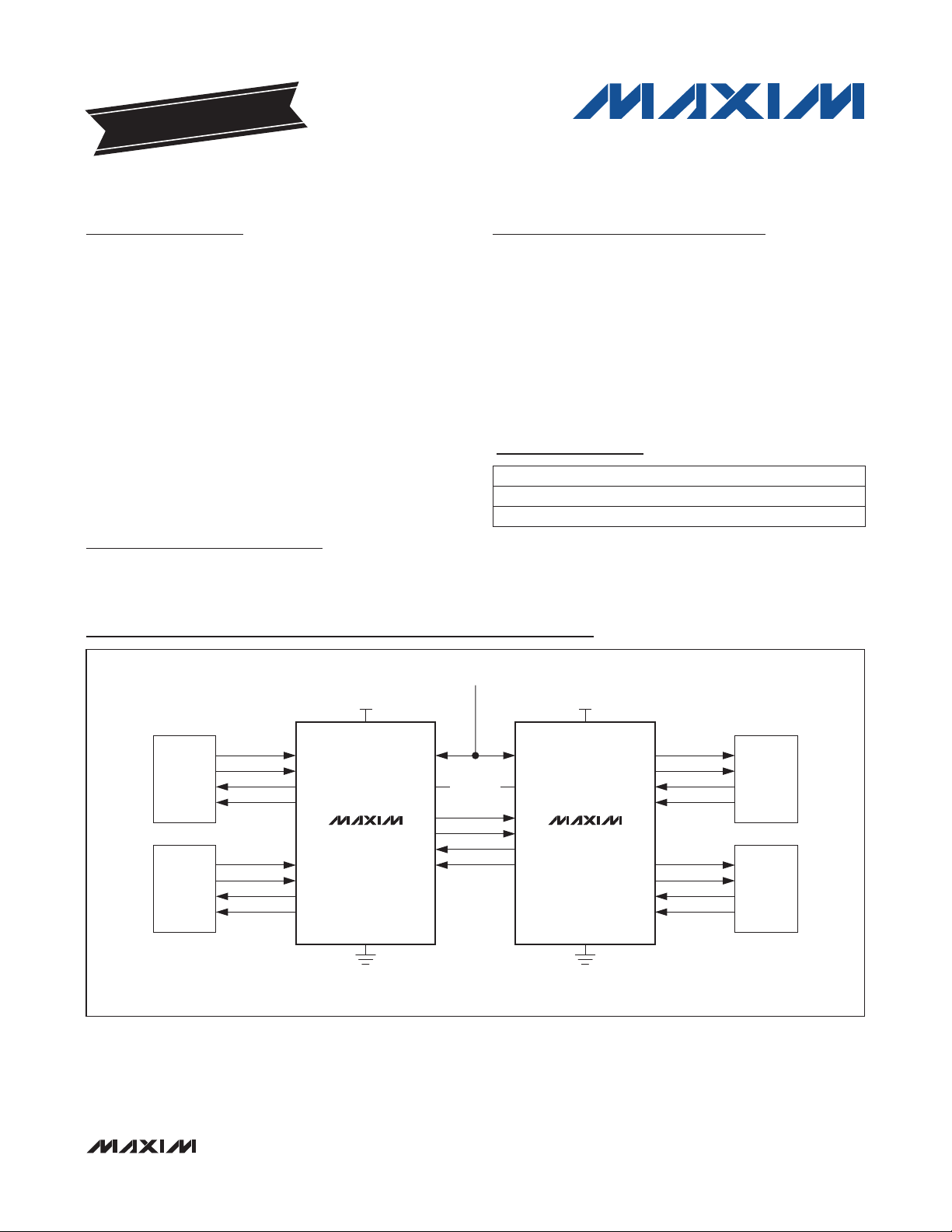
Typical Operating Circuit
Features
S Single +3.3V Power-Supply Voltage
S Supports PCIe Gen I, Gen II, and Gen III Data
Rates
S Supports Up To and Including 6.0Gbps SAS/SATA
Signals
S Supports Other High-Speed Interfaces (e.g., XAUI)
S Superior Bandwidth Return Loss
S Small, 3.5mm x 5.5mm, 28-Pin TQFN Package
Ordering Information
PART TEMP RANGE PIN-PACKAGE
MAX4888BETI+
MAX4888CETI+
-40NC to +85NC
-40NC to +85NC
+Denotes a lead(Pb)-free/RoHS-compliant package.
*EP = Exposed pad.
28 TQFN-EP*
28 TQFN-EP*
MAX4888B/MAX4888C
V
CC
AOUTA+
PCIe HOST
SAS HOST
NOTE: CAPACITIVE COUPLING WAS OMITTED TO SIMPLIFY ILLUSTRATION.
AOUTABOUTA+
BOUTA-
MAX4888C
AOUTB+
AOUTBBOUTB+
BOUTB-
GND
PCI Express is a registered trademark of PCI-SIG Corp.
CONNECTION SELECT
SEL
SELB
AIN+
AINBIN+
BIN-
SEL
SELB
AIN+
AINBIN+
BIN-
V
CC
MAX4888C
GND
AOUTA+
AOUTA-
BOUTA+
BOUTA-
AOUTB+
AOUTB-
BOUTB+
BOUTB-
PCIe DEVICE
SAS DEVICE
_______________________________________________________________ Maxim Integrated Products 1
For pricing, delivery, and ordering information, please contact Maxim Direct at 1-888-629-4642,
or visit Maxim’s website at www.maxim-ic.com.
Page 2
Up to 8.0Gbps Dual Passive Switches
ABSOLUTE MAXIMUM RATINGS
(All voltages referenced to GND, unless otherwise noted.)
VCC ..........................................................................-0.3V to +4V
SEL, SELB, AIN+, AIN-, BIN+, BIN-, AOUTA+,
AOUTA-, AOUTB+, AOUTB-, BOUTA+,
BOUTA-, BOUTB+, BOUTB- (Note 1) .. -0.3V to (VCC + 0.3V)
Continuous Current (AIN_ to AOUTA_/AOUTB_,
BIN_ to BOUTA_/BOUTB_) .......................................... Q15mA
Peak Current (AIN_ to AOUTA_/AOUTB_,
BIN_ to BOUTA_/BOUTB_)
(pulsed at 1ms, 10% duty cycle) ................................ Q70mA
Note 1: Signals on SEL, SELB, AIN_, BIN _, AOUTA_, AOUTB_, BOUTA_, and BOUTB_ exceeding VCC or GND are clamped by
internal diodes. Limit forward-diode current to maximum current rating.
PACKAGE THERMAL CHARACTERISTICS (Note 2)
TQFN
Junction-to-Ambient Thermal Resistance (qJA) ..........35°C/W
Junction-to-Case Thermal Resistance (qJC) .................2°C/W
Note 2: Package thermal resistances were obtained using the method described in JEDEC specification JESD51-7, using a four-
MAX4888B/MAX4888C
Stresses beyond those listed under “Absolute Maximum Ratings” may cause permanent damage to the device. These are stress ratings only, and functional
operation of the device at these or any other conditions beyond those indicated in the operational sections of the specifications is not implied. Exposure to absolute
maximum rating conditions for extended periods may affect device reliability.
layer board. For detailed information on package thermal considerations, refer to www.maxim-ic.com/thermal-tutorial.
Continuous Current (SEL, SELB) .................................... Q10mA
Peak Current (SEL, SELB)
(pulsed at 1ms, 10% duty cycle) ................................ Q10mA
Continuous Power Dissipation (TA = +70NC)
TQFN (derate 28.6mW/NC above +70NC)..................2286mW
Operating Temperature Range .......................... -40NC to +85NC
Junction Temperature .....................................................+150NC
Storage Temperature Range ............................ -65NC to +150NC
Lead Temperature (soldering, 10s) ................................+300NC
Soldering Temperature (reflow) ......................................+260NC
ELECTRICAL CHARACTERISTICS
(VCC = 3.3V Q10%, TA = -40NC to +85NC, unless otherwise noted. Typical values are at VCC = 3.3V, TA = +25NC, unless otherwise
noted.) (Note 3)
PARAMETER SYMBOL CONDITIONS MIN TYP MAX UNITS
DC PERFORMANCE
Analog-Signal Range V
On-Resistance R
On-Resistance Match
Between Channels
On-Resistance Flatness R
_OUTA_ or _OUTB_
Off-Leakage Current
AIN_, BIN_ On-Leakage Current
DR
FLAT(ON)
I_
OUTA_(OFF),
I_
OUTB_(OFF)
I
AIN_(ON),
I
BIN_(ON)
Output Short-Circuit Current
Output Open-Circuit Voltage
INPUT
ON
ON
AIN_, BIN_, AOUTA_, BOUTA_, AOUTB_,
BOUTB_
VCC = +3.0V, I
V_
OUTA_
= V_
VCC = +3.0V, I
V_
OUTA_
= V_
VCC = +3.0V, I
V_
OUTA_
= V_
VCC = +3.6V, V
V
_OUTA_
or V
= I
AIN_
BIN_
= 0V, 1.2V
OUTB_
= I
AIN_
BIN_
= 0V (Note 4)
OUTB_
= I
AIN_
BIN_
= 0V, 1.2V (Note 5)
OUTB_
= V
AIN_
= 1.2V, 0V
_OUTB_
= 15mA,
= 15mA,
= 15mA,
BIN_
= 0V, 1.2V;
(MAX4888B)
VCC = +3.6V , V
V
_OUTA_
or V
AIN_
_OUTB_
= V
= V
= 0V, 1.2V;
BIN_
= V
AIN_
BIN_
or
unconnected (MAX4888B)
All other ports are unconnected
(MAX4888C)
All other ports are unconnected
(MAX4888C)
-0.3
6.4 8.4
0.2 1.5
0.3 1
-1 +1
-1 +1
5 15
0.2 0.6 0.9 V
VCC -
1.8
V
I
I
I
FA
FA
FA
2
Page 3
Up to 8.0Gbps Dual Passive Switches
ELECTRICAL CHARACTERISTICS (continued)
(VCC = 3.3V Q10%, TA = -40NC to +85NC, unless otherwise noted. Typical values are at VCC = 3.3V, TA = +25NC, unless otherwise
noted.) (Note 3)
PARAMETER SYMBOL CONDITIONS MIN TYP MAX UNITS
AC PERFORMANCE
Switch Turn-On Time t
Switch Turn-Off Time t
Propagation Delay t
Output Skew Between Pairs t
Output Skew Between Same
Pair
Differential Return Loss (Note 6) S
Differential Insertion Loss S
Bandwidth S
Differential Crosstalk (Note 6) S
Differential Off-Isolation (Note 6) S
CONTROL INPUT
Input Logic-High V
Input Logic-Low V
Input Logic Hysteresis V
POWER SUPPLY
Power-Supply Range V
VCC Supply Current I
Note 3: All units are 100% production tested at TA = +85NC. Limits over the operating temperature range are guaranteed by
design and characterization and are not production tested.
Note 4: DRON = R
Note 5: Flatness is defined as the difference between the maximum and minimum value of on-resistance as measured over the
specified analog-signal range.
Note 6: Guaranteed by design; not production tested.
ON(MAX)
- R
ON(MIN)
ON_SEL
OFF_SEL
PD
SK1
t
SK2
DD11
DD21
DD12/SDD21
DDCTK
DD21_OFF
IH
IL
HYST
CC
CC
.
ZS = ZL = 50I
ZS = ZL = 50I, Figure 1, measured at
500MHz
ZS = ZL = 50I, Figure 2, measured at
500MHz
ZS = ZL = 50I, Figure 2, measured at
500MHz
ZS = ZL = 50I, Figure2
0Hz < f P 2.8GHz
2.8GHz < f P 5.0GHz
5.0GHz < f P 8.0GHz
f > 8.0GHz -1
Table 1 dB
0Hz < f P 2.5GHz
2.5GHz < f P 5.0GHz
5.0GHz < f P 8.0GHz
f > 8.0GHz -35
0Hz < f P 2.5GHz
2.5GHz < f P 5.0GHz
5.0GHz < f P 8.0GHz
f > 8.0GHz -12
-14
-8
-5
1.4 V
3.0 3.6 V
65 ns
7 ns
43 ps
8 ps
10 ps
dB
8 GHz
-30
-25
-35
-15
-12
-12
0.6 V
130 mV
1 mA
dB
dB
MAX4888B/MAX4888C
3
Page 4

Up to 8.0Gbps Dual Passive Switches
Test Circuits/Timing Diagrams
SOURCE
Z
S
Σ
SEL
MAX4888B/MAX4888C
V
OUT
t
ON_SEL
THE FREQUENCY OF THE SIGNAL SHOULD BE ABOVE THE HIGHPASS FILTER CORNER OF THE COUPLING CAPACITORS.
50%
90%
Figure 1. Switching Time
MAX4888B
MAX4888C
SEL
LOAD
V
OUT
50%
10%
Z
L
t
OFF_SEL
Table 1. Insertion Loss Mask
FREQUENCY RANGE (GHz) MAXIMUM INSERTION LOSS (dB)
0 to 2.5 1/3 x f
2.5 to 5 2/5 x f
5 to 8 18/5 x f
Greater than 8 2 x f
4
GHZ
GHZ
GHZ
GHZ
+ 17/30
- 2/5
- 4/15
- 12
Page 5

Up to 8.0Gbps Dual Passive Switches
Test Circuits/Timing Diagrams (continued)
MAX4888B/MAX4888C
V
CALp
- V
CALn
SOURCE
MAX4888B
MAX4888C
Z
S
V
Σ
S+
V
S-
V
Σ
SC+
V
SC-
Z
S
Σ
Z
S
Z
S
CALIBRATION
TRACES
SEL
Σ
LOAD
V
V
V
V
50%50%
OUTp
OUTn
CALp
CALn
Z
L
Z
L
Z
L
Z
L
V
- V
OUTp
OUTn
V
OUTp
V
OUTn
AFTER ELIMINATING SOURCE AND CABLE SKEWS.
VCM
Figure 2. Propagation Delay and Output Skew
VCM
50%50%
t
PDr
t
SK1
t
PDf
VCM
VCM
t
SK2
tPD = max (t
t
SKEW
= max (t
PDr
SK1
, t
)
PDf
, t
)
SK2
5
Page 6

Up to 8.0Gbps Dual Passive Switches
Typical Operating Characteristics
(VCC = 3.3V, TA = +25NC, unless otherwise noted.)
8.0
ON-RESISTANCE vs. V
7.5
7.0
6.5
(Ω)
6.0
ON
R
5.5
5.0
4.5
4.0
VCC = 3.3V
0 1.8
MAX4888B/MAX4888C
VCC = 3.0V
V
_IN_
LOGIC THRESHOLD
VCC = 3.6V
(V)
_IN_
10
9
MAX4888B/C toc01
8
7
(Ω)
6
ON
R
5
4
3
1.51.20.3 0.6 0.9
2
0 1.5
vs. SUPPLY VOLTAGE
1.5
1.4
1.3
1.2
1.1
LOGIC THRESHOLD (V)
1.0
0.9
0.8
V
IH
V
IL
3.0 3.6
VCC (V)
3.53.43.33.23.1
100
90
80
MAX4888B/C toc04
70
60
50
40
30
TURN-ON/OFF TIME (ns)
20
10
0
3.0 3.6
ON-RESISTANCE vs. V
TA = +85°C
TA = +25°C
TA = -40°C
V
(V)
_IN_
TURN-ON/OFF TIME
vs. SUPPLY VOLTAGE
t
ON_SEL
t
OFF_SEL
VCC (V)
_IN_
SUPPLY CURRENT vs. TEMPERATURE
350
300
MAX4888B/C toc02
250
200
SUPPLY CURRENT (µA)
150
1.20.90.3 0.6
100
MAX4888B MAX4888C
VCC = 3.6V
VCC = 3.3V
VCC = 3.0V
VCC = 3.6V
VCC = 3.3V
VCC = 3.0V
-40 85
TEMPERATURE (°C)
603510-15
MAX4888B/C toc03
DIFFERENTIAL RETURN LOSS
vs. FREQUENCY
0
-10
MAX4888B/C toc05
-20
-30
-40
-50
-60
DIFFERENTIAL RETURN LOSS (dB)
-70
3.53.43.33.23.1
-80
MASK
MAX4888B MAX4888C
0 10
FREQUENCY (GHz)
82 64
MAX4888B/C toc06
DIFFERENTIAL INSERTION LOSS
vs. FREQUENCY
0
-2
-4
-6
-8
-10
-12
-14
-16
DIFFERENTIAL INSERTION LOSS (dB)
-18
-20
MAX4888B MAX4888C
0 10
MASK
FREQUENCY (GHz)
6
DIFFERENTIAL OFF-ISOLATION
vs. FREQUENCY
0
-10
MAX4888B/C toc07
-20
-30
-40
-50
-60
DIFFERENTIAL OFF-ISOLATION (dB)
-70
862 4
-80
0 10
FREQUENCY (GHz)
82 64
-10
-20
MAX4888B/C toc08
-30
-40
-50
-60
-70
DIFFERENTIAL CROSSTALK (dB)
-80
-90
-100
DIFFERENTIAL CROSSTALK
vs. FREQUENCY
0
0 10
FREQUENCY (GHz)
862 4
MAX4888B/C toc09
Page 7

Up to 8.0Gbps Dual Passive Switches
Pin Configuration
TOP VIEW
SELB
GND
BOUTA-
BOUTA+
VCCGND
AOUTA-
AOUTA+
GND
SEL
24 23 22 21 20 19 18 17 16 15
V
*EP
BOUTB-
BOUTB+
14
13
12
11
GND
CC
GND
V
CC
GND
25
V
CC
26
GND
27
V
CC
28
GND
+
1 2 3 4 5 6 7 8 9 10
GND
AIN+
AIN-
MAX4888B
MAX4888C
AOUTB-
AOUTB+
BIN+
BIN-
TQFN
*CONNECT EXPOSED PAD TO GND.
Pin Description
PIN NAME FUNCTION
1, 10, 11,
13, 16,
20, 23,
26, 28
2 AIN+ Analog Switch 1, Common Positive Terminal
3 AIN- Analog Switch 1, Common Negative Terminal
4 AOUTB+ Analog Switch 1, Normally Open Positive Terminal
5 AOUTB- Analog Switch 1, Normally Open Negative Terminal
6 BIN+ Analog Switch 2, Common Positive Terminal
7 BIN- Analog Switch 2, Common Negative Terminal
8 BOUTB+ Analog Switch 2, Normally Open Positive Terminal
9 BOUTB- Analog Switch 2, Normally Open Negative Terminal
12, 14,
19, 25,
27
15 SELB
17 BOUTA- Analog Switch 2, Normally Closed Negative Terminal
18 BOUTA+ Analog Switch 2, Normally Closed Positive Terminal
21 AOUTA- Analog Switch 1, Normally Closed Negative Terminal
22 AOUTA+ Analog Switch 1, Normally Closed Positive Terminal
24 SEL
— EP Exposed Pad. Connect EP to GND.
GND Ground
V
CC
Positive Supply-Voltage Input. Connect V
a 0.1FF ceramic capacitor placed as close as possible to the device. See the Board Layout section.
Control Signal Input. SELB has a 70kI (typ) pullup resistor to VCC. If SELB is not in use, leave
unconnected.
Control Signal Input. SEL has a 70kI (typ) pulldown resistor to GND.
to a 3.0V to 3.6V supply voltage. Bypass VCC to GND with
CC
MAX4888B/MAX4888C
7
Page 8
Up to 8.0Gbps Dual Passive Switches
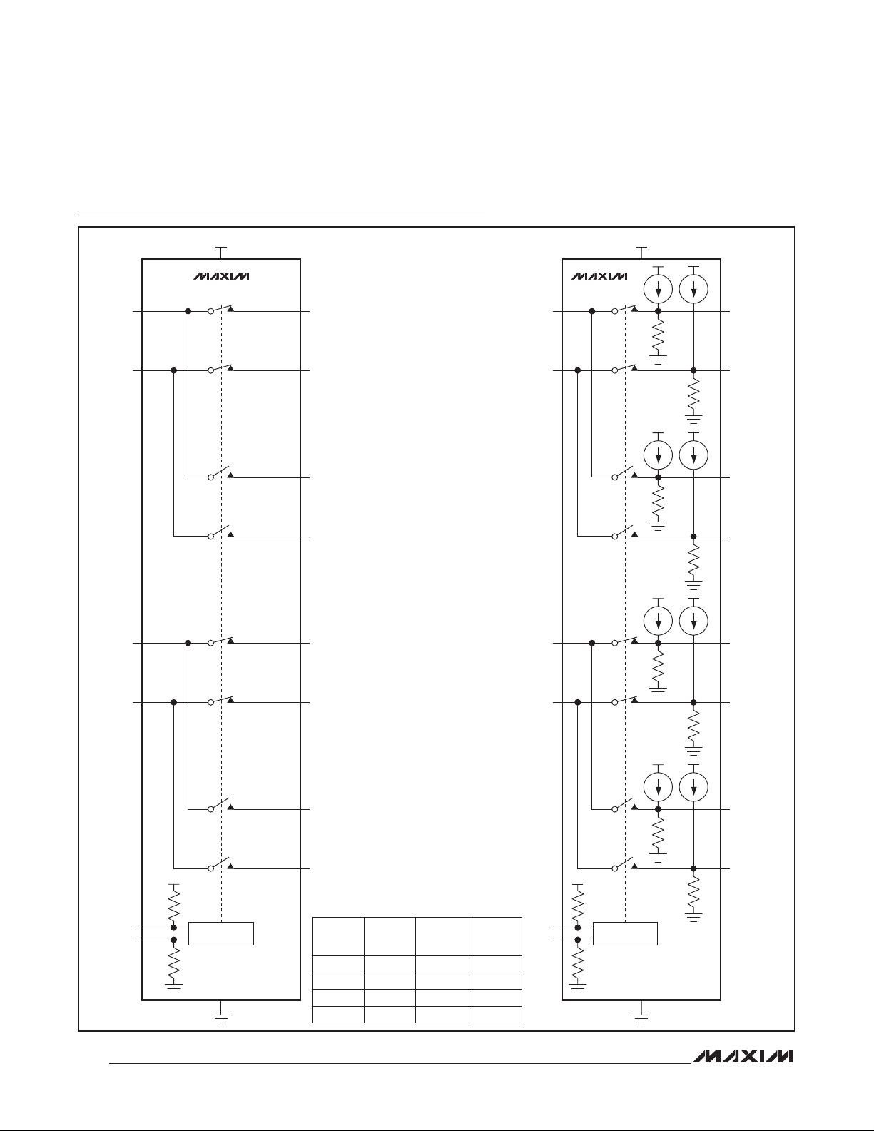
Functional Diagram/Truth Table
V
CC
MAX4888B
AOUTA+AIN+
AOUTA-AIN-
AOUTB+
MAX4888B/MAX4888C
AOUTB-
BOUTA+BIN+
MAX4888C
V
CC
AOUTA+AIN+
AOUTA-AIN-
AOUTB+
AOUTB-
BOUTA+BIN+
BOUTA-BIN-
BOUTB+
BOUTB-
SELB
SEL
BOUTA-BIN-
BOUTB+
V
CC
CONTROL
GND
BOUTB-
SEL
0 (DEFAULT)
1
0 (DEFAULT)
1
SELB
0
0
1 (DEFAULT)
1 (DEFAULT)
AIN_, BIN_
TO AOUTA_,
BOUTA_
OFF
OFF
ON
OFF
AIN_, BIN_
TO AOUTB_,
BOUTB_
ON
ON
OFF
ON
SELB
SEL
V
CC
CONTROL
GND
8
Page 9
Up to 8.0Gbps Dual Passive Switches
Detailed Description
The MAX4888B high-speed passive switch routes highspeed differential signals such as PCIe, SAS, SATA,
and XAUI from one source to two possible destinations or vice versa. The MAX4888B is ideal for routing
PCIe signals to change the system configuration. The
MAX4888C features a 10FA (typ) source current and
a 60kI (typ) internal biasing resistor to GND at the
AOUTA_, BOUTA_, AOUTB_, and BOUTB_ terminals.
The MAX4888C is ideal for circuits that are capacitively
coupled at both the output and input. These devices are
protocol independent and can be used to switch two different protocol signals over the same physical lane. They
feature dual digital control inputs (SEL, SELB) to switch
signal paths. SEL has a 70kI (typ) pulldown resistor to
GND and SELB has a 70kI (typ) pullup resistor to VCC.
These devices are fully specified to operate from a single
3.0V to 3.6V power supply.
Digital Control Input (SEL, SELB)
The devices provide dual digital control inputs (SEL,
SELB) to select the signal path between the AIN_, BIN_
and AOUTA_, BOUTA_ or AOUTB_, BOUTB_ channels. In most cases SEL is chosen and SELB is unconnected. The truth table for the devices is depicted in the
Functional Diagram/Truth Table. SEL has a 70kI (typ)
pulldown resistor to GND and SELB has a 70kI (typ)
pullup resistor to VCC.
Analog-Signal Levels
The devices accept signals from -0.3V to (VCC - 1.8V).
Signals on the AIN+ and BIN+ channels are routed to
either the AOUTA+, BOUTA+ or AOUTB+, BOUTB+
channels. Signals on the AIN- and BIN- channels are routed to either the AOUTA-, BOUTA- or AOUTB-, BOUTBchannels. The devices are bidirectional switches, allowing AIN_, BIN_ and AOUTA_, BOUTA_, AOUTB_, and
BOUTB_ to be used as either inputs or outputs.
Applications Information
High-Speed Switching
The devices’ primary applications are aimed at sharing
resources. For example, a single lane of PCIe or SAS
can be shared between a single host and two devices.
This could be used for redundancy or to share resources
such as a physical lane or route a lane between one host
and two devices or two hosts and one device.
Board Layout
High-speed switches require proper layout and design
procedures for optimum performance. Keep controlled
impedance PCB traces as short as possible or follow
impedance layouts per the PCIe specification. Ensure
that power-supply bypass capacitors are placed as
close as possible to the device. Multiple bypass capacitors are recommended. Connect all grounds and the
exposed pad to a large ground plane.
Chip Information
PROCESS: CMOS
Package Information
For the latest package outline information and land patterns,
go to www.maxim-ic.com/packages. Note that a “+”, “#”, or
“-” in the package code indicates RoHS status only. Package
drawings may show a different suffix character, but the drawing
pertains to the package regardless of RoHS status.
PACKAGE
TYPE
28 TQFN-EP T283555+1
PACKAGE
CODE
OUTLINE
NO.
21-0184 90-0123
LAND
PATTERN NO.
MAX4888B/MAX4888C
9
Page 10
Up to 8.0Gbps Dual Passive Switches
Revision History
REVISION
NUMBER
0 12/10 Initial release —
REVISION
DATE
MAX4888B/MAX4888C
DESCRIPTION
PAGES
CHANGED
Maxim cannot assume responsibility for use of any circuitry other than circuitry entirely embodied in a Maxim product. No circuit patent licenses are implied.
Maxim reserves the right to change the circuitry and specifications without notice at any time.
10 Maxim Integrated Products, 120 San Gabriel Drive, Sunnyvale, CA 94086 408-737-7600
©
2010 Maxim Integrated Products Maxim is a registered trademark of Maxim Integrated Products, Inc.
 Loading...