

Page 1
General Description
The MAX4887 triple, high-frequency switch is intended
for notebooks and monitors to permit RGB signals to be
switched from one driver to one of two loads (1:2) or one
of two sources to be connected to one load (2:1). The
MAX4887 high-performance switch utilizes n-channel
architecture with internal high-drive pullup from a lownoise charge pump, resulting in very low on-capacitance.
The MAX4887 features 5Ω (typ) on-resistance switches
with 10pF on-capacitances for routing RGB video signals. A logic input enables or disables the internal
charge pump for optimal frequency performances when
operating at lower input voltages resulting in standby
supply current less than 3µA. All RGB inputs/outputs are
ESD protected to ±8kV Human Body Model (HBM) and
feature a global input (EN) that places all inputs and outputs in a high-impedance state.
The MAX4887 is available in a small 3mm x 3mm, 16pin TQFN package for ease of assembly and
flowthrough layout, resulting in minimum space requirement and simplicity in board layout. The MAX4887
operates over the -40°C to +85°C temperature range.
Applications
Notebook Computers
Servers and Routers
Docking Stations
PC/HDTV Monitors
Features
♦ +3V/+5V Single-Supply Operation
♦ Low R
ON
5Ω (V+ = 5V)
♦ Low 10pF (typ) C
ON
♦ Global ENABLE Input to Turn On/Off Switches
♦ Break-Before-Make Switching
♦ ±8kV HBM ESD Protection per IEC1000-4-2 on I/Os
♦ Less than 1mA Supply Current (Charge Pump
Enabled)
♦ Less than 3µA Standby Mode
♦ Charge-Pump Noise Lower than 163µV
P-P
♦ Flowthrough Layout for Easy Board Layout
♦ Space-Saving Lead-Free (3mm x 3mm) 16-Pin
TQFN Package
MAX4887
Triple Video Switch
________________________________________________________________ Maxim Integrated Products 1
19-3972; Rev 0; 2/06
For pricing, delivery, and ordering information, please contact Maxim/Dallas Direct! at
1-888-629-4642, or visit Maxim’s website at www.maxim-ic.com.
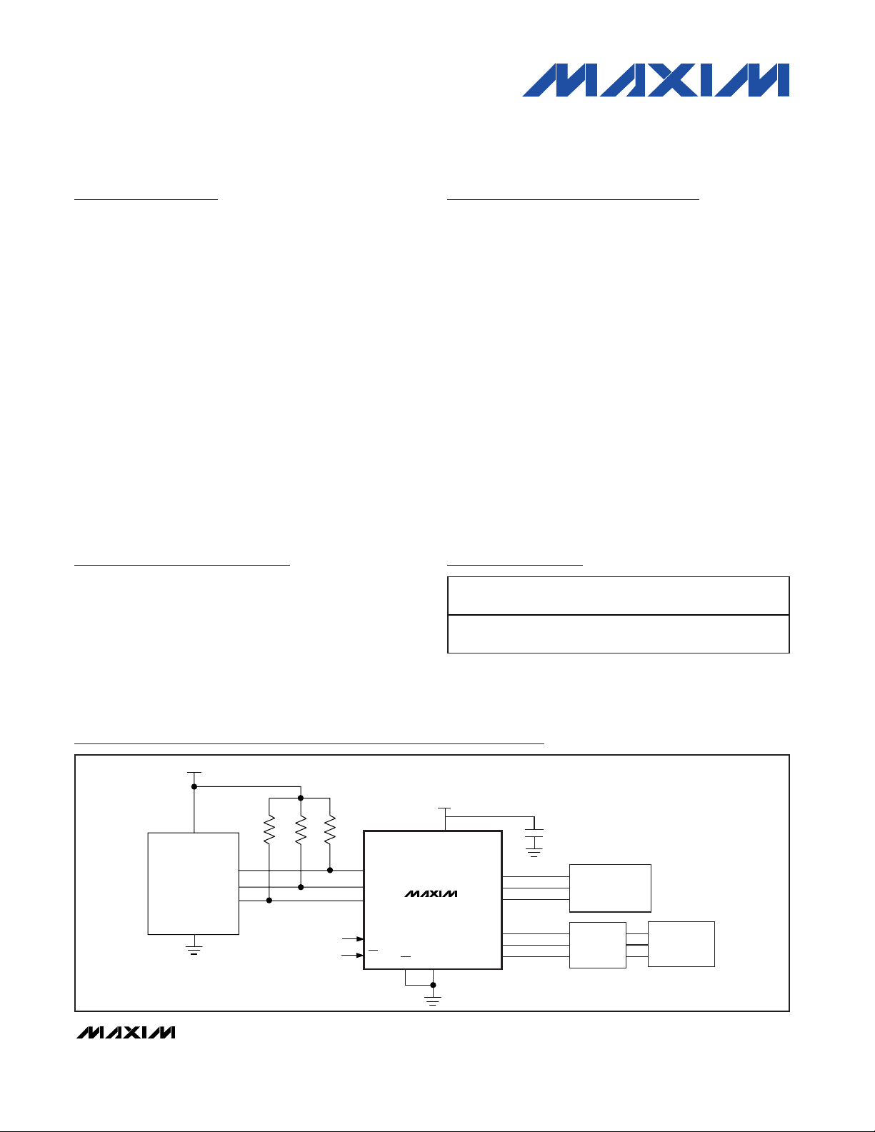
Ordering Information
VGA
D/A
CONVERTER
V
CC
V+
GND
+3.3V
+5V
EN
SEL
R0
G0
B0
0.1µF
VGA
CONNECTOR 1
DOCKING
STATION
R2
G2
B2
R1
G1
B1
QP
FROM CONTROL
SIGNALS
75Ω 75Ω
75Ω
VGA
CONNECTOR 2
MAX4887
Typical Operating Circuit
PART
TEMP
PINPACKAGE
TOP
PKG
CODE
MAX4887ETE
-40°C to
+85°C
16 TQFN-EP*
T1633-4
*EP = Exposed paddle.
The MAX4887 is available only in a lead-free package. Specify
lead-free by adding the + symbol at the end of the part number when ordering.
RANGE
3mm x 3mm
MARK
AEF
Page 2
MAX4887
Triple Video Switch
2 _______________________________________________________________________________________
ABSOLUTE MAXIMUM RATINGS
Stresses beyond those listed under “Absolute Maximum Ratings” may cause permanent damage to the device. These are stress ratings only, and functional
operation of the device at these or any other conditions beyond those indicated in the operational sections of the specifications is not implied. Exposure to
absolute maximum rating conditions for extended periods may affect device reliability.
(All voltages referenced to GND.)
V+ .............................................................................-0.3V to +6V
R_, G_, B_, SEL, QP, EN (Note 1) ................-0.3V to (V+ + 0.3V)
Continuous Current through Any Switch ........................±120mA
Peak Current through Any Switch
(pulsed at 1ms, 10% duty cycle).................................±240mA
Continuous Power Dissipation (T
A
= +70°C)
16-Pin Thin QFN-EP (derate 15.6mW/°C above
+70°C).........................................................................1250mW
Operating Temperature Range ...........................-40°C to +85°C
Storage Temperature Range .............................-65°C to +150°C
Junction Temperature......................................................+150°C
Lead Temperature (soldering, 10s) .................................+300°C
DC ELECTRICAL CHARACTERISTICS—5V SUPPLY
(V+ = 5V, QP = GND, TA= T
MIN
to T
MAX
. Typical values are at TA= +25°C, unless otherwise noted.) (Note 2)
PARAMETER
SYMBOL
CONDITIONS
MIN
TYP
MAX
UNITS
Power-Supply Voltage Range 4.5 5.5 V
QP = GND 0.5 1 mA
Quiescent Supply Current I
+
V+ = +5.5V
QP = V+ 1 3 µA
RGB SWITCHES
QP = GND 5 6.5
On-Resistance R
ON
VIN = +1.5V,
I
IN
= -25mA
QP = V+ 6 7.5
Ω
QP = GND 0.5 1.3
On-Resistance Matching ∆R
ON
0.3V < VIN < +2V,
I
IN
= -25mA (Note 3)
QP = V+ 0.7 1.5
Ω
QP = GND 0.5 1
0 < VIN < +2V,
I
IN
= -25mA
QP = V+ 0.7 1.8
On-Resistance Flatness
)
0 < VIN < +1.5V, IIN =
-25mA
QP =V+ 0.7
Ω
On-Leakage Current I
L(ON)
R_, G_, B_ = 0.7V, 4.8V; EN = GND -1 +1 µA
Off-Leakage Current I
L(OFF)
R_, G_, B_ = 0.7V, 4.8V; EN = GND
pA
LOGIC INPUTS (SEL, EN, QP)
V+ = 4.5V 0.8
Input Low Voltage V
IL
V+ = 5.5V 0.8
V
V+ = 4.5V 2.0
Input High Voltage V
IH
V+ = 5.5V 2.0
V
Input Leakage Current I
LEAK
-1 +1 µA
ESD PROTECTION
Human Body Model, R_, G_, B_ ±8
ESD Protection
Human Body Model, SEL, EN, QP ±2
kV
Note 1: Signals exceeding V+ or GND are clamped by internal diodes. Limit forward-diode current to maximum current rating.
R
FLAT(ON
300
1.55
Page 3

MAX4887
Triple Video Switch
_______________________________________________________________________________________ 3
AC ELECTRICAL CHARACTERISTICS—5V SUPPLY
(V+ = +5V, QP = GND, TA= T
MIN
to T
MAX
. Typical values are at TA= +25°C, unless otherwise noted.) (Note 2)
PARAMETER
SYMBOL
CONDITIONS
MIN
TYP
MAX
UNITS
Charge-Pump Noise V
QP
RS = RL = 50Ω
µV
P-P
Turn-On Time t
ON
VIN = +4.5V, RL = 100Ω, Figure 2 20 µs
Charge Injection
28 pC
Propagation Delay
ps
Output Skew Between Ports t
SKEW
Skew between any two ports: R, G, B;
Figure 4 (Note 3)
ps
3dB Bandwidth f
MAX
RS = RL = 50Ω, Figure 6
MHz
Off-Isolation
R
S
= RL = 50Ω, VIN_ = 1V
P-P,
f = 50MHz,
Figure 5
-58 dB
0.5
Insertion Loss I
LOS
1MHz < f < 50MHz,
R
S
= RL = 50Ω
QP = V+ 0.5
dB
Crosstalk V
CT
f < 50MHz, VIN = 1V
P-P
, RS = RL = 50Ω,
Figure 5
-40 dB
Off-Capacitance C
OFF
f = 1MHz, (R,G,B)0 to (R,G,B)
1,2
6pF
On-Capacitance C
ON
f = 1MHz 10 pF
ELECTRICAL CHARACTERISTICS—3.3V SUPPLY
(V+ = +3.3V, QP = GND, TA= T
MIN
to T
MAX
. Typical values are at TA= +25°C, unless otherwise noted.) (Note 2)
PARAMETER
SYMBOL
CONDITIONS
MIN
TYP
MAX
UNITS
Power-Supply Voltage Range 3.0 3.6 V
Quiescent Supply Current I
+
V+ = +3.6V 0.5 1 mA
RGB SWITCHES
On-Resistance R
ON
V = +3V, VIN = +1.5V, IIN = -25mA 6 7 Ω
On-Resistance Matching ∆R
ON
0 < VIN < +2V, IIN = -25mA (Note 3) 0.8 1.2 Ω
On-Resistance Flatness
)
0< VIN < +2V, IIN = -25mA 0.9 1.4 Ω
On-Leakage Current I
L(ON)
R_, G_, B_ = 0V or +3.6V, EN = GND -1 +1 µA
Off-Leakage Current I
L(OFF)
R_, G_, B_ = 0V or +3.6V, EN = V+
pA
LOGIC INPUTS (SEL, EN, QP)
V+ = 3.0V 0.8
Input Low Voltage V
IL
V+ = 3.6V 0.8
V
V+ = 3.0V 2.0
Input High Voltage V
IH
V+ = 3.6V 2.0
V
Input Leakage Current I
LEAK
-1 +1 µA
ESD PROTECTION
Human Body Model, R_, G_, B_ ±8
ESD Protection
Human Body Model, SEL, EN, QP ±2
kV
V
t
PLH/tPHLC L
= 0V , R
GE N
= 10p F, RS = RL = 50Ω , Fi g ur e 4 (Note 3) 400
= 0Ω , C L = 1.0nF, Fi g ur e 3
GE N
163
350
500
QP = GND
R
FLAT(ON
200
Page 4
MAX4887
Triple Video Switch
4 _______________________________________________________________________________________
AC ELECTRICAL CHARACTERISTICS—3.3V SUPPLY
(V+ = +3.3V, QP = GND, TA= T
MIN
to T
MAX
. Typical values are at TA= +25°C, unless otherwise noted.) (Note 2)
PARAMETER
CONDITIONS
UNITS
Charge-Pump Noise V
QP
RS = RL = 50Ω 100
µV
P-P
Turn-On Time t
ON
VIN = +3V, RL = 100Ω , Figure 2 25 µs
Charge Injection
V
GEN
= 0V, R
GEN
= 0Ω, CL = 1.0nF,
Figure 3
21 pC
Propagation Delay
C L = 10p F, RS = RL = 50Ω , Fi g ur e 4 ( N ote 3)
ps
Output Skew Between Ports t
SKEW
Skew between any two ports: R, G, B,
Figure 5 (Note 3)
ps
3dB Bandwidth f
MAX
RS = RL = 50Ω, Figure 5 500
MHz
Insertion Loss I
LOS
1MHz < f < 50MHz, RS = RL = 50Ω 0.6 dB
Crosstalk V
CT
f < 50MHz, RS = RL = 50Ω, Figure 5 -40 dB
Off-Isolation
R
S
= RL = 50Ω, VIN_ = 1V
P-P
, f = 50MHz,
Figure 5
-55 dB
Off-Capacitance C
OFF
f = 1MHz, (R,G,B)0 to (R,G,B)
1,2
6pF
On-Capacitance C
ON
f = 1MHz 10 pF
Note 2: Maximum and minimum limits over temperature are guaranteed by design and characterization. Device is production tested
at T
A
= +85°C.
Note 3: Guaranteed by design.
SYMBOL
MIN TYP MAX
t
PHL/tPLH
400
350
Page 5
MAX4887
Triple Video Switch
_______________________________________________________________________________________ 5
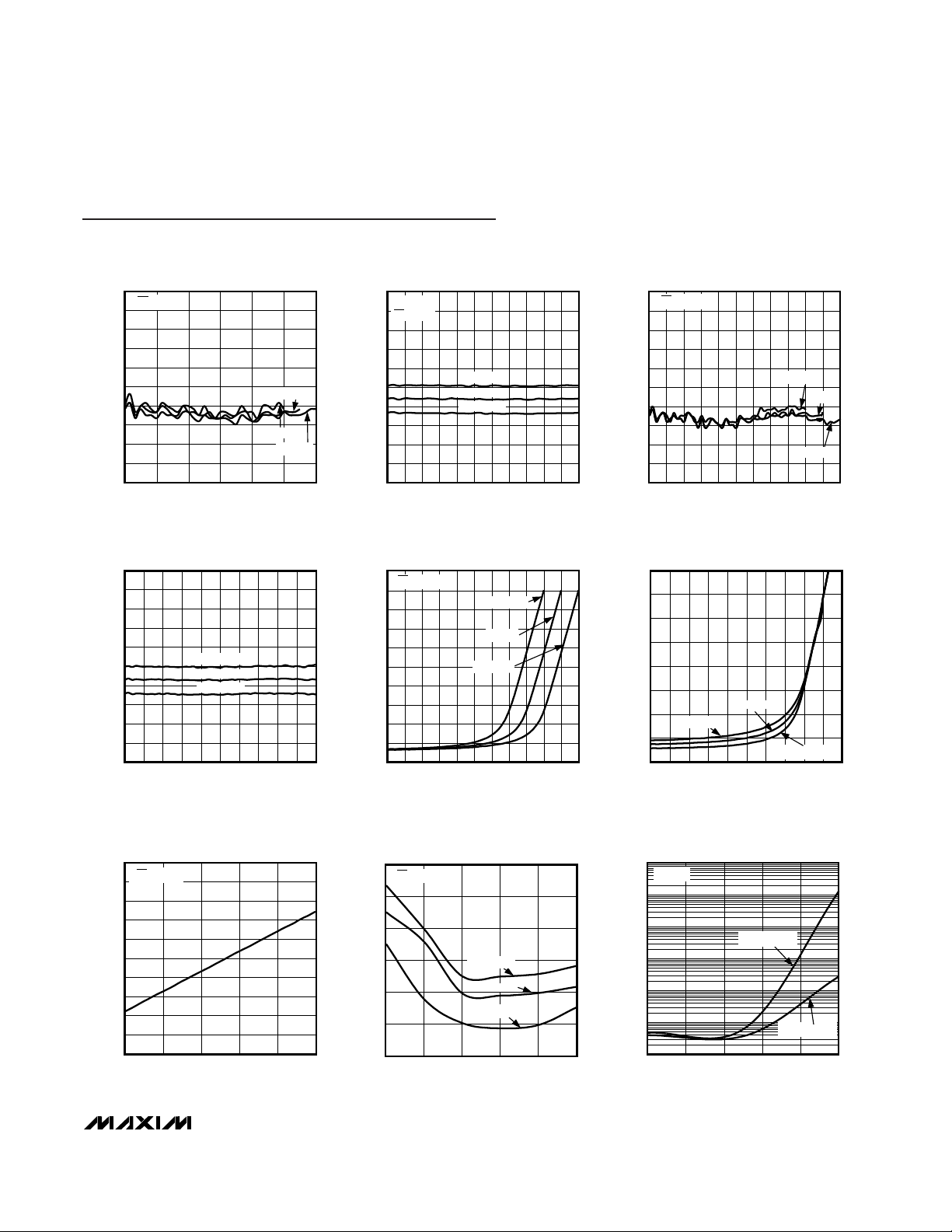
4.0
4.3
4.2
4.1
4.4
4.5
4.6
4.7
4.8
4.9
5.0
01.20.6 1.8 2.4 3.0 3.6
ON-RESISTANCE vs. V+
MAX4887 toc01
V
RGB
(V)
ON-RESISTANCE (Ω)
V+ = 3V
QP = LOW
V+ = 3.3V
V+ = 3.6V
0
2
1
5
4
3
6
7
9
8
10
00.60.90.3 1.2 1.5 1.8 2.1 2.4 2.7 3.0 3.3
ON-RESISTANCE vs. V
RGB
MAX4887 toc02
V
RGB
(V)
ON-RESISTANCE (Ω)
TA = +85°C
TA = +25°C
TA = -40°C
V+ = 3.3V
QP = LOW
4.0
4.2
4.1
4.5
4.4
4.3
4.6
4.7
4.9
4.8
5.0
01.01.50.5 2.0 2.5 3.0 3.5 4.0 4.5 5.0 5.5
ON-RESISTANCE vs. V+
MAX4887 toc03
V
RGB
(V)
ON-RESISTANCE (Ω)
QP = LOW
V+ = 5.5V
V+ = 4.5V
V+ = 5V
01.01.52.00.5 2.5 3.0 3.5 4.54.0 5.0
ON-RESISTANCE vs. V
RGB
MAX4887 toc04
V
RGB
(V)
0
2
1
5
4
3
6
7
9
8
10
ON-RESISTANCE (Ω)
TA = +85°C
TA = +25°C
TA = -40°C
0
12
6
30
24
18
36
42
54
48
60
0 1.0 1.50.5 2.0 2.5 3.0 3.5 4.0 4.5 5.0 5.5
ON-RESISTANCE vs. V+
MAX4887 toc05
V
RGB
(V)
ON-RESISTANCE (Ω)
QP = HIGH
V+ = 5.5V
V+ = 4.5V
V+ = 5V
0
10
5
15
30
35
25
20
40
0 1.0 1.5 2.0 2.50.5 3.0 3.5 4.0 4.5 5.0
ON-RESISTANCE vs. V
RGB
MAX4887 toc06
V
RGB
(V)
ON-RESISTANCE (Ω)
TA = +85°C
TA = +25°C
TA = -40°C
200
350
300
250
400
450
500
550
600
650
700
3.0 4.03.5 4.5 5.0 5.5
SUPPLY CURRENT
vs. SUPPLY VOLTAGE
MAX4887 toc07
V+ (V)
SUPPLY CURRENT (nA)
QP = HIGH
200
300
250
400
350
450
500
3.0 4.03.5 4.5 5.0 5.5
SUPPLY CURRENT
vs. SUPPLY VOLTAGE
MAX4887 toc08
V+ (V)
SUPPLY CURRENT (µA)
QP = LOW
TA = +85°C
TA = +25°C
TA = -40°C
0.001
0.1
0.01
10
1
100
1000
-40 10-15 35 60 85
RGB ON/OFF-LEAKAGE CURRENT
vs. TEMPERATURE
MAX4887 toc09
TEMPERATURE (°C)
LEAKAGE CURRENT (nA)
V+ = 5V
ON-LEAKAGE
OFF-LEAKAGE
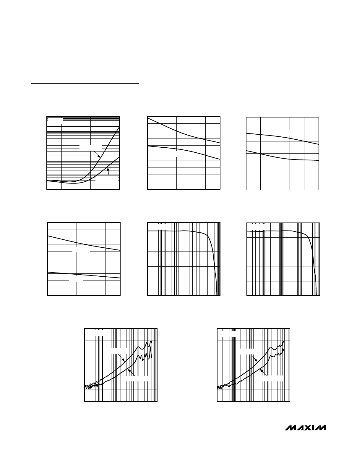
Typical Operating Characteristics
(TA = +25°C, unless otherwise noted.)
Page 6
MAX4887
Triple Video Switch
6 _______________________________________________________________________________________
0.001
0.1
0.01
10
1
100
-40 10-15 35 60 85
RGB ON/OFF-LEAKAGE CURRENT
vs. TEMPERATURE
MAX4887 toc10
TEMPERATURE (°C)
LEAKAGE CURRENT (nA)
V+ = 3.3V
ON-LEAKAGE
OFF-LEAKAGE
4.0
4.6
4.4
4.2
4.8
5.0
5.2
5.4
5.6
5.8
6.0
-40 10-15 35 60 85
TURN-ON TIMES
vs. TEMPERATURE
MAX4887 toc11
TEMPERATURE (°C)
TURN OFF TIMES (µs)
V+ = 3.3V
V+ = 5V
0
20
10
40
30
50
60
-40 10-15 35 60 85
TURN-OFF TIMES
vs. TEMPERATURE
MAX4887 toc12
TEMPERATURE (°C)
TURN-OFF TIMES (ns)
V+ = 3.3V
V+ = 5V
130
145
140
135
150
155
160
165
170
175
180
-40 10-15 35 60 85
PROPAGATION DELAY
vs. TEMPERATURE
MAX4887 toc13
TEMPERATURE (°C)
PROPAGATION DELAY (ps)
V+ = 3.3V
V+ = 5V
INSERTION LOSS
vs. FREQUENCY
MAX4887 toc14
FREQUENCY (MHz)
INSERTION LOSS (dB)
100101
-4
-3
-2
-1
0
-5
0.1 1000
V+ = 3.3V
INSERTION LOSS
vs. FREQUENCY
MAX4887 toc15
FREQUENCY (MHz)
INSERTION LOSS (dB)
100101
-4
-3
-2
-1
0
-5
0.1 1000
V+ = 5V
OFF-ISOLATION/CROSSTALK
vs. FREQUENCY
MAX4887 toc16
FREQUENCY (MHz)
OFF-ISOLATION (dB)
100101
-100
-80
-60
-40
-20
0
-120
0.1 1000
CROSSTALK
V+ = +3.3V
OFF-ISOLATION
OFF-ISOLATION/CROSSTALK
vs. FREQUENCY
MAX4887 toc17
FREQUENCY (MHz)
OFF-ISOLATION (dB)
100101
-100
-80
-60
-40
-20
0
-120
0.1 1000
CROSSTALK
V+ = +5V
OFF-ISOLATION
Typical Operating Characteristics (continued)
(TA = +25°C, unless otherwise noted.)
Page 7

Detailed Description
The MAX4887 triple, high-frequency switch is intended
for notebooks and monitors permitting RGB (red,
green, blue) signals to be switched from one driver to
one of two loads (1:2) or one of two sources to be connected to one load (2:1). The MAX4887 provides three
SPDT high-bandwidth switches to route standard VGA
R, G, and B signals (see Table 1).
A boosted gate-drive voltage is generated by an internal charge pump to enhance the performance of the
RGB switches. The MAX4887 high-performance switch
utilizes n-channel architecture with internal high-drive
pullup from a low-noise charge pump resulting in very
low on-capacitance. The RGB switches function with
reduced performance when the charge pump is disabled (V+ > 5V). The MAX4887’s global input (EN)
places all inputs/outputs in a high-impedance state,
providing rejection of all signals.
The R_, G_, and B_ analog switches are identical, and
any of the three switches can be used to route red,
green, or blue video signals. All RGB inputs/outputs are
ESD protected to ±8kV Human Body Model (HBM).
Analog Signal Levels
Analog signal inputs over the full voltage range (0 to
V+) are passed through the switch with minimal change
in on-resistance (QP = low). When QP = high, the
switches can operate within 1V of V+. The switches are
bidirectional; therefore, R_, G_, and B_ can be either
inputs or outputs.
MAX4887
Triple Video Switch
_______________________________________________________________________________________ 7
Pin Description
PIN NAME FUNCTION
1V+Supply Voltage Input. Bypass V+ to GND with a 0.1µF or larger ceramic capacitor.
2R0RGB Input/Output
3G0RGB Input/Output
4B0RGB Input/Output
5 GND Ground
6 EN
Active-Low Enable Input. Drive EN high to disable the MAX4887. All I/Os are high impedance when
the device is disabled. Drive EN low for normal operation.
7, 14 N.C. Not Internally Connected
8R1RGB Input/Output
9G1RGB Input/Output
10 B1 RGB Input/Output
11 B2 RGB Input/Output
12 G2 RGB Input/Output
13 R2 RGB Input/Output
15 SEL Select Input. Logic input for switching RGB switches (see Table 1).
16 QP
Active-Low Charge-Pump Enable. Drive QP high to disable the internal charge pump (for V+ = 5V
only). RGB switch operates with reduced performance when the charge pump is disabled. Drive QP
low for normal operation.
EP EP Exposed Pad. Connect exposed pad to ground plane.
Figure 1. Functional Diagram
R0
G0
B0
SEL
EN
SWITCH
LOGIC
CONTROL
MAX4887
CHARGE
PUMP
R1
R2
G1
G2
B1
B2
QP
Page 8

MAX4887
Charge Pump
A low-noise charge pump with internal capacitors provides a doubled voltage for driving the RGB analog
switches when operating the MAX4887 at low voltages
(V+ < 5V). The charge pump adds less than 163µV
P-P
of noise to the switches. When operating with V+ = 5V,
the charge pump can be disabled to further reduce
noise; however, the analog switch’s performance is
slightly degraded resulting in higher R
ON
and insertion
loss. Drive QP high to disable the charge pump. Drive
QP low for normal operation.
When operating the MAX4887 at 3.3V, connect QP
to GND.
Logic Inputs (EN, SEL)
The MAX4887 has two logic inputs that control the
switch configuration and on/off function. Use SEL to
switch (RGB)0to (RGB)1 or (RGB)2. Use EN to connect
the switch inputs to the outputs. Drive EN low to enable
the RGB switches inputs/outputs. Drive EN high to
place all inputs/outputs in a high-impedance state.
Table 1 illustrates the MAX4887 truth table.
Triple Video Switch
8 _______________________________________________________________________________________
tr < 5ns
tf < 5ns
50%
0V
LOGIC
INPUT
R
L
R_, G_, B_
GND
C
L
INCLUDES FIXTURE AND STRAY CAPACITANCE.
V
OUT
= V
IN (
RL
)
RL + R
ON
SWITCH
INPUT
SEL
V+
t
OFF
0V
RO, GO, BO
SWITCH
OUTPUT
0.9 x V
0UT
0.9 x V
0UT
t
ON
V
OUT
SWITCH
OUTPUT
LOGIC
INPUT
LOGIC INPUT WAVEFORMS INVERTED FOR SWITCHES
THAT HAVE THE OPPOSITE LOGIC SENSE.
V+
C
L
V+
V
OUT
V
IN
MAX4887
Figure 2. Switching Time
V
GEN
GND
C
L
V
OUT
V+
V
OUT
∆V
OUT
Q = (∆V
OUT
)(CL)
SWITCH
INPUT
ON
0V
V+
OFFOFF
SEL
V+
R
GEN
SEL
MAX4887
SWITCH
OUTPUT
LOGIC INPUT (0 TO V+)
RO, GO, BO
R_, G_, B_
Figure 3. Charge Injection
EN SEL FUNCTION
00(RGB)0 to (RGB)
1
01(RGB)0 to (RGB)
2
1XR_, B_, and G_ High Impedance
Table 1. Switch Truth Table
Timing Diagrams/Test Circuits
Page 9

Applications Information
Power-Supply Bypassing and Sequencing
Proper power-supply sequencing is recommended for
all CMOS devices. Do not exceed the absolute maximum ratings because stresses beyond the listed ratings can cause permanent damage to the device.
Always sequence V+ on first, followed by R_, G_, or B_
and the logic inputs. Bypass V+ to ground with a 0.1µF
or larger ceramic capacitor as close to the device as
possible.
Layout
High-speed switches such as the MAX4887 require
proper PC board layout for optimum performance.
Ensure that impedance-controlled PC board traces for
high-speed signals are matched in length and as short
as possible. Connect the exposed paddle to a solid
ground plane.
ESD Protection
As with all Maxim devices, ESD-protection structures
are incorporated to protect against electrostatic discharges encountered during handling and assembly on
all pins. Additionally, the MAX4887 is protected to ±8kV
Human Body Model (HBM) on all switches.
Human Body Model
Several ESD testing standards exist for measuring the
robustness of ESD structures. The ESD protection of
the MAX4887 is characterized with the Human Body
Model. Figure 6 shows the model used to simulate an
ESD event resulting from contact with the human body.
The model consists of a 100pF storage capacitor that is
charged to a high voltage, then discharged through a
1.5kΩ resistor. Figure 7 shows the current waveform
when the storage capacitor is discharged into a low
impedance.
ESD Test Conditions
ESD performance depends on a variety of conditions.
Please contact Maxim for a reliability report documenting test setup, methodology, and results.
Additional Applications Information
Figure 8 illustrates the MAX4887 being used in a laptop
in a 2:1 configuration (one of two sources connected to
a load). The switch assumes the dedicated DVD player
chip outputs R, G, B video, and the MAX4887 switches
between normal VGA graphics and the dedicated DVD
device.
MAX4887
Triple Video Switch
_______________________________________________________________________________________ 9
V+
GND
+5V
EN
SEL
R _,B_,G_
0.1µF
R_, G_,B_
QP
V
IN
R_
0.5 x V
IN
B_
t
PHL1
0.5 X V
OUT
50Ω
TRACE
10pF
0.5 x V
IN
V
IN
50Ω
TRACE
V
OUT
0.5 x V
IN
V
IN
0.5 X V
OUT
0.5 x V
IN
t
PLH2
t
PHL2
t
PLH1
R_
B_
t
SKEW
= t
PLH1
- t
PLH2
OR t
PHL1
= t
PHL2
MAX4887
Figure 4. Propagation Delay and Skew Measurement
Timing Diagrams/Test Circuits (continued)
Page 10

MAX4887
Triple Video Switch
10 ______________________________________________________________________________________
50Ω TRACE
(RGB)
0
R15
49.9Ω
R13
49.9Ω
R
0
G
0
50Ω TRACE
50Ω TRACE
50Ω TRACE
(RGB)
1,2
(RGB)
0
(RGB)
1,2
R
1
G
1
R13
49.9Ω
NETWORK
ANALYZER
50Ω TRACE
50Ω TRACE
NETWORK
ANALYZER
NETWORK
ANALYZER
NETWORK
ANALYZER
NETWORK
ANALYZER
NETWORK
ANALYZER
OFF-ISOLATION
CROSSTALK
BANDWIDTH
MAX4887
Figure 5. On-Loss, Off-Isolation, and Crosstalk
CHARGE-CURRENT-
LIMIT RESISTOR
DISCHARGE
RESISTANCE
STORAGE
CAPACITOR
C
s
100pF
R
C
1MΩ
R
D
1500Ω
HIGH-
VOLTAGE
DC
SOURCE
DEVICE
UNDER
TEST
Figure 6. Human Body ESD Test Model
V+
GND
+5V
EN
0.1µF
MAX4887
VGA
GRAPHIC
GENERATOR
DEDICATED
DVD PLAYER
CHIP
SEL
VGA
R1
G1
B1
R2
G2
B2
FROM
CONTROL LINE
QP
Figure 8. The MAX4887 Used in a 2:1 MUX Configuration
IP 100%
90%
36.8%
t
RL
TIME
t
DL
CURRENT WAVEFORM
PEAK-TO-PEAK RINGING
(NOT DRAWN TO SCALE)
I
r
10%
0
0
AMPERES
Figure 7. HBM Discharge Current Waveform
Page 11

MAX4887
Triple Video Switch
______________________________________________________________________________________ 11
(3mm x 3mm) Thin QFN
*EXPOSED PADDLE. CONNECT TO GND.
R2
16
1234
12 11 10 9
15
14
13
5
6
7
8
QP
SEL
N.C.
G2
B2
B1
G1
R0
G0
B0
GND
EN
N.C.
R1
V+
MAX4887
TOP VIEW
*EP
+
Pin Configuration
Chip Information
PROCESS: BiCMOS
Page 12

MAX4887
Triple Video Switch
Maxim cannot assume responsibility for use of any circuitry other than circuitry entirely embodied in a Maxim product. No circuit patent licenses are
implied. Maxim reserves the right to change the circuitry and specifications without notice at any time.
12 ____________________Maxim Integrated Products, 120 San Gabriel Drive, Sunnyvale, CA 94086 408-737-7600
© 2006 Maxim Integrated Products Printed USA is a registered trademark of Maxim Integrated Products, Inc.
Boblet
Package Information
(The package drawing(s) in this data sheet may not reflect the most current specifications. For the latest package outline information,
go to www.maxim-ic.com/packages
.)
12x16L QFN THIN.EPS
0.10 C 0.08 C
0.10 M C A B
D
D/2
E/2
E
A1
A2
A
E2
E2/2
L
k
e
(ND - 1) X e
(NE - 1) X e
D2
D2/2
b
L
e
L
C
L
e
C
L
L
C
L
C
PACKAGE OUTLINE
21-0136
2
1
G
8, 12, 16L THIN QFN, 3x3x0.8mm
MARKING
AAAA
EXPOSED PAD VARIATIONS
1.10
T1633-1
0.95
CODES
PKG.
T1233-1
MIN.
0.95
NOM.
1.10
D2
1.25
1.10
0.95
1.25
NOM.
1.10
MAX.
1.25
MIN.
0.95
MAX.
1.25
E2
12
N
k
A2
0.25
NE
A1
ND
0
0.20 REF
-
-
3
0.0230.05
L
e
E
0.45
2.90
b
D
A
0.20
2.90
0.70
0.50 BSC.
0.55
3.00
0.65
3.10
0.25
3.00
0.75
0.30
3.10
0.80
16
0.20 REF
0.25
-
0
4
0.02
4
-
0.05
0.50 BSC.
0.30
2.90
0.40
3.00
0.20
2.90
0.70
0.25
3.00
0.75
3.10
0.50
0.80
3.10
0.30
PKG
REF. MIN.
12L 3x3
NOM. MAX. NOM.
16L 3x3
MIN. MAX.
0.35 x 45°
PIN ID
JEDEC
WEED-1
0.35 x 45° WEED-2
T1233-3
1.10
1.25
0.95 1.10
0.35 x 45°1.25 WEED-1
0.95
T1633F-3
0.65
T1633-4
0.95
0.80
0.95
0.65
0.80
1.10
1.25
0.95
1.10
0.225 x 45°
0.95
WEED-2
0.35 x 45°
1.25
WEED-2
T1633-2
0.95
1.10
1.25
0.95
1.10
0.35 x 45°
1.25
WEED-2
NO
DOWN
BONDS
ALLOWED
YES
NO
YES
N/A
NO
PACKAGE OUTLINE
21-0136
2
2
G
8, 12, 16L THIN QFN, 3x3x0.8mm
YESWEED-11.25
1.100.95
0.35 x 45°
1.25
1.10
0.95
T1233-4
T1633FH-3
0.65
0.80
0.95
0.225 x 45°
0.65
0.80
0.95
WEED-2
N/A
NOTES:
1. DIMENSIONING & TOLERANCING CONFORM TO ASME Y14.5M-1994.
2. ALL DIMENSIONS ARE IN MILLIMETERS. ANGLES ARE IN DEGREES.
3. N IS THE TOTAL NUMBER OF TERMINALS.
4. THE TERMINAL #1 IDENTIFIER AND TERMINAL NUMBERING CONVENTION SHALL CONFORM TO
JESD 95-1 SPP-012. DETAILS OF TERMINAL #1 IDENTIFIER ARE OPTIONAL, BUT MUST BE LOCATED
WITHIN THE ZONE INDICATED. THE TERMINAL #1 IDENTIFIER MAY BE EITHER A MOLD OR
MARKED FEATURE.
5. DIMENSION b APPLIES TO METALLIZED TERMINAL AND IS MEASURED BETWEEN 0.20 mm AND 0.25 mm
FROM TERMINAL TIP.
6. ND AND NE REFER TO THE NUMBER OF TERMINALS ON EACH D AND E SIDE RESPECTIVELY.
7. DEPOPULATION IS POSSIBLE IN A SYMMETRICAL FASHION.
8. COPLANARITY APPLIES TO THE EXPOSED HEAT SINK SLUG AS WELL AS THE TERMINALS.
9. DRAWING CONFORMS TO JEDEC MO220 REVISION C.
10. MARKING IS FOR PACKAGE ORIENTATION REFERENCE ONLY.
11. NUMBER OF LEADS SHOWN ARE FOR REFERENCE ONLY.
0.25 0.30 0.35
2
0.25
0
0.20 REF
--
0.02
0.05
0.35
8
2
0.55 0.75
2.90
2.90 3.00 3.10
0.65 BSC.
3.00 3.10
8L 3x3
MIN.
0.70 0.75 0.80
NOM. MAX.
TQ833-1
1.25
0.25
0.70
0.35 x 45° NOWEEC
1.25
0.70
0.25
 Loading...