

Page 1
现货库存、技术资料、百科信息、热点资讯,精彩尽在鼎好!
General Description
The MAX4886 high-speed analog switch is ideal for
HDMI/DVI switching applications, permitting 2:1 or 1:2
switching. The MAX4886 contains four differential pairs
of 1:2 or 2:1 switches for RGB and clocking signals.
The MAX4886 connects either one monitor to one of
two digital video signals, or one HDMI/DVI source to
one of two loads (sink).
The MAX4886 set of differential switches is based on
an nFET architecture with internal charge pump for gate
overdrive. This advanced architecture results in an
extremely low capacitance and on-resistance needed
for the excellent return loss requirements for digital
switching. An efficient internal charge-pump design
offers very low quiescent current for power-sensitive
notebook designs.
The MAX4886 features 8Ω (typ) on-resistance and 2.5pF
on-capacitance switches for routing RGB and CLK video
signals. The MAX4886 is a high-frequency companion
device to the MAX4929. These two devices combined
perform the full 2:1 HDMI/DVI switching function.
The MAX4886 is available in a space-saving, 42-pin,
3.5mm x 9.0mm TQFN package and operates over the
extended -40°C to +85°C temperature range.
Applications
HDTV Monitors/Receivers
Video Projectors
Notebook Computers
Digital HDTV Switch Boxes/Tuners
Multimedia Audio/Video Switchers
Servers/Routers with DVI Interfaces
Digital Video Recorders
LVDS Switching
1000 Base-BX, Switching
Features
♦ Single +3.0V to +3.6V Power Supply
♦ Low On-Resistance (R
ON
): 8Ω (typ)
♦ Low On-Capacitance (C
ON
): 2.5pF (typ)
♦ Low Skew: 20ps (typ)
♦ 700µA Low Supply Current
♦ 2.6GHz (typ) Ultra-High Bandwidth
♦ 0.6dB (typ) Ultra-Low Insertion Loss
♦ High-Frequency Companion Device to MAX4929
♦ Use MAX4886 and MAX4929 to Form a Complete
HDMI/DVI 2:1 Switch
♦ 42-Pin, 3.5mm x 9.0mm, Space-Saving TQFN
MAX4886
Quad, High-Speed HDMI/DVI 2:1 Digital Video
Switch
________________________________________________________________ Maxim Integrated Products 1
19-0807; Rev 0; 4/07
For pricing, delivery, and ordering information, please contact Maxim/Dallas Direct! at
1-888-629-4642, or visit Maxim’s website at www.maxim-ic.com.
Ordering Information
PART TEMP RANGE
PINPACKAGE
PKG
CODE
MAX4886ETO+ -40°C to +85°C 42 TQFN-EP* T42359OM-1
+Denotes a lead-free package.
*EP = Exposed paddle.
Pin Configuration appears at end of data sheet.
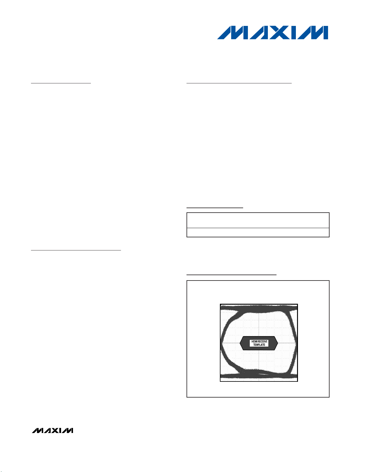
EYE DIAGRAM
(V
DD
= 3.3V, f = 2.6GHz
600mV
P-P
PRBS SIGNAL+)
* PRBS = PSUEDORANDOM BIT SEQUENCE
UI = 606ps
Eye Diagram
Page 2
MAX4886
Quad, High-Speed HDMI/DVI 2:1 Digital Video
Switch
2 _______________________________________________________________________________________
ABSOLUTE MAXIMUM RATINGS
Stresses beyond those listed under “Absolute Maximum Ratings” may cause permanent damage to the device. These are stress ratings only, and functional
operation of the device at these or any other conditions beyond those indicated in the operational sections of the specifications is not implied. Exposure to
absolute maximum rating conditions for extended periods may affect device reliability.
(All voltages referenced to GND.)
V
DD
...........................................................................-0.3V to +4V
SEL (Note 1) ...............................................-0.3V to (V
DD
+ 0.3V)
COM_, NC_, NO_ .......................................-0.3V to (V
DD
+ 0.3V)
Continuous Current Through Any Switch .......................±120mA
Peak Current Through Any Switches
(Pulsed at 1ms, 10% duty cycle).................................±240mA
Continuous Power Dissipation (T
A
= +70°C)
42-Pin Thin QFN-EP (derate 35.7mW/°C above
+70°C).....................................................................2857.1mW
Operating Temperature Range ...........................-40°C to +85°C
Storage Temperature Range .............................-65°C to +150°C
Junction Temperature .................................................... +150°C
Lead Temperature (soldering, 10s) .................................+300°C
ELECTRICAL CHARACTERISTICS
(VDD= +3.0V to +3.6V, TA= T
MIN
to T
MAX
. Typical values are at VDD= +3.3V, TA= +25°C, unless otherwise noted.) (Note 2)
PARAMETER SYMBOL CONDITIONS MIN TYP MAX UNITS
Supply Voltage Range V
DD
3.0 3.6 V
Quiescent Supply Current I
DD
+3V ≤ VDD≤ +3.6V; SEL = 0V or V
DD
600 1100 µA
ANALOG SWITCH
TA = +25°C 8 11
VDD = +3V, 0V ≤ V
COM_
≤ VDD, I
COM_
= -40mA
T
A
= T
MIN
to
T
MAX
15
TA = +25°C 8 11
On-Resistance (Note 3) R
ON
VDD = +3V,
I
COM_
= -40mA,
0 ≤ V
COM_
≤ 1.5V
T
A
= T
MIN
to
T
MAX
15
Ω
TA = +25°C 0.28 0.40
VDD = +3V, 1.5V
≤ V
COM_
≤ VDD,
I
COM_
= -40mA
T
A
= T
MIN
to
T
MAX
0.8
TA = +25°C 0.28 0.40
On-Resistance Matching
(Notes 3, 4)
ΔR
ON
VDD = +3V, 0 ≤ V
COM_
≤ 1.5V, I
COM_
= -40mA
T
A
= T
MIN
to
T
MAX
0.8
Ω
TA = +25°C 0.02 0.60
VDD = +3V,
I
COM_
= -40mA,
1.5V < V
COM_
< V
DD
TA = T
MIN
to
T
MAX
1
TA = +25°C 0.02 0.60
On-Resistance Flatness
(Note 3)
R
FLAT(ON
)
VDD = +3V,
I
COM_
= -40mA,
0 ≤ V
COM_
≤ 1.5V
T
A
= T
MIN
to
T
MAX
1
Ω
Leakage Current I
L
VDD = +3.6V, V
COM_
= +0.3V, +3.3V,
V
NC_
or V
NO_
= +3.3V, 0.3V
-1 +1 µA
SWITCH DYNAMIC
Off-Capacitance C
OFF
f = 1MHz, V
COM_
= V
NC_
or V
NO_
1.5 pF
Note 1: Signal exceeding VDDor GND are clamped by internal diodes. Limit forward-diode current to maximum current rating.
Page 3
MAX4886
Quad, High-Speed HDMI/DVI 2:1 Digital Video
Switch
_______________________________________________________________________________________ 3
ELECTRICAL CHARACTERISTICS (continued)
(VDD= +3.0V to +3.6V, TA= T
MIN
to T
MAX
. Typical values are at VDD= +3.3V, TA= +25°C, unless otherwise noted.) (Note 2)
Note 2: Maximum and minimum limits over temperature are guaranteed by design and characterization. Device is production tested
at T
A
= +25°C.
Note 3: Negative current is going into COM_ and out of NO_ or NC_.
Note 4: Guaranteed by design.
PARAMETER SYMBOL CONDITIONS MIN TYP MAX UNITS
On-Capacitance C
ON
f = 1MHz, V
COM_
= V
NC_
or V
NO_
2.5 pF
Propagation Delay t
PD1
,
t
PD2RS
= RL = 50Ω (Figure 2) 100 ps
Output Skew Between Ports t
SKEW1
Skew between any two ports, RS = RL =
50Ω (Figure 3)
20 ps
Skew Between Same Ports t
SKEW2
RS = RL = 50Ω, skew between any two
ports (Figure 3)
20 ps
SWITCH AC PERFORMANCE
On-Channel -3dB Bandwidth BW RS = RL= 50Ω (Figure 4) 2.6 GHz
Insertion Loss I
LOS
RS = RL = 50Ω, f = 50M Hz ( Fi gur e 4) 0.6 dB
Off-Isolation V
ISO
RS = RL = 50Ω, single-ended, f = 50MHz
(Figure 4)
-58 dB
Crosstalk V
CT1
Crosstalk between any two switches,
R
S
= RL = 50Ω, f = 50MHz (Figure 4)
-49 dB
LOGIC INPUTS (SEL)
Input-Low Voltage V
IL
VDD = +3.0V 0.8 V
Input-High Voltage V
IH
VDD = +3.6V 2.0 V
Input-Voltage Hysteresis V
HYST
100 mV
Input Leakage Current I
LEAK
VDD = +3.6V, V
COM_
or V
NC_
or V
NO_
= 0V -1 +1 µA
Page 4
MAX4886
Quad, High-Speed HDMI/DVI 2:1 Digital Video
Switch
4 _______________________________________________________________________________________
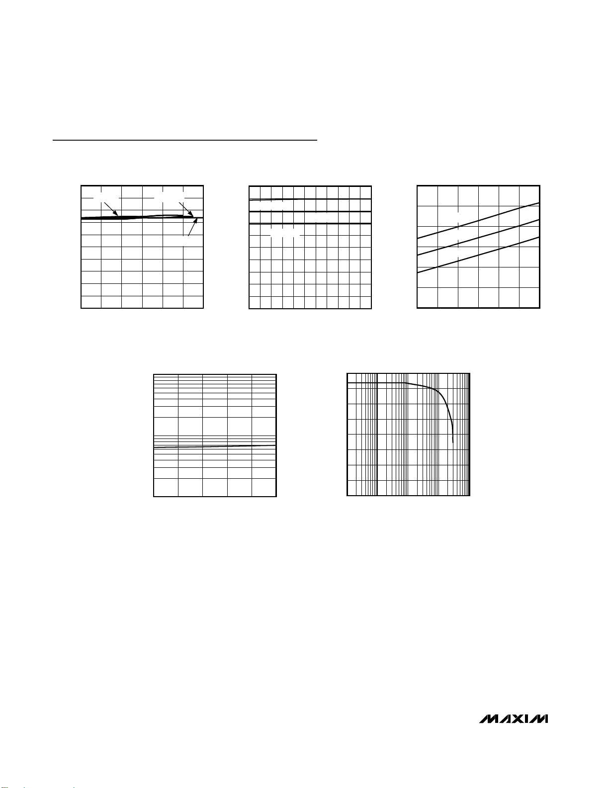
Typical Operating Characteristics
(TA = +25°C, unless otherwise noted.)
1 10 1000100 10,000
FREQUENCY RESPONSE
FREQUENCY (MHz)
ON-LOSS (dB)
0
-8
-1
-2
-3
-4
-5
-6
-7
MAX4886 toc05
LEAKAGE CURRENT vs. TEMPERATURE
TEMPERATURE (°C)
LEAKAGE CURRENT (nA)
MAX4886 toc04
-40 -15 10 35 60 85
0.1
1
10
ON-RESISTANCE vs. V
COM_
V
COM_
(V)
ON-RESISTANCE (Ω)
MAX4886 toc01
0 0.6 1.2 1.8 2.4 3.0 3.6
7.2
7.3
7.4
7.5
7.6
7.7
7.8
7.9
8.0
8.1
8.2
VDD = 3.6V
VDD = 3V
VDD = 3.3V
ON-RESISTANCE vs. TEMPERATURE
V
COM_
(V)
ON-RESISTANCE (Ω)
MAX4886 toc02
0 0.3 0.6 0.9 1.2 1.5 1.8 2.1 2.4 2.7 3.0 3.3
0
1
2
3
4
5
6
7
8
9
10
TA = -40°C
TA = +85°C
TA = +25°C
SUPPLY CURRENT vs. SUPPLY VOLTAGE
VDD (V)
SUPPLY CURRENT (μA)
MAX4886 toc03
3.0 3.1 3.2 3.3 3.4 3.5 3.6
400
450
500
550
600
650
700
TA = +25°C
TA = +85°C
TA = -40°C
Page 5
MAX4886
Quad, High-Speed HDMI/DVI 2:1 Digital Video
Switch
_______________________________________________________________________________________ 5
Pin Description
PIN NAME FUNCTION
1, 4, 10, 14,
17, 19, 21,
39, 41
GND Ground
5, 8, 13, 18,
20, 30, 40,
42
V
DD
Power-Supply Voltage Input. Bypass VDD to GND with a 0.1μF or larger ceramic capacitor.
2 COM1+ Data Signal Inputs/Outputs
3 COM1- Data Signal Inputs/Outputs
6 COM2+ Data Signal Inputs/Outputs
7 COM2- Data Signal Inputs/Outputs
9 SEL Select Input. Logic input for switch connection (see Table 1).
11 COM3+ Data Signal Inputs/Outputs
12 COM3- Data Signal Inputs/Outputs
15 COM4+ Data Signal Inputs/Outputs
16 COM4- Data Signal Inputs/Outputs
22 NO4- Differential Pair. Data Signal Inputs/Outputs.
23 NO4+ Differential Pair. Data Signal Inputs/Outputs.
24 NO3- Differential Pair. Data Signal Inputs/Outputs.
25 NO3+ Differential Pair. Data Signal Inputs/Outputs.
26 NC4- Different ia l Pair. Data Signal Inputs/Outputs.
27 NC4+ Differential Pair. Data Signal Input s/Outputs.
28 NC3- Different ia l Pair. Data Signal Inputs/Outputs.
29 NC3+ Differential Pair. Data Signal Input s/Outputs.
31 NO2- Differential Pair. Data Signal Inputs/Outputs.
32 NO2+ Differential Pair. Data Signal Inputs/Outputs.
33 NO1- Differential Pair. Data Signal Inputs/Outputs.
34 NO1+ Differential Pair. Data Signal Inputs/Outputs.
35 NC2- Different ia l Pair. Data Signal Inputs/Outputs.
36 NC2+ Differential Pair. Data Signal Input s/Outputs.
37 NC1- Different ia l Pair. Data Signal Inputs/Outputs.
38 NC1+ Differential Pair. Data Signal Input s/Outputs.
EP EP Exposed Paddle. Connect EP to GND.
Page 6

MAX4886
Detailed Description
The MAX4886 high-speed analog switch is ideal for
HDMI/DVI switching applications, permitting 2:1 or 1:2
switching. The MAX4886 contains four differential pairs
for HDMI or DVI switching. The MAX4886 connects either
one monitor to one of two digital video signals or one
HDMI/DVI output to one of two connectors or loads.
The MAX4886 differential switches are based on an
nFET architecture with an internal charge pump for gate
overdrive. This advanced architecture results in an
extremely low capacitance and on-resistance needed
for an excellent returns loss.
The MAX4886 features an 8Ω (typ) on-resistance and
2.5pF on-capacitance switches for routing RGB and
CLK video signals.
The MAX4886 switches are identical, and any of the
switches can be used to route RGB and CLK video
signals.
The device will also be useful in other high-speed
switching applications such as LVDS and LVPECL.
Analog-Signal Levels
Signal inputs over the full voltage range (0V to VDD) are
passed through the switch with minimal change in onresistance (see the Typical Operating Characteristics
section). The switches are bidirectional. Therefore,
COM_, NC_, and NO_ can be either inputs or outputs.
Logic Inputs (SEL)
The MAX4886 has a logic input that controls the switch
on/off function. Use SEL to switch COM_ to NO_ or
COM_ to NC_. Table 1 and the Functional Diagram
illustrate the MAX4886 Truth Table.
Applications Information
Power-Supply Bypassing and Sequencing
Proper power-supply sequencing is recommended for
all CMOS devices. Do not exceed the absolute
maximum ratings, because stresses beyond the listed
ratings can cause permanent damage to the device.
Always sequence V
DD
on first, followed by the switch
inputs and the logic inputs. Bypass at least one V
DD
input to ground with a 0.1µF capacitor as close to the
device as possible. Use the smallest physical size possible for optimal performance.
It is also recommended to bypass more than one V
DD
input. A good strategy is to bypass one VDDinput with
a 0.1µF capacitor and at least a second VDDinput with
a 1nF to 10nF capacitor. (Use 0603 or smaller physical
size ceramic capacitor).
PC Board (PCB) Layout
High-speed switches such as the MAX4886 require
proper PCB layout for optimum performance. Ensure
that impedance-controlled PCB traces for high-speed
signals are matched in length, and as short as possible. Connect the MAX4886 exposed paddle to a solid
ground plane.
Quad, High-Speed HDMI/DVI 2:1 Digital Video
Switch
6 _______________________________________________________________________________________
NC1+
NC1+
NO1+
NO1-
NC2+
NC2-
NO2+
NO2-
NO4+
NO4-
NC4+
NC4-
NO3+
NO3-
NC3+
NC3-
COM1+
COM1-
COM2+
COM2-
COM3+
COM3-
COM4+
COM4-
MAX4886
SEL
V
DD
GND
Table 1. Switch Truth Table
Functional Diagram
SEL FUNCTION
0 COM_ to NC_
1 COM_ to NO_
Page 7

MAX4886
Quad, High-Speed HDMI/DVI 2:1 Digital Video
Switch
_______________________________________________________________________________________ 7
LOGIC
INPUT
R
L
COM_
GND
SEL
C
L
INCLUDES FIXTURE AND STRAY CAPACITANCE.
V
OUT
= V
N_ (
R
L
)
RL + R
ON
V
N_
NC_
OR NO_
V
DD
C
L
V
DD
V
OUT
MAX4886
Figure 1. Switching Time
50Ω TRACE
COM1+
NC1+
50Ω TRACE
COM1- NC1-
IN+
IN-
OUT+
OUT-
V
DD
t
PD1
t
PD2
SEL
GND
+3.3V
COM1+
COM1-
NC1+
NC1-
IN+
IN-
OUT+
OUT-
50Ω TRACE
50Ω TRACE
MAX4886
Figure 2. Propagation Delay
Timing Circuits/Timing Diagrams
Page 8
MAX4886
Additional Applications
Information
In a typical application (see Figure 5), the MAX4886
and MAX4929 are used to route the TMDS signals and
low-frequency signals between two HDMI inputs.
In another application (see Figure 6), the MAX4886 is
used in a notebook to route high-frequency DVI port on
the computer or to the connector on the docking station. The MAX4886 routes four differential signals (RGB
and CLK) either to the DVI connector or to the docking
station port. The switch is inherently bilateral and may
be used as a 2:1 or 1:2 mux without penalties.
Quad, High-Speed HDMI/DVI 2:1 Digital Video
Switch
8 _______________________________________________________________________________________
Timing Circuits/Timing Diagrams (continued)
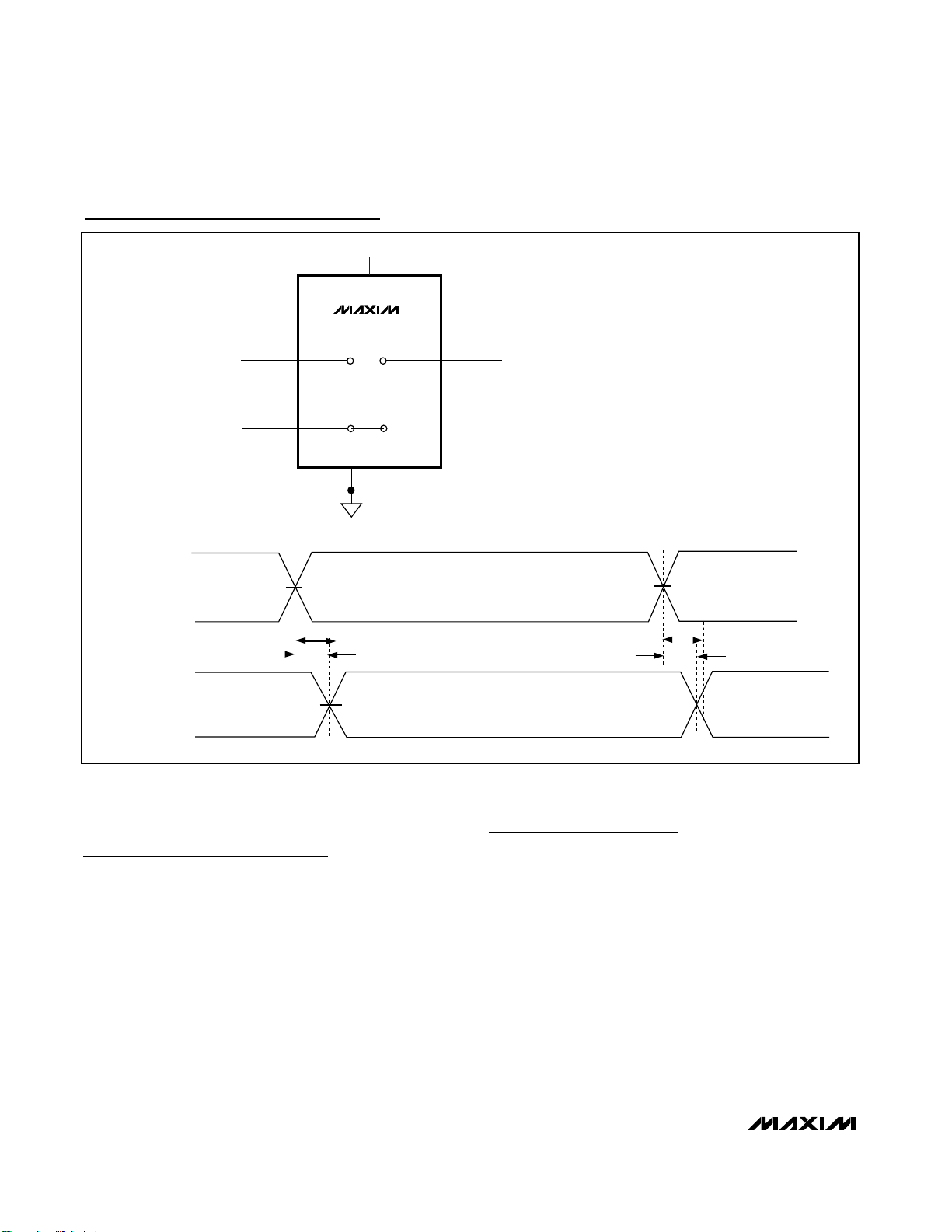
50Ω TRACE
COM1+
NC1+
50Ω TRACE
COM1- NC1-
IN+
IN-
OUT+
OUT-
V
DD
SEL
V
DD
+3.3V
COM1+
COM1-
NC1+
NC1-
IN+
IN-
OUT+
OUT-
50Ω TRACE
50Ω TRACE
MAX4886
t
PLH2
t
PLH1
50%
50%
t
PLH2
t
PLH1
50%
50%
Figure 3. Skew Measurements
Chip Information
PROCESS: BiCMOS
Connect exposed paddle to GND.
Page 9

MAX4886
Quad, High-Speed HDMI/DVI 2:1 Digital Video
Switch
_______________________________________________________________________________________ 9
Timing Circuits/Timing Diagrams (continued)
R15
49.9Ω
NETWORK
ANALYZER
NETWORK
ANALYZER
NETWORK
ANALYZER
NETWORK
ANALYZER
3dB BANDWIDTH/INSERTION LOSS
50Ω TRACE
CROSSTALK
50Ω TRACE
OFF-ISOLATION
50Ω TRACE
50Ω TRACE
COM1+
2
COM2+
6
COM2-
7
COM3+
11
NC3+
29
NC2-
35
NC2+
36
NC1+
38
50Ω TRACE
NETWORK
ANALYZER
NETWORK
ANALYZER
50Ω TRACE
R14
49.9Ω
R13
49.9Ω
MAX4886
Figure 4. On-Loss, Off-Isolation, and Crosstalk
MAX4886
MAX4929
HDMI1
TMDS
LOW-FREQUENCY SIGNALS
5V (HPIR), HPD,
DDC/SCL, DDC/SDA
NC_
R
G
B
CK
HPIR
HPD
SEL
COM_+
TMDS R
X
MCU
EDID
EEPROM
COM_-
NC_
8
8
TMDS
HDMI2
Figure 5. TV/Monitor Application
Typical Application Diagrams
Page 10

MAX4886
Quad, High-Speed HDMI/DVI 2:1 Digital Video
Switch
10 ______________________________________________________________________________________
COM1+
COM1-
COM2+
COM2-
COM3+
COM3-
COM4+
COM4-
SEL_DOCK
NO4+
NO4-
NO3+
NO3-
NO2+
NO2-
NO1+
NO1-
NC1+
NCI-
NC2+
NC2-
NC3+
NC3-
NC4+
NC4-
SEL
DVI
CONNECTOR
MONITOR
DVI
SIGNALS
DOCKING STATION
MAX4886
Figure 6. Notebook Application
Typical Application Diagrams (continued)
TOP VIEW
MAX4886
TQFN
18
19
20
21
V
DD
GND
V
DD
GND
42
+
41
40
39
V
DD
GND
V
DD
GND
1234567891011121314151617
38 37 36 35 34 33 32 31 30 29 28 27 26 25 24 23 22
COM3-
V
DD
GND
COM4+
COM4-
GND
COM3+
GND
SEL
V
DD
COM2-
COM2+
V
DD
GND
COM1-
COM1+
GND
NC4+
NC4-
NO3+
NO3-
NO4+
NO4-
NC3-
NC3+
VDDNO2-
NO2+
NO1-
NO1+
NC2-
NC2+
NC1-
NC1+
*CONNECT EXPOSED PADDLE TO GROUND.
*EP
Pin Configuration
Page 11
MAX4886
Quad, High-Speed HDMI/DVI 2:1 Digital Video
Switch
______________________________________________________________________________________ 11
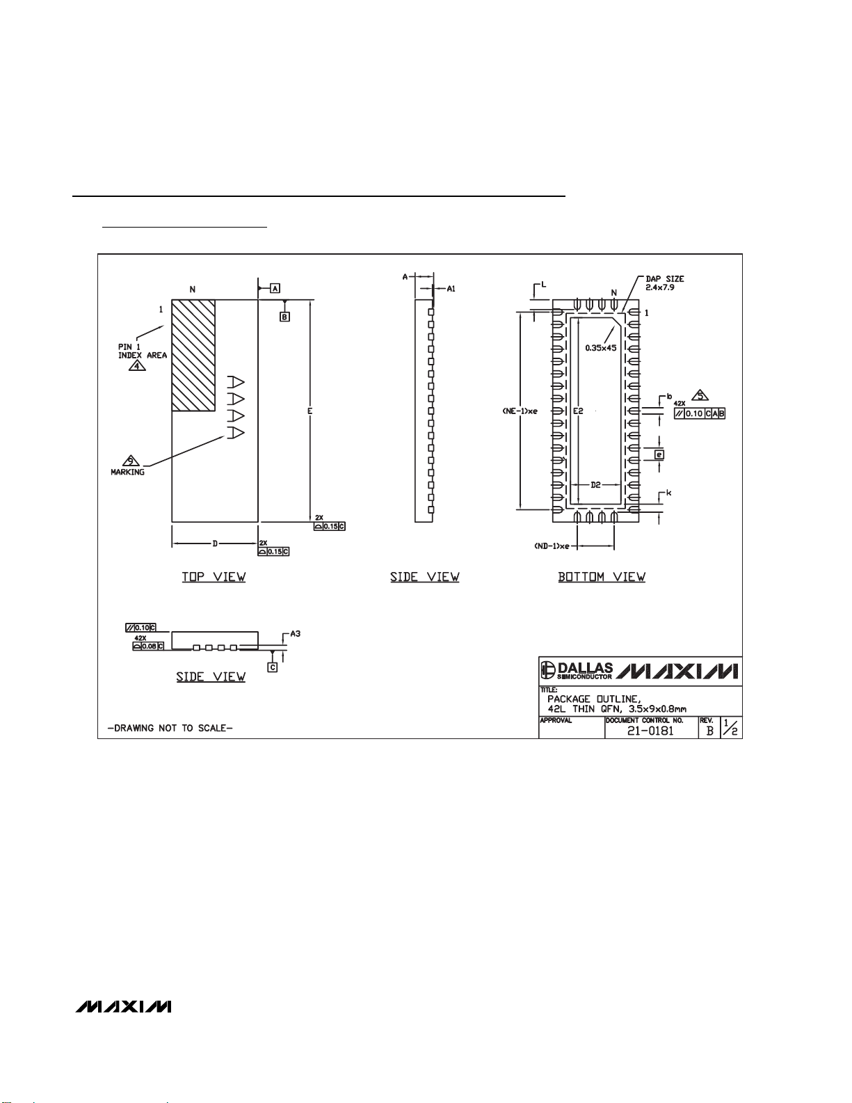
Package Information
(The package drawing(s) in this data sheet may not reflect the most current specifications. For the latest package outline information,
go to www.maxim-ic.com/packages
.)
42L THIN QFN.EPS
°
Page 12

MAX4886
Quad, High-Speed HDMI/DVI 2:1 Digital Video
Switch
Maxim cannot assume responsibility for use of any circuitry other than circuitry entirely embodied in a Maxim product. No circuit patent licenses are
implied. Maxim reserves the right to change the circuitry and specifications without notice at any time.
12 ____________________Maxim Integrated Products, 120 San Gabriel Drive, Sunnyvale, CA 94086 408-737-7600
© 2007 Maxim Integrated Products is a registered trademark of Maxim Integrated Products, Inc.
Boblet
Package Information (continued)
(The package drawing(s) in this data sheet may not reflect the most current specifications. For the latest package outline information,
go to www.maxim-ic.com/packages
.)
 Loading...