

Page 1
现货库存、技术资料、百科信息、热点资讯,精彩尽在鼎好!
General Description
The MAX4864L/MAX4865L/MAX4866L/MAX4867/
MAX4865/MAX4866 overvoltage protection controllers
protect low-voltage systems against high-voltage faults
up to +28V, and negative voltages down to -28V. These
devices drive a low-cost complementary MOSFET. If the
input voltage exceeds the overvoltage threshold, these
devices turn off the n-channel MOSFET to prevent damage to the protected components. If the input voltage
drops below ground, the devices turn off the p-channel
MOSFET to prevent damage to the protected components. An internal charge pump eliminates the need for
external capacitors and drives the MOSFET GATEN for
a simple, robust solution.
The overvoltage thresholds are preset to +7.4V
(MAX4864L), +6.35V (MAX4865L), +5.8V (MAX4866L),
and +4.65V (MAX4867). When the input voltage drops
below the undervoltage lockout (UVLO) threshold, the
devices enter a low-current standby mode (8.5µA). Also in
shutdown (EN set to logic-high), the current is reduced further (0.4µA). The MAX4864L/MAX4865L/MAX4866L have
a +2.85V UVLO threshold, and the MAX4867 has a +2.5V
UVLO threshold. The MAX4865/MAX4866 have a 4.15V
UVLO threshold.
In addition, a ±15kV ESD protection is provided to the
input when bypassed with a 1µF capacitor to ground. All
devices are offered in a small 6-pin SOT23 and a 6-pin,
2mm x 2mm µDFN package, and are specified for
operation over the -40°C to +85°C temperature range.
Applications
Features
♦ Overvoltage Protection Up to +28V
♦ Reverse Polarity Protection Down to -28V
♦ Preset Overvoltage (OV) Trip Level (7.4V, 6.35V,
5.8V, 4.65V)
♦ Drive Low-Cost Complementary MOSFET
♦ Internal 50ms Startup Delay
♦ Internal Charge Pump
♦ 8.5µA Standby Current (In UVLO Mode)
♦ 0.4µA Shutdown Current
♦ Overvoltage Fault FLAG Indicator
♦ 6-Pin (2mm x 2mm) µDFN and 6-Pin SOT23
Packages
MAX4864L/MAX4865L/MAX4866L/MAX4867/MAX4865/MAX
4866
Overvoltage Protection Controllers
with Reverse Polarity Protection
________________________________________________________________ Maxim Integrated Products 1
19-3582; Rev 1; 5/06
For pricing, delivery, and ordering information, please contact Maxim/Dallas Direct! at
1-888-629-4642, or visit Maxim’s website at www.maxim-ic.com.
Ordering Information
PA R T
PIN -
OV T RIP
)
TOP
PKG
CODE
M A X4 8 6 4 L E U T- T
7.40
—
M AX 4864LE LT 6 µD FN 7.40
L622-1
M A X4 8 6 5 L E U T- T
6.35
—
M AX 4865LE LT 6 µD FN 6.35
L622-1
M A X4 8 6 6 L E U T- T
5.80
—
M AX 4866LE LT 6 µD FN 5.80
L622-1
M A X4 8 6 7 E U T- T
4.65
—
M AX 4867E LT 6 µD FN 4.65
L622-1
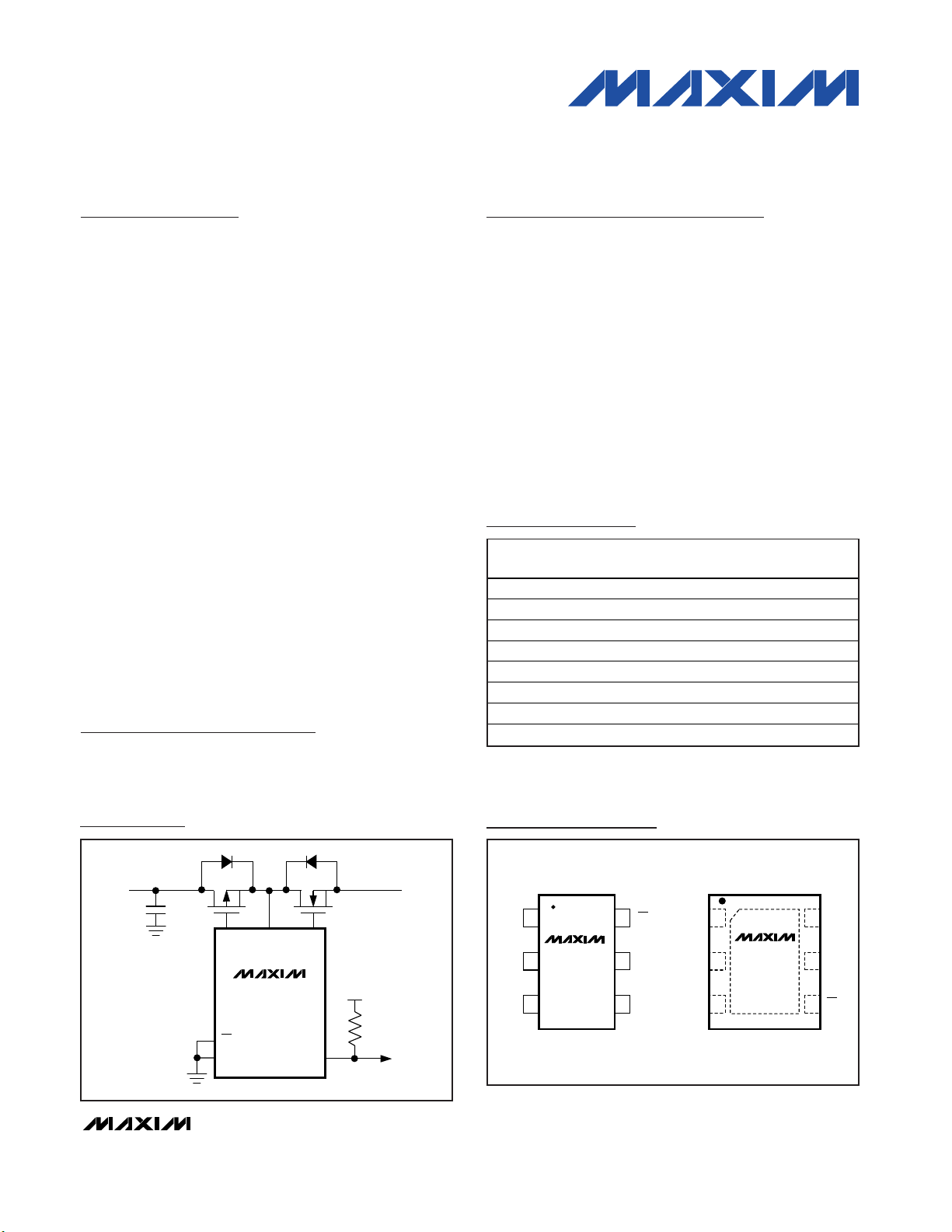
Functional Diagram appears at end of data sheet.
Note: All devices are specified over the -40°C to +85°C operating
range.
ADAPTER
(-28V TO +28V)
OUTPUT
V
IO
IN
FLAG
GATEN
1µF
GND
EN
GATEP
MAX4864L
MAX4865L
MAX4866L
MAX4867
PN
Typical Operating Circuit
Pin Configurations
GND
GATENFLAG
16EN
5 GATEP
IN
MAX4864L
MAX4865L
MAX4866L
MAX4867
SOT23
TOP VIEW
2
34
FLAG
ENIN
GATEN
GATEP
GND
MAX4864L
MAX4865L
MAX4866L
MAX4867
µDFN
1
2
3
6
5
4
Cell Phones
Digital Still Cameras
PDAs and Palmtop Devices
MP3 Players
PA C K A G E
6 S OT23- 6
6 S OT23- 6
6 S OT23- 6
6 S OT23- 6
LEVEL (V
MARK
ABVO
AAE
ABVP
AAF
ABVQ
AAG
ABVN
AAD
Page 2
MAX4864L/MAX4865L/MAX4866L/MAX4867
Overvoltage Protection Controllers
with Reverse Polarity Protection
2 _______________________________________________________________________________________
ABSOLUTE MAXIMUM RATINGS
Stresses beyond those listed under “Absolute Maximum Ratings” may cause permanent damage to the device. These are stress ratings only, and functional
operation of the device at these or any other conditions beyond those indicated in the operational sections of the specifications is not implied. Exposure to
absolute maximum rating conditions for extended periods may affect device reliability.
IN to GND ..............................................................-0.3V to +30V
GATEN, GATEP to GND ........................................-0.3V to +12V
IN to GATEP ...........................................................-0.3V to +20V
FLAG, EN to GND ....................................................-0.3V to +6V
Continuous Power Dissipation (T
A
= +70°C)
6-Pin µDFN (2mm x 2mm) (derate 2.1mW/°C
above +70°C) ..............................................................168mW
6-Pin SOT23 (derate 8.7mW/°C above +70°C)............696mW
Operating Temperature Range ..........................-40°C to +85°C
Junction Temperature .................................................... +150°C
Storage Temperature Range ............................-65°C to +150°C
Lead Temperature (soldering, 10s) ................................+300°C
ELECTRICAL CHARACTERISTICS
(VIN= +5V (MAX4864L/MAX4865L/MAX4866L), VIN= +4V (MAX4867), TA= -40°C to +85°C, C
GATEN
= 500pF, unless otherwise
noted. Typical values are at T
A
= +25°C.) (Note 1)
PARAMETER
SYMBOL
CONDITIONS
MIN
TYP
MAX
UNITS
Input Voltage Range V
IN
V
MAX4864L
MAX4865L
MAX4866L
Overvoltage Trip Level
VIN rising
MAX4867
V
MAX4864L 75
MAX4865L 65
MAX4866L 55
Overvoltage Lockout
Hysteresis
MAX4867 50
mV
MAX4864L/MAX4865L/MAX4866L
Undervoltage Lockout
Threshold
VIN falling
MAX4867
V
MAX4864L/MAX4865L/MAX4866L 44
Undervoltage Lockout
Hysteresis
MAX4867 25
mV
MAX4864L/MAX4865L/MAX4866L 77
IN Supply Current I
IN
MAX4867 68
µA
MAX4864L/MAX4865L/MAX4866L,
V
IN
= +2.6V
22
UVLO Supply Current I
UVLO
MAX4867, V
IN
= +2.2V 8 18
µA
MAX4864L/MAX4865L/MAX4866L,
V
IN
= 3.6V
2
Shutdown Supply Current I
SHD
MAX4867, V
IN
= 3.6V
2
µA
MAX4864L/MAX4865L/MAX4866L 9
10
GATEN Voltage
1µA load
MAX4867
V
GATEN Pulldown Current I
PD
V
IN
> OVLO, V
GATEN
= +5.5V 12 32 65 mA
GATEP Clamp Voltage
V
GATEP Pulldown Resistor
32 48 64 kΩ
FLAG Output-Low Voltage V
OL
I
SINK
= 1mA
V
FLAG Leakage Current V
FLAG
= +5.5V 1 µA
EN Input-High Voltage V
IH
V
EN Input-Low Voltage V
IL
V
OVLO
1.2 28.0
7.0 7.4 7.8
5.95 6.35 6.75
5.45 5.8 6.15
4.35 4.65 4.95
UVLO
V
GATEN
V
CLAMP
R
GATEP
EN = GND
EN = GND
EN = 1.6V
2.65 2.85 3.05
2.3 2.5 2.7
7.5 7.85 8.0
13.5 16.5 19.5
1.5
8.5
0.4
0.4
9.83
120
110
0.4
0.4
Page 3
MAX4864L/MAX4865L/MAX4866L/MAX4867
Overvoltage Protection Controllers
with Reverse Polarity Protection
_______________________________________________________________________________________ 3
ELECTRICAL CHARACTERISTICS (continued)
(VIN= +5V (MAX4864L/MAX4865L/MAX4866L), VIN= +4V (MAX4867), TA= -40°C to +85°C, C
GATEN
= 500pF, unless otherwise
noted. Typical values are at T
A
= +25°C.) (Note 1)
PARAMETER
SYMBOL
CONDITIONS
MIN
TYP
MAX
UNITS
EN Input Leakage Current I
LKG
EN = GND or +5.5V 1 µA
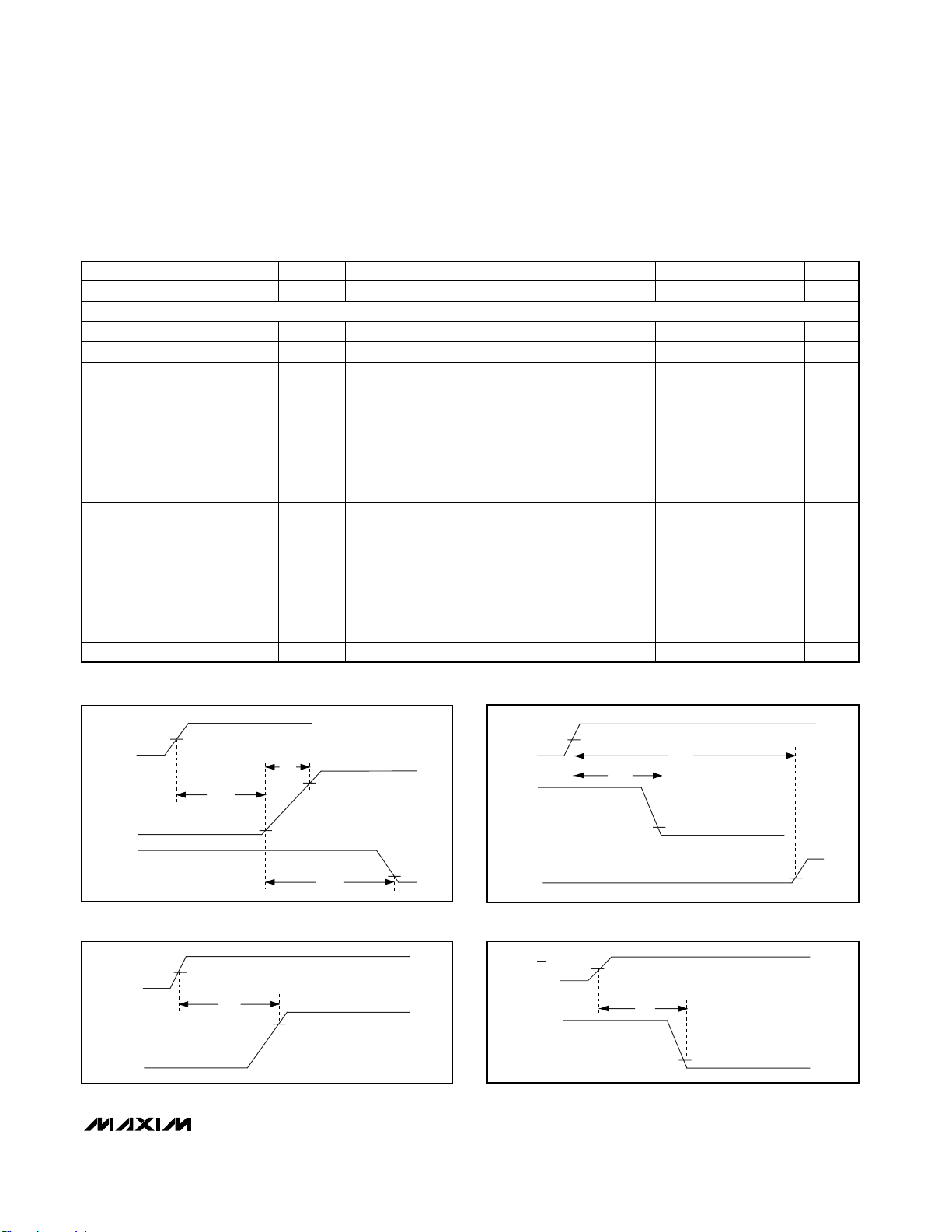
TIMING
Startup Delay
V
IN
> UVLO to V
GATEN
> 0.3V, Figure 1 20 50 80 ms
FLAG Blanking Time
V
GATEN
> 0.3V to V
FLAG
< 0.3V, Figure 1 20 50 80 ms
GATEN Turn-On Time t
GON
C
GATEN
= 500pF, V
GATEN
= 0.3V to +8V
(MAX4864L/MAX4865L/MAX4866L)
V
GATEN
= 0.3V to +7V (MAX4867), Figure 1
10 ms
GATEN Turn-Off Time t
Goff
V
I N
r i si ng at 3V /µs fr om + 5V to + 8V
( M AX 4864L/M AX 4865L/M AX 4866L) ,
or fr om + 4V to + 7V ( M AX 4867)
V
GAT E N
= 0.3V , C
GAT E N
= 500p F, Fi g ur e 2
720µs
FLAG Assertion Delay t
FLAG
VIN rising at 3V/µs from 5V to 8V
( M AX 4864L/M AX 4865L/M AX 4866L) ,
or from +4V to +7V (MAX4867), V
FLAG
= 0.3V,
Figure 2
µs
Initial Overvoltage Fault Delay t
OVP
VIN rising at 3V/µs from 0V to +9V, time from
V
IN
= 5V to I
GATEN
= 80% of I
PD
(GATEN pulldown
current), Figure 3
µs
Disable Time t
DIS
VEN = +2.4V, V
GATEN
= 0.3V, Figure 4 2 µs
Note 1: All parts are 100% tested at +25°C. Electrical limits across the full temperature range are guaranteed by design and correlation.
V
GATEN
V
EN
+0.3V
+2.4V
t
DIS
Figure 4. Disable Timing Diagram
V
IN
V
UVLO
t
GON
t
START
V
GATEN
V
FLAG
t
BLANK
+0.3V
+8V (+7V)*
*MAX4867
+5V
+0.3V
Figure 1. Startup Timing Diagram
V
IN
V
OVLO
V
GATEN
V
FLAG
t
FLAG
t
GOFF
+0.3V
+0.3V
+5V
Figure 2. Shutdown Timing Diagram
V
IN
V
OVLO
t
OVP
I
GATEN
80%
0V
Figure 3. Power-Up Overvoltage Timing Diagram
t
START
t
BLANK
3.5
1.5
Page 4
MAX4864L/MAX4865L/MAX4866L/MAX4867
Overvoltage Protection Controllers
with Reverse Polarity Protection
4 _______________________________________________________________________________________
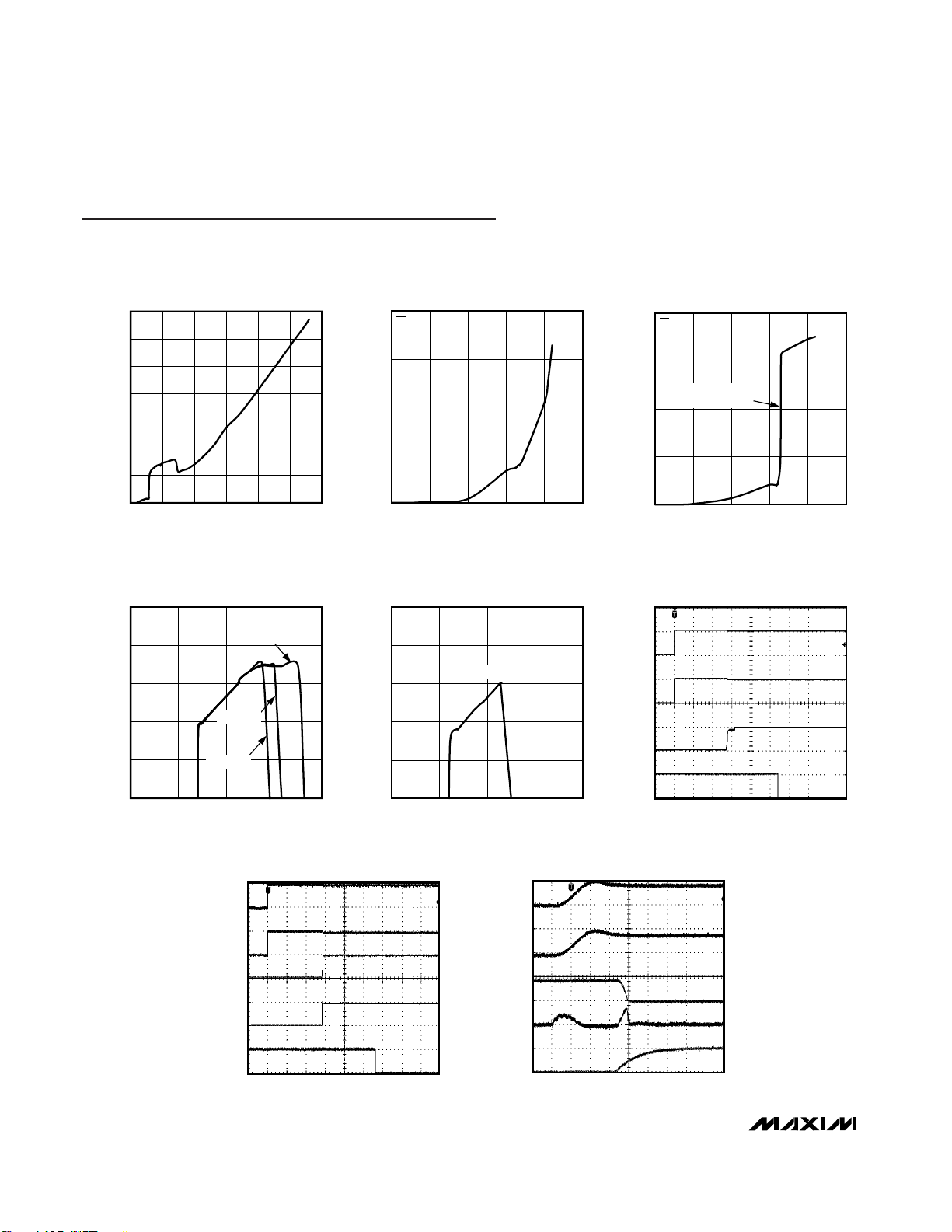
Typical Operating Characteristics
(TA = +25°C, unless otherwise noted.)
Typical Operating Characteristics
(TA = +25°C, unless otherwise noted.)
SUPPLY CURRENT vs. SUPPLY VOLTAGE
(MAX4864L)
MAX4864 toc01
SUPPLY VOLTAGE (V)
SUPPLY CURRENT (µA)
252015105
50
100
150
200
250
300
350
0
030
REVERSE CURRENT vs. OUTPUT VOLTAGE
(MAX4864L)
MAX4864 toc02
OUTPUT VOLTAGE (V)
REVERSE CURRENT (µA)
4321
0.1
0.2
0.3
0.4
0
05
EN = 3V
REVERSE CURRENT vs. OUTPUT VOLTAGE
(MAX4864L)
MAX4864 toc03
OUTPUT VOLTAGE (V)
REVERSE CURRENT (µA)
4321
20
40
60
80
0
05
EN = 0V
DEVICE TURNS ON
AT TRANSITION
MAX4864L/MAX4865L/MAX4866L
GATEN VOLTAGE vs. INPUT VOLTAGE
MAX4864 toc04
INPUT VOLTAGE (V)
GATEN VOLTAGE (V)
642
3
6
9
12
15
0
08
MAX4864L
MAX4865L
MAX4866L
MAX4867
GATEN VOLTAGE vs. INPUT VOLTAGE
MAX4864 toc05
INPUT VOLTAGE (V)
GATEN VOLTAGE (V)
642
3
6
9
12
15
0
08
MAX4867
POWER-UP RESPONSE
MAX4864 toc06
20ms/div
10V
0V
5V
0V
IN
GATEN
FLAG
5V
0V
ADAPTER
5V
0V
POWER-UP RESPONSE
MAX4864 toc07
IN
5V/div
FLAG
5V/div
OUT
5V/div
ADAPTER
5V/div
20ms/div
IIN
1A/div
OVERVOLTAGE RESPONSE
MAX4864 toc08
IN
FLAG
5V/div
GATEN
5V/div
ADAPTER
2µs/div
I
GATEN
10mA/div
5V
8V
5V
8V
Page 5

MAX4864L/MAX4865L/MAX4866L/MAX4867
Overvoltage Protection Controllers
with Reverse Polarity Protection
_______________________________________________________________________________________ 5
POWER-UP OVERVOLTAGE RESPONSE
MAX4864 toc09
IN
FLAG
GATEN
ADAPTER
20ms/div
8V
0V
8V
0V
5V
0V
0V
NEGATIVE VOLTAGE RESPONSE
MAX4864 toc10
GATEP
FLAG
IN
ADAPTER
20ms/div
0V
0V
5V
0V
5V
0V
PIN
MAX4864LEUT/
MAX4865LEUT/
MAX4866LEUT/
MAX4867EUT
MAX4865LELT/
MAX4867ELT
NAME
FUNCTION
13IN Voltage Input. IN is both the power-supply input and the overvoltage sense input.
21
Ground
32
Faul t- Ind i cati on Outp ut. When E N g oes hi g h, FLAG b ecom es hi g h- i m p ed ance. FLAG
i s asser ted hi g h d ur i ng und er vol tag e l ockout and over vol tag e l ockout cond i ti ons.
FLAG i s d easser ted d ur i ng nor m al op er ati on. FLAG i s an op en- d r ai n outp ut.
46
n-Channel MOSFET Gate-Drive Output. GATEN is the output of an on-chip charge
pump. When V
UVLO
< VIN < V
OVLO
, GATEN is driven high to turn on the external
n-channel MOSFET.
55
p-Channel MOSFET Gate-Drive Output. GATEP is always on when input is above
ground and off when input drops below ground.
64EN
Active-Low Enable Input. Connect to ground in normal operation. Drive EN high to
disable device and enter shutdown mode.
Pin Description
Typical Operating Characteristics (continued)
(TA= +25°C, unless otherwise noted.)
MAX4864LELT/
MAX4866LELT/
GND
FLAG
GATEN
GATEP
Page 6

MAX4864L/MAX4865L/MAX4866L/MAX4867
Overvoltage Protection Controllers
with Reverse Polarity Protection
6 _______________________________________________________________________________________
Detailed Description
The MAX4864L/MAX4865L/MAX4866L/MAX4867 provide
up to +28V overvoltage and negative voltage protection
for low voltage systems. When the input voltage exceeds
the overvoltage trip level, the MAX4864L/MAX4865L/
MAX4866L/MAX4867 turn off a low-cost external n-channel
MOSFET to prevent damage to the protected components. The devices also drive an external p-channel
MOSFET to protect against negative voltage inputs. An
internal charge-pump (see the Functional Diagram),
drives the MOSFET GATEN for a simple, robust solution.
On power-up, the device waits for 50ms before driving
GATEN high. The open-drain FLAG output is kept at a
high impedance for an additional 50ms after GATEN goes
high before deasserting. The FLAG output asserts high
immediately to an overvoltage fault.
Undervoltage Lockout (UVLO)
The MAX4864L/MAX4865L/MAX4866L/MAX4867 have
a fixed +2.85V typical UVLO level, and the MAX4867
has +2.5V UVLO level. When VINis less than the UVLO,
the GATEN driver is held low and FLAG is asserted.
Overvoltage Lockout (OVLO)
The MAX4864L has a +7.4V typical OVLO threshold;
the MAX4865L has +6.35V typical OVLO threshold; the
MAX4866L has a +5.8V typical OVLO threshold; and
the MAX4867 has a +4.65V typical OVLO threshold.
When VINis greater than OVLO, the GATEN driver is
held low and FLAG is asserted.
FLAG Output
The open-drain FLAG output is used to signal to the
host system when there is a fault with the input voltage.
On power-up, FLAG is held high for 50ms after GATEN
turns on, before deasserting. FLAG asserts immediately
to overvoltage and undervoltage faults. When the fault
condition is removed, FLAG deasserts 50ms after
GATEN turns on. Connect a pullup resistor from FLAG
to the logic I/O voltage of the host system.
GATEN Driver
An on-chip charge pump is used to drive GATEN
above IN, allowing the use of a low-cost n-channel
MOSFET. The charge pump operates from the internal
+5.5V regulator.
The actual GATEN output voltage tracks approximately
two times V
IN
until VINexceeds +5.5V, or the OVLO trip
level is exceeded, whichever comes first. The
MAX4864L has a +7.4V typical OVLO, therefore GATEN
remains relatively constant at approximately +10.5V for
+5.5V < VIN< +7.4V. The MAX4866L has a +5.8V typical OVLO, but this can be as low as +5.5V. The GATEN
output voltage is a function of input voltage, as shown
in the Typical Operating Characteristics.
GATEP Driver
When the input voltage drops below ground, GATEP
goes high turning the external p-channel MOSFET off.
When the input voltage goes above ground, GATEP
pulls low and turns on the p-channel MOSFET. An internal clamp protects the p-channel MOSFET by insuring
that the GATEP-to-IN voltage does not exceed +16V
when the input (IN) rises to +28V.
Device Operation
The MAX4864L/MAX4865L/MAX4866L/MAX4867 have
an on-board state machine to control device operation.
A flowchart is shown in Figure 5. On initial power-up, if
VIN< UVLO or if VIN> OVLO, GATEN is held at 0V and
FLAG is high.
If UVLO < VIN< OVLO, the device enters startup after a
50ms internal delay. The internal charge pump is
enabled, and GATEN begins to be driven above VINby
the internal charge pump. FLAG is held high during
startup until the FLAG blanking period expires, typically
50ms after the GATEN starts going high. At this point,
the device is in its on-state.
At any time if VINdrops below UVLO, FLAG is driven
high and GATEN is driven to ground.
STANDBY
GATEN = 0
FLAG = HIGH
TIMER STARTS
COUNTING
V
IN
> UVLO
V
IN
< UVLO
V
IN
> OVLO
V
IN
> OVLO
OVLO CHECK
GATEN = 0
FLAG = HIGH
STARTUP
GATEN DRIVEN HIGH
FLAG = HIGH
ON
GATEN HIGH
FLAG = LOW
t = 50ms
t = 50ms
Figure 5. State Diagram
Page 7

MAX4864L/MAX4865L/MAX4866L/MAX4867
Overvoltage Protection Controllers
with Reverse Polarity Protection
_______________________________________________________________________________________ 7
Applications Information
MOSFET Configuration
The MAX4864L/MAX4865L/MAX4866L/MAX4867 can be
used with either a complementary MOSFET configuration
as shown in the Typical Operating Circuit, or can be configured with a single p-channel MOSFET and back-toback n-channel MOSFETs as shown in Figure 6.
The MAX4864L/MAX4865L/MAX4866L/MAX4867 can drive
either a complementary MOSFET or a single p-channel
MOSFET and back-to-back n-channel MOSFETs. The
back-to-back configuration has almost zero reverse current when the adapter is not present or when the
adapter voltage is below the UVLO threshold.
If reverse current leakage is not a concern, a single
MOSFET can be used. This approach has half the loss
of the back-to-back configuration when used with similar MOSFET types and is a lower cost solution. Note
that if the input is actually pulled low, the output will
also be pulled low due to the parasitic body diode in
the MOSFET. If this is a concern, then the back-to-back
configuration should be used.
MOSFET Selection
The MAX4864L/MAX4865L/MAX4866L/MAX4867 are
designed for use with a complementary MOSFET or single p-channel and dual back-to-back n-channel
MOSFETs. In most situations, MOSFETs with RDS(ON)
specified for a VGS of 4.5V work well. Also the V
DS
should be +30V for the MOSFET to withstand the full
+28V IN range of the MAX4864L/MAX4865L/
MAX4866L/MAX4867. Table 1 shows a selection of
MOSFETs which are appropriate for use with the
MAX4864L/MAX4865L/MAX4866L/MAX4867.
IN Bypass Considerations
For most applications, bypass ADAPTER to GND with a
1µF ceramic capacitor. If the power source has significant inductance due to long lead length, take care to
prevent overshoots due to the LC tank circuit and provide protection if necessary to prevent exceeding the
+30V absolute maximum rating on IN.
ESD Test Conditions
ESD performance depends on a number of conditions. The
MAX4864L/MAX4865L/MAX4866L/MAX4867 are specified
for +/-15kV typical ESD resistance on IN when ADAPTER is
bypassed to ground with a 1µF ceramic capacitor.
Human Body Model
Figure 7 shows the Human Body Model, and Figure 8
shows the current waveform it generates when discharged into a low impedance. This model consists of a
100pF capacitor charged to the ESD voltage of interest,
which is then discharged into the device through a
1.5kΩ resistor.
P
NN
ADAPTER
-28V TO +28V
OUTPUT
V
IO
IN
FLAG
GATEN
1µF
GND
GATEP
MAX4864L
MAX4865L
MAX4866L
MAX4867
Figure 6. Back-to-Back External MOSFET Configuration
Table 1. MOSFET Suggestions
PART
CONFIGURATION/
PACKAGE
V
GS
MAX
(V)
VDS MAX
(V)
RON AT 4.5V (mΩ)
MANUFACTURER
+30
Si5504DC
Complementary
MOSFET/1206-8
±20
-30
Si5902DC Dual/1206-8 ±20 +30
Si1426DH Single/µDFN-6 ±20 +30
Si5435DC Single/1206-8 ±20 -30 80 (p-MOSFET)
Vishay Siliconix
FDC6561AN Dual/SSOT-6 ±20 +30
FDG315N Single/µDFN-6 ±20 +30
FDC658P Single/SSOT-6 ±20 -30 75 (p-MOSFET)
FDC654P Single/SSOT-6 ±20 -30
Fairchild Semiconductor
143 (n-MOSFET)
290 (p-MOSFET)
143 (n-MOSFET)
115 (n-MOSFET)
145 (n-MOSFET)
160 (n-MOSFET)
125 (p-MOSFET)
Page 8

MAX4864L/MAX4865L/MAX4866L/MAX4867
Overvoltage Protection Controllers
with Reverse Polarity Protection
8 _______________________________________________________________________________________
IEC 1000-4-2
Since January 1996, all equipment manufactured
and/or sold in the European Union has been required to
meet the stringent IEC 1000-4-2 specification. The IEC
1000-4-2 standard covers ESD testing and performance of finished equipment. It does not specifically
refer to ICs. The MAX4864L/MAX4865L/MAX4866L/
MAX4867 help users design equipment that meets
Level 3 of IEC 1000-4-2, without additional ESD-protection components.
The main difference between tests done using the
Human Body Model and IEC 1000-4-2 is higher peak
current in IEC 1000-4-2. Because series resistance is
lower in the IEC 1000-4-2 ESD test model (Figure 9), the
ESD-withstand voltage measured to this standard is gen-
erally lower than that measured using the Human Body
Model. Figure 10 shows the current waveform for the
±8kV IEC 1000-4-2 Level 4 ESD Contact Discharge test.
The Air-Gap test involves approaching the device with a
charger probe. The Contact Discharge method connects
the probe to the device before the probe is energized.
Chip Information
TRANSISTOR COUNT: 727
PROCESS TECHNOLOGY: BiCMOS
CHARGE-CURRENT
LIMIT RESISTOR
DISCHARGE
RESISTANCE
STORAGE
CAPACITOR
C
s
100pF
R
C
1MΩ
R
D
1.5Ω
HIGH-
VOLTAGE
DC
SOURCE
DEVICE
UNDER
TEST
Figure 7. Human Body ESD Test Model
IP 100%
90%
36.8%
t
RI
TIME
t
DL
CURRENT WAVEFORM
PEAK-TO-PEAK RINGING
(NOT DRAWN TO SCALE)
I
r
10%
0
0
AMPERES
Figure 8. Human Body Current Waveform
tR = 0.7ns TO 1ns
30ns
60ns
t
100%
90%
10%
I
PEAK
I
Figure 10. IEC 1000-4-2 ESD Generator Current Waveform
CHARGE-CURRENT
LIMIT RESISTOR
DISCHARGE
RESISTANCE
STORAGE
CAPACITOR
C
s
150pF
R
C
50Ω TO 100Ω
R
D
330Ω
HIGH-
VOLTAGE
DC
SOURCE
DEVICE
UNDER
TEST
Figure 9. IEC 1000-4-2 ESD Test Model
Page 9

MAX4864L/MAX4865L/MAX4866L/MAX4867
Overvoltage Protection Controllers
with Reverse Polarity Protection
_______________________________________________________________________________________ 9
PN
ADAPTER
OUTPUT
V
IO
IN
FLAG
GATEN
GND
EN
GATEP
MAX4864L
MAX4865L
MAX4866L
MAX4867
+15V CLAMP
+5.5V
REGULATOR
UVLO AND OVLO
DETECTOR
2x CHARGE
PUMP
CONTROL
LOGIC AND TIMER
GATE
DRIVER
Functional Diagram
Page 10

MAX4864L/MAX4865L/MAX4866L/MAX4867
Overvoltage Protection Controllers
with Reverse Polarity Protection
10 ______________________________________________________________________________________
6, 8, 10L UDFN.EPS
EVEN TERMINAL
L
C
ODD TERMINAL
L
C
L
e
L
A
e
E
D
PIN 1
INDEX AREA
b
e
A
b
N
SOLDER
MASK
COVERAGE
A A
1
PIN 1
0.10x45∞
L
L1
(N/2 -1) x e)
XXXX
XXXX
XXXX
SAMPLE
MARKING
A1
A2
7
A
1
2
21-0164
PACKAGE OUTLINE,
6, 8, 10L uDFN, 2x2x0.80 mm
-DRAWING NOT TO SCALE-
Package Information
(The package drawing(s) in this data sheet may not reflect the most current specifications. For the latest package outline information,
go to www.maxim-ic.com/packages
.)
Page 11

MAX4864L/MAX4865L/MAX4866L/MAX4867
Overvoltage Protection Controllers
with Reverse Polarity Protection
______________________________________________________________________________________ 11
COMMON DIMENSIONS
SYMBOL MIN. NOM.
A
0.70 0.75
A1
D 1.95 2.00
E
1.95 2.00
L
0.30 0.40
PKG. CODE N e b
PACKAGE VARIATIONS
L1
6L622-1 0.65 BSC 0.30±0.05
0.25±0.050.50 BSC8L822-1
0.20±0.030.40 BSC10L1022-1
2.05
0.80
MAX.
0.50
2.05
0.10 REF.
(N/2 -1) x e
1.60 REF.
1.50 REF.
1.30 REF.
A2
-
-DRAWING NOT TO SCALE-
A
2
2
21-0164
PACKAGE OUTLINE,
6, 8, 10L uDFN, 2x2x0.80 mm
0.15 0.20 0.25
0.020 0.025 0.035
Package Information (continued)
(The package drawing(s) in this data sheet may not reflect the most current specifications. For the latest package outline information,
go to www.maxim-ic.com/packages
.)
Page 12

MAX4864L/MAX4865L/MAX4866L/MAX4867
Overvoltage Protection Controllers
with Reverse Polarity Protection
Maxim cannot assume responsibility for use of any circuitry other than circuitry entirely embodied in a Maxim product. No circuit patent licenses are
implied. Maxim reserves the right to change the circuitry and specifications without notice at any time.
12 ____________________Maxim Integrated Products, 120 San Gabriel Drive, Sunnyvale, CA 94086 408-737-7600
© 2006 Maxim Integrated Products is a registered trademark of Maxim Integrated Products, Inc.
6LSOT.EPS
PACKAGE OUTLINE, SOT 6L BODY
21-0058
1
1
G
Package Information (continued)
(The package drawing(s) in this data sheet may not reflect the most current specifications. For the latest package outline information,
go to www.maxim-ic.com/packages
.)
 Loading...