

Page 1
General Description
The MAX4820/MAX4821 8-channel relay drivers offer
built-in kickback protection and drive +3.3V/+5V nonlatching or dual-coil-latching relays. These devices are
especially useful when driving +3V relays. Each independent open-drain output features a 2Ω on-resistance
and is guaranteed to sink 70mA (min) of load current.
Both devices consume less than 50µA (max) quiescent
current and have 1µA output off-leakage current.
The MAX4820 features an SPI™-/QSPI™-/MICROWIRE™compatible serial interface. Input data is shifted into an 8bit shift register and latched to the outputs when CS
transitions from low to high. Each data bit in the shift register corresponds to a specific output, allowing independent control of all outputs.
The MAX4821 features a 4-bit (A0, A1, A2, LVL) parallel-input interface. The first three bits (A0, A1, A2) determine the output address, and the fourth bit (LVL)
determines whether the selected output is switched on
or off. Data is latched to the outputs when CS transitions from low to high.
Both devices feature separate set and reset functions
that allow the user to turn on or turn off all outputs simultaneously with a single control line. Built-in hysteresis
(Schmidt trigger) on all digital inputs allows this device
to be used with slow rising and falling signals, such as
those from optocouplers or RC power-up initialization
circuits. The MAX4820/MAX4821 are available in 20-pin
TSSOP and space-saving 20-pin thin QFN packages.
Applications
Central Office
ATE
DSL, ADSL Line Cards
Industrial Equipment
E1/T1 Redundancy
Features
♦ 8 Independent Output Channels
♦ Built-In Inductive Kickback Protection
♦ Drive +3V and +5V Relays
♦ Guaranteed 70mA (min) Coil Drive Current
♦ SET Function to Turn On All Outputs
Simultaneously
♦ RESET Function to Turn Off All Outputs
Simultaneously
♦ SPI-/QSPI-/MICROWIRE-Compatible Serial
Interface (MAX4820)
♦ Serial Digital Output for Daisy Chaining
(MAX4820)
♦ Parallel Interface (MAX4821)
♦ Low 50µA (max) Quiescent Supply Current
♦ Space-Saving 20-Pin Thin QFN Package
MAX4820/MAX4821
+3.3V/+5V, 8-Channel, Cascadable Relay Drivers
with Serial/Parallel Interface
________________________________________________________________ Maxim Integrated Products 1
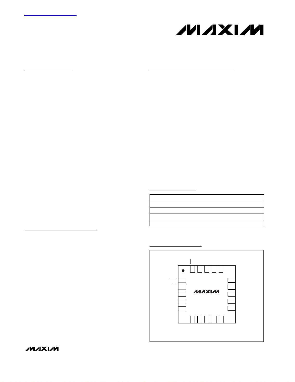
Pin Configurations
Ordering Information
19-2751; Rev 0; 1/03
For pricing, delivery, and ordering information, please contact Maxim/Dallas Direct! at
1-888-629-4642, or visit Maxim’s website at www.maxim-ic.com.
*For maximum heat dissipation, packages have an exposed pad
(EP) on the bottom. Solder exposed pad to GND.
Pin Configurations continued at end of data sheet.
Typical Application Circuits and Functional Diagrams
appear at end of data sheet.
SPI and QSPI are trademarks of Motorola, Inc.
MICROWIRE is a trademark of National Semiconductor Corp.
查询MAX4820供应商
PART TEMP RANGE PIN-PACKAGE
MAX4820ETP* -40°C to +85°C 20 Thin QFN-EP
MAX4820EUP* -40°C to +85°C 20 TSSOP
MAX4821ETP* -40°C to +85°C 20 Thin QFN-EP
MAX4821EUP* -40°C to +85°C 20 TSSOP
TOP VIEW
SET
VCCOUT1
OUT2
20
19
18
17
16 PGND
1
RESET
DIN
SCLK
2
CS
3
4
5DOUT
MAX4820
6
7
N.C.
GND
THIN QFN
8
OUT8
9
OUT7
10PGND
OUT3
15
OUT4
14
COM
13
12
OUT5
11
OUT6
Page 2
MAX4820/MAX4821
+3.3V/+5V, 8-Channel, Cascadable Relay Drivers
with Serial/Parallel Interface
2 _______________________________________________________________________________________
ABSOLUTE MAXIMUM RATINGS
ELECTRICAL CHARACTERISTICS
(VCC= +3V to +5.5V, V
COM
= VCC, TA= -40°C to +85°C, unless otherwise noted. Typical values are at TA= +25°C.) (Note 1)
Stresses beyond those listed under “Absolute Maximum Ratings” may cause permanent damage to the device. These are stress ratings only, and functional
operation of the device at these or any other conditions beyond those indicated in the operational sections of the specifications is not implied. Exposure to
absolute maximum rating conditions for extended periods may affect device reliability.
(All voltages referenced to GND.)
V
CC
, COM..............................................................-0.3V to +6.0V
OUT_........................................................-0.3V to (V
COM
+ 0.3V)
CS, SCLK, DIN, SET, RESET, A0, A1, A2, LVL......-0.3V to +6.0V
DOUT..........................................................-0.3V to (V
CC
+ 0.3V)
Continuous OUT_ Current (all outputs turned on) ............150mA
Continuous OUT_ Current (single output turned on) ........300mA
Continuous Power Dissipation (T
A
= +70°C)
20-Lead Thin QFN
(derate 16.9mW/°C above +70°C).................................1350mW
θ
JA
.........................................................................59.3°C/W
20-Pin TSSOP
(derate 21.7mW/°C above +70°C).................................1739mW
θ
JA
............................................................................46°C/W
Operating Temperature Range ...........................-40°C to +85°C
Junction Temperature......................................................+150°C
Storage Temperature Range .............................-65°C to +150°C
Soldering Temperature (10s) ...........................................+300°C
Operating Voltage V
Quiescent Current I
Thermal Shutdown 160 °C
Power-On Reset 0.8 1.5 2.2 V
Power-On Reset Hysteresis 140 mV
DIGITAL INPUTS (SCLK, DIN, CS, LVL, A0, A1, A2, RESET, SET)
Input Logic High Voltage V
Input Logic Low Voltage V
Input Logic Hysteresis V
Input Leakage Currents I
CIN Input Capacitance C
DIGITAL OUTPUT (DOUT)
DOUT Low Voltage V
DOUT High Voltage V
RELAY OUTPUT DRIVERS (OUT1–OUT8)
OUT_ Drive Current
OUT_ On-Resistance R
OUT_ Voltage V
I
OUT
PARAMETER SYMBOL CONDITIONS MIN TYP MAX UNITS
Off-Leakage Current I
CC
I
Q
IH
IL
HYST
LEAK
IN
OL
OH
ON
OUT
LEAK
OUT
logic inputs = 0 or V
VCC = 3.3V 2.0
VCC = 5V 2.4
VCC = 3.3V 0.6
VCC = 5V 0.8
Input voltages = 0 or 5.5V -1.0 0.01 +1.0 µA
I
SINK
I
SOURCE
VCC = 2.7V 70
V
CC
VCC = 2.7V 2 6 Ω
_VCC = 3.0V, I
V
OUT
_ = 0,
= 6mA 0.4 V
= 0.5mA VCC - 0.5 V
= 4.5V 70
_ = 70mA 0.4 V
OUT
_ = VCC, all outputs off -1 +1 µA
VCC = 3.6V 15 50
CC V
= 5.5V 20 70
CC
2.3 5.5 V
150 mV
5pF
µA
V
V
mA
Kickback Diode Forward Voltage V
FORWIOUT
_ = 150mA (Note 2) 1.5 V
Page 3
MAX4820/MAX4821
3.3V/+5V, 8-Channel, Cascadable Relay Drivers
with Serial/Parallel Interface
_______________________________________________________________________________________ 3
ELECTRICAL CHARACTERISTICS (continued)
(VCC= +3V to +5.5V, V
COM
= VCC, TA= -40°C to +85°C, unless otherwise noted. Typical values are at TA= +25°C.) (Note 1)
Note 1: Specifications at -40°C are guaranteed by design and not production tested.
Note 2: After relay turn-off, inductive kickback may momentarily cause the voltage at OUT_ to exceed V
COM
. This is considered part
of normal operation and will not damage the device.
PARAMETER SYMBOL CONDITIONS MIN TYP MAX UNITS
SPI TIMING (MAX4821)
Turn-On Time (OUT_) t
Turn-Off Time (OUT_) t
SCLK Frequency f
Cycle Time t
CS Fall to SCLK Rise Setup t
CS Rise to SCLK Hold t
SCLK High Time t
SCLK Low Time t
Data Setup Time t
Data Hold Time t
SCLK Fall to DOUT Valid t
Rise Time (DIN, SCLK, CS, SET,
RESET)
Fall Time (DIN, SCLK, CS,
RESET, SET)
RESET Min Pulse Width t
SET Min Pulse Width t
PARALLEL TIMING (MAX4820)
Turn-On Time t
Turn-Off Time t
LVL Setup Time t
LVL Hold Time t
Address to CS Setup Time t
Address to CS Hold Time t
Rise Time (A2, A1, A0, LVL) t
Fall Time (A2, A1, A0, LVL) t
RESET Pulse Width t
SET Pulse Width t
From rising edge of CS, RL = 50Ω,
C
= 50pF
L
From rising edge of CS, RL = 50Ω,
C
= 50pF
L
CL
50% of SCLK to 10% of DOUT,
= 50pF
C
L
20% of VCC to 70% of VCC, CL = 50pF 2 µs
20% of VCC to 70% of VCC, CL = 50pF 2 µs
From rising edge of CS, RL = 50Ω,
C
= 50pF
L
From rising edge of CS, RL = 50Ω,
= 50pF
C
L
20% of VCC to 70% of VCC, CL = 50pF 2 µs
20% of VCC to 70% of VCC, CL = 50pF 2 µs
CH
ON
OFF
SCLK
+ t
CSS
CSH
CH
CL
DS
DH
DO
t
SCR
t
SCF
RW
SW
ON
OFF
LS
LH
AH
AS
SCR
SCF
RW
SW
1.0 µs
1.0 µs
0 2.1 MHz
480 ns
240 ns
240 ns
190 ns
190 ns
100 ns
0ns
85 120 ns
70 ns
70 ns
1µs
1µs
100 ns
0ns
100 ns
0ns
70 ns
70 ns
Page 4
MAX4820/MAX4821
+3.3V/+5V, 8-Channel, Cascadable Relay Drivers
with Serial/Parallel Interface
4 _______________________________________________________________________________________
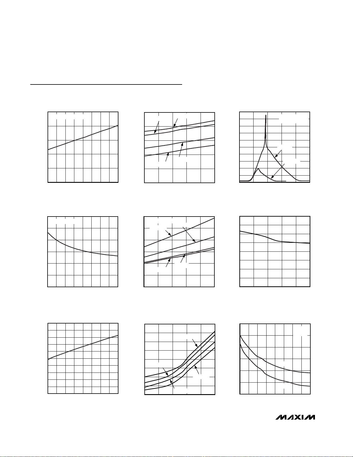
Typical Operating Characteristics
(V
COM
= VCC, TA= -40°C to +85°C, unless otherwise noted. Typical values are at TA= +25°C.)
SUPPLY CURRENT
vs. SUPPLY VOLTAGE
MAX4820 toc01
SUPPLY VOLTAGE (V)
SUPPLY CURRENT (µA)
5.14.74.33.93.53.12.7
5
10
15
20
25
0
2.3 5.5
ALL LOGIC INPUTS = 0
SUPPLY CURRENT
vs. TEMPERATURE
MAX4820 toc02
TEMPERATURE (°C)
SUPPLY CURRENT (µA)
603510-15
5
10
15
20
25
0
-40 85
VCC = 5V
VCC = 5.5V
VCC = 2.3V
VCC = 3.3V
SUPPLY CURRENT
vs. INPUT LOGIC VOLTAGE
MAX4820 toc03
INPUT LOGIC VOLTAGE (V)
SUPPLY CURRENT (µA)
4321
100
200
300
400
500
600
700
800
900
1000
0
05
VCC = 3.3V
VCC = 5V
ALL LOGIC INPUTS
CONNECTED
ON-RESISTANCE
vs. SUPPLY VOLTAGE
MAX4820 toc04
SUPPLY VOLTAGE (V)
R
ON
(Ω)
5.14.74.33.93.53.12.7
0.5
1.0
1.5
2.0
2.5
3.0
0
2.3 5.5
I
OUT_SINK
= 70mA
ON-RESISTANCE
vs. TEMPERATURE
MAX4820 toc05
TEMPERATURE (°C)
R
ON
(Ω)
603510-15
0.5
1.0
1.5
2.0
2.5
3.0
0
-40 85
V
CC
= 3.3V
V
CC
= 2.3V
V
CC
= 5.5V
V
CC
= 5V
I
OUT_SINK
= 70mA
POWER-ON RESET VOLTAGE
vs. TEMPERATURE
MAX4820 toc06
TEMPERATURE (°C)
POWER-ON RESET VOLTAGE (V)
6035-15 10
0.25
0.50
0.75
1.00
1.25
1.50
1.75
2.00
0
-40 85
OUTPUT OFF-LEAKAGE CURRENT
vs. SUPPLY VOLTAGE
MAX4820 toc07
SUPPLY VOLTAGE (V)
OUTPUT OFF-LEAKAGE (nA)
5.14.73.9 4.33.1 3.52.7
0.1
0.2
0.3
0.4
0.5
0.6
0.7
0.8
0.9
1.0
0
2.3 5.5
OUTPUT OFF-LEAKAGE CURRENT
vs. TEMPERATURE
MAX4820 toc08
TEMPERATURE (°C)
OUTPUT OFF-LEAKAGE (nA)
6035-15 10
0.25
0.50
0.75
1.00
1.25
1.50
1.75
2.00
0
-40 85
VCC = 5.5V
VCC = 5V
VCC = 2.3V
VCC = 3.3V
OUT_ TURN-ON/TURN-OFF DELAY TIMES
vs. SUPPLY VOLTAGE
MAX4820 toc09
SUPPLY VOLTAGE (V)
t
ON
/t
OFF
DELAY TIME (ns)
5.14.74.33.93.53.12.7
30
40
50
60
70
80
20
2.3 5.5
RL = 50Ω
C
L
= 50pF
t
ON
t
OFF
Page 5

MAX4820/MAX4821
3.3V/+5V, 8-Channel, Cascadable Relay Drivers
with Serial/Parallel Interface
_______________________________________________________________________________________ 5
Typical Operating Characteristics (continued)
(V
COM
= VCC, TA= -40°C to +85°C, unless otherwise noted. Typical values are at TA= +25°C.)
BACK EMF CLAMPING
WITH STANDARD 3V RELAY
MAX4820 toc11
200µs/div
V
CS
5V/div
0
0
OUT_
1V/div
OUT_ TURNS OFF
VCC = 3.3V
Pin Description
2.50
2.25
2.00
1.75
1.50
1.25
1.00
INPUT LOGIC THRESHOLD (V)
0.75
0.50
MAX4820 MAX4821
THIN
QFN
TSSOP
1313RESET
INPUT LOGIC THRESHOLD
vs. SUPPLY VOLTAGE
2.3 5.5
SUPPLY VOLTAGE (V)
5.14.72.7 3.1 3.5 3.9 4.3
PIN
NAME FUNCTION
THIN
QFN
TSSOP
MAX4820 toc10
Reset Input. Drive RESET low to clear all latches and registers (all outputs
are turned off). RESET overrides all other inputs. If RESET and SET are pulled
low at the same time, then RESET takes precedence.
Chip-Select Input.
MAX4820: Drive CS low to select the device. When CS is low, data at DIN is
2424CS
clocked into the 8-bit shift register on SCLK’s rising edge. Drive CS from low
to high to latch the data to the registers and activate the appropriate relays.
MAX4821: Drive CS low to select the device and set level on LVL. Drive CS
from low to high to latch the address and level data to the output.
35——DIN Serial Data Input
46——SCLK Serial Clock Input
Serial Data Output. DOUT is the output of the 8-bit shift register. This output
57——DOUT
can be used to daisy chain multiple MAX4820s. The data at DOUT appears
synchronous to SCLK’s falling edge.
68——N.C. No Connection
7 9 7 9 GND Ground
8 10 8 10 OUT8
9 11 9 11 OUT7
10, 16 12, 18 10, 16 12, 18 PGND
11 13 11 13 OUT6
Open-Drain Output 8. Connect OUT8 to the low side of a relay coil. This
output is pulled to PGND when activated, but otherwise is high impedance.
Open-Drain Output 7. Connect OUT7 to the low side of a relay coil. This
output is pulled to PGND when activated, but otherwise is high impedance.
Power Ground. PGND is a return for the output sinks. Connect PGND pins
together and to GND.
Open-Drain Output 6. Connect OUT6 to the low side of a relay coil. This
output is pulled to PGND when activated, but otherwise is high impedance.
Page 6

MAX4820/MAX4821
+3.3V/+5V, 8-Channel, Cascadable Relay Drivers
with Serial/Parallel Interface
6 _______________________________________________________________________________________
Detailed Description
The MAX4820/MAX4821 8-channel relay drivers offer
built-in kickback protection and drive +3.3V/+5V nonlatching or dual-coil-latching relays. These devices are
especially useful when driving +3V relays. Each independent open-drain output features a 2Ω on-resistance
and is guaranteed to sink 70mA (min) load current. Both
devices consume less than 50µA (max) quiescent current and feature 1µA (min) output off-leakage current.
The MAX4820 features an SPI/QSPI/MICROWIRE-compatible serial interface. Input data is shifted into an 8-bit
shift register and latched to the outputs when CS transitions from low to high. Each data bit in the shift register
corresponds to a specific output, allowing independent
control of all outputs.
The MAX4821 features a 4-bit (A0, A1, A2, LVL) parallel
input interface. The three bits (A0, A1, A2) determine
the output address, and LVL determines whether the
selected output is switched on or off. Data is latched to
the outputs when CS transitions from low to high.
Both devices feature separate set and reset functions
that allow the user to turn on or turn off all outputs
simultaneously with a single control line. Built-in hysteresis (Schmidt trigger) on all digital inputs allows this
device to be used with slow rising and falling signals,
such as those from optocouplers or RC power-up initialization circuits. The MAX4820/MAX4821 are available in 20-pin TSSOP and space-saving 20-pin thin
QFN packages.
PIN
MAX4820 MAX4821
THIN
QFN
THIN
QFN
NAME
FUNCTION
12 14 12 14
Open-Drain Output 5. Connect OUT5 to the low side of a relay coil. This
output is pulled to PGND when activated, but otherwise is high impedance.
13 15 13 15
Common Free-Wheeling Diodes. Connect COM to VCC. COM can also be
connected to a separate supply that is higher than V
CC
. In that case, bypass
V
CC
to GND with a 0.1µF capacitor.
14 16 14 16
Open-Drain Output 4. Connect OUT4 to the low side of a relay coil. This
output is pulled to PGND when activated, but otherwise is high impedance.
15 17 15 17
Open-Drain Output 3. Connect OUT3 to the low side of a relay coil. This
output is pulled to PGND when activated, but otherwise is high impedance.
17 19 17 19
Open-Drain Output 2. Connect OUT2 to the low side of a relay coil. This
output is pulled to PGND when activated, but otherwise is high impedance.
18 20 18 20
Open-Drain Output 1. Connect OUT1 to the low side of a relay coil. This
output is pulled to PGND when activated, but otherwise is high impedance.
19 1 19 1 V
CC
Input Supply Voltage. Bypass VCC to GND with a 0.1µF capacitor.
20 2 20 2 SET
Set Input. Drive SET low to set all latches and registers high (all outputs are
turned on). SET overrides all parallel and serial control inputs. RESET
overrides SET under all conditions.
—— 3 5 LVL
Level Input. LVL determines whether the selected address is switched on or
off. A logic high on LVL switches on the addressed output. A logic low on
LVL switches off the addressed output.
—— 4 6 A0 Digital Address “0” Input. (See Table 2 for address mapping.)
—— 5 7 A1 Digital Address “1” Input. (See Table 2 for address mapping.)
—— 6 8 A2 Digital Address “2” Input. (See Table 2 for address mapping.)
————EP Exposed Pad. Solder exposed pad to GND.
Pin Description (continued)
TSSOP
TSSOP
OUT5
COM
OUT4
OUT3
OUT2
OUT1
Page 7

Digital Interface
Serial Interface (MAX4820)
The serial interface consists of an 8-bit shift register
and parallel latch controlled by SCLK and CS. The
input to the shift register is an 8-bit word. Each data bit
controls one of the eight outputs, with the most significant bit (D7) corresponding to OUT8 and the least significant bit (D0) corresponding to OUT1 (see Table 1).
When CS is low (device is selected), data at DIN is
clocked into the shift register synchronously with
SCLK’s rising edge. Driving CS from low to high latches
the data in the shift register to the parallel latch.
DOUT is the output of the shift register. Data appears
on DOUT synchronously with SCLK’s falling edge and
is identical to the data at DIN delayed by eight clock
cycles. When shifting the input data, D7 is the first bit in
and out of the shift register.
While CS is low, the switches always remain in their previous state. Drive CS high after 8 bits of data have been
shifted in to update the output state and inhibit further
data from entering the shift register. When CS is high,
transitions at DIN and SCLK have no effect on the output, and the first input bit (D7) is present at DOUT.
If the number of data bits entered while CS is low is
greater or less than 8, the shift register contains only
the last 8 data bits, regardless of when they were
entered.
The 3-wire serial interface is compatible with SPI, QSPI,
and MICROWIRE standards. The latch that drives the
analog switch is updated on the rising edge of CS,
regardless of SCLK’s state.
Parallel Interface (MAX4821)
The parallel interface consists of three address bits
(A0, A1, A2) and one level selector bit (LVL). The
address bits determine which output is updated, and
the level bit determines whether the addressed output
is switched on (LVL = high) or off (LVL = low). When CS
is high, the address and level bits have no effect on the
state of the outputs. Driving CS from low to high latches
the address and level data to the parallel register and
updates the state of the outputs. Address data entered
after CS is pulled low is not reflected in the state of the
outputs following the next low-to-high transition on CS
(Figure 2).
MAX4820/MAX4821
3.3V/+5V, 8-Channel, Cascadable Relay Drivers
with Serial/Parallel Interface
_______________________________________________________________________________________ 7
Table 1. Serial Input Address Map (MAX4820 Only)
Figure 1. 3-Wire Serial-Interface Timing Diagram (MAX4820 only)
CS
t
t
CSS
SCLK
t
DH
t
DS
DIN
DOUT
OUT_
DIN D0 D1 D2 D3 D4 D5 D6 D7
OUT_ OUT1 OUT2 OUT3 OUT4 OUT5 OUT6 OUT7 OUT8
D7
t
CL
t
CH
D6
D1
t
DO
CSH
D0
tON,
t
OFF
t
CSW
t
CSO
Page 8

MAX4820/MAX4821
SET/RESET
Functions
The MAX4820/MAX4821 feature set and reset inputs that
allow the user to simultaneously turn all outputs on or off
using a single control line. Drive SET low to set all latches and registers to 1 and turn all outputs on. SET over-
rides all serial/parallel control inputs. Drive RESET low to
clear all latches and registers and turn all outputs off.
RESET overrides all other inputs, including SET.
Applications Information
Daisy Chaining
The MAX4820 features a digital output, DOUT, that provides a simple way to daisy chain multiple devices. This
feature allows the user to drive large banks of relays
using only a single serial interface. To daisy chain multiple devices, connect all CS pins together, and connect
the DOUT of one device to the DIN of another device
(see Figure 3). During operation, a stream of serial data
is shifted through all the MAX4820s in series. When CS
goes high, all outputs update simultaneously.
The MAX4820 can also be used in a slave configuration
that allows the user to address individual devices.
Connect all the DIN pins together, and use the CS input
to address one device at a time. Drive CS low to select
a slave and input the data into the shift register. Drive
CS high to latch the data and turn on the appropriate
outputs. Typically, in this configuration only one slave is
addressed at a time.
+3.3V/+5V, 8-Channel, Cascadable Relay Drivers
with Serial/Parallel Interface
8 _______________________________________________________________________________________
Figure 2. Parallel Interface Timing Diagram (MAX4821 only)
Figure 3. Daisy-Chain Configuration
Table 2. Parallel Interface Address Map
(MAX4821 Only)
A2 A1 A0 OUTPUT
Low Low Low OUT1
Low Low High OUT2
Low High Low OUT3
Low High High OUT4
High Low Low OUT5
High Low High OUT6
High High Low OUT7
High High High OUT8
LVL
CS
t
AS
A_
t
AH
t
LH
t
LS
tON,
t
OFF
V
OUT
V
CC
0.1µF
V
CC
DINDIN
MAX4820
DOUT
OUT1
DIN
V
CC
V
CC
MAX4820
0.1µF
DOUT
OUT1
DIN
V
CC
V
CC
MAX4820
0.1µF
DOUT
OUT1
SCLKSCLK
CS
GND
OUT8
PGNDCS
SCLK
SCLK
CS
GND
OUT8
PGND
SCLK
SCLK
GND
OUT8
PGNDCS
Page 9

Inductive Kickback Protection
The MAX4820/MAX4821 feature built-in inductive kickback protection to reduce the voltage spike on OUT_
generated by a relay’s coil inductance when the output
is suddenly switched off. Internal diodes connected
from each output to COM allow the inductor current to
flow back to the supply. Connect the common cathode
(COM) of the internal protection diodes to V
CC
.
COM also can be connected to a higher voltage than
V
CC
(+6V max) for faster kickback recovery. In this con-
figuration, bypass COM to PGND with a 0.1µF capacitor.
MAX4820/MAX4821
3.3V/+5V, 8-Channel, Cascadable Relay Drivers
with Serial/Parallel Interface
_______________________________________________________________________________________ 9
Relay Manufacturers
Typical Application Circuits
COMPANY PHONE WEBSITE
Aromat Corp. 310-524-9862 www.aromat.com
CP Clare Corp. 978-524-6700 www.crouzet.com
Coto Techonology 401-943-2686 www.cotorelay.com
Deustch Relays,
Inc.
Fujitsu
Takamisawa
Hella KG Hueck 734-414-0970 www.hella.com
516-499-6000 www.deutschrelays.com
408-745-4900 www.fujitsufta.com
COMPANY PHONE WEBSITE
NEC Electronics,
Inc.
Omron
Electronics, Inc.
Rockwell/AllenBradley
Siemens
Electromechanical
Component, Inc.
Teledyne Relays 213-777-0077 www.teledynerelays.com
800-366-9782 www.nec-global.com
847-843-7900 www.oeiweb.omron.com
414-382-2000 www.ab.com
770-371-3000 www.sec.siemens.com
V
0.1µF
RESET
SET
CLK
CS
DIN
DOUT
CC
V
CC
MAX4820
GND
COM
PGND
OUT1
OUT8
RELAY
COIL 1
RESET
SET
V
CC
RELAY
COIL 8
A0
A1
A2
CS
LVL
0.1µF
V
CC
V
CC
MAX4821
GND
COM
PGND
OUT1
OUT8
RELAY
COIL 1
V
CC
RELAY
COIL 8
Page 10

MAX4820/MAX4821
+3.3V/+5V, 8-Channel, Cascadable Relay Drivers
with Serial/Parallel Interface
10 ______________________________________________________________________________________
Functional Diagrams
COM
V
CC
RESET
SET
DIN
DOUT
SCLK
MAX4820
8-BIT
SHIFT
REGISTER
PARALLEL
REGISTER
OUT1
OUT2
OUT3
OUT4
OUT5
OUT6
OUT7
OUT8
CS
V
RESET
SET
LVL
GND
CC
A2
A1
A0
CS
MAX4821
PARALLEL
LATCH
4-TO-8
DECODER
GND
PGND
COM
OUT1
OUT2
OUT3
OUT4
OUT5
OUT6
OUT7
OUT8
PGND
Page 11

MAX4820/MAX4821
3.3V/+5V, 8-Channel, Cascadable Relay Drivers
with Serial/Parallel Interface
______________________________________________________________________________________ 11
Chip Information
TRANSISTOR COUNT: 1301
PROCESS: BiCMOS
Pin Configurations (continued)
TOP VIEW
V
SET
RESET
DIN
SCLK
DOUT
GND
RESET
LVL
SET
VCCOUT1
OUT2
20
19
18
17
16 PGND
1
2
CS
3
4
A0
5A1
6
A2
MAX4821
7
8
GND
OUT8
9
OUT7
10PGND
15
OUT3
14
OUT4
13
COM
12
OUT5
11
OUT6
THIN QFN
1
1
CC
2
3
4
MAX4820
5
6
7
8
9
10
OUT1
20
OUT2
19
PGND
18
OUT3CS
17
16
OUT4
15
COM
14
OUT5
13
OUT6N.C.
12
PGND
11
OUT7OUT8
V
SET
RESET
LVL
GND
CC
2
3
4
MAX4821
5
A0
6
A1
7
8
9
10
20
OUT1
19
OUT2
18
PGND
17
OUT3CS
16
OUT4
15
COM
14
OUT5
OUT6A2
13
12
PGND
11
OUT7OUT8
TSSOP
TSSOP
Page 12

MAX4820/MAX4821
+3.3V/+5V, 8-Channel, Cascadable Relay Drivers
with Serial/Parallel Interface
12 ______________________________________________________________________________________
Package Information
(The package drawing(s) in this data sheet may not reflect the most current specifications. For the latest package outline information
go to www.maxim-ic.com/packages
.)
24L QFN THIN.EPS
PACKAGE OUTLINE
12,16,20,24L QFN THIN, 4x4x0.8 mm
21-0139 A
PACKAGE OUTLINE
12,16,20,24L QFN THIN, 4x4x0.8 mm
A21-0139
Page 13

MAX4820/MAX4821
3.3V/+5V, 8-Channel, Cascadable Relay Drivers
with Serial/Parallel Interface
Maxim cannot assume responsibility for use of any circuitry other than circuitry entirely embodied in a Maxim product. No circuit patent licenses are
implied. Maxim reserves the right to change the circuitry and specifications without notice at any time.
Maxim Integrated Products, 120 San Gabriel Drive, Sunnyvale, CA 94086 408-737-7600 ____________________ 13
© 2003 Maxim Integrated Products Printed USA is a registered trademark of Maxim Integrated Products.
Package Information (continued)
(The package drawing(s) in this data sheet may not reflect the most current specifications. For the latest package outline information
go to www.maxim-ic.com/packages
.)
TSSOP, 4.0,EXP PADS.EPS
 Loading...