

General Description
The MAX4814E high-definition multimedia interface
(HDMI™) switch provides routing for low-frequency signals. The MAX4814E operates from a single +5.0V
±10% supply voltage and is ideal for connecting multiple HDMI sources to multiple loads.
The MAX4814E is a bidirectional 2:4 HDMI switch. Each
switch consists of five single-pole/single-throw (SPST)
channels. Two channels have a low 3Ω (typ) on-resistance to route +5V and drain (ground return), and three
channels to route data. The device features a mode
input to control the device through an I2C interface or
direct-control logic inputs.
The MAX4814E is available in a 64-pin (10mm x 10mm)
TQFP package and operates over the -40°C to +85°C
extended temperature range.
Applications
Commercial/Industrial HDMI/DVI™ (Digital Visual
Interface) Switch Boxes
High-End Consumer Switchers
AV Receivers with Switching
Features
o +5V/Drain Switched
o HPD (Hot-Plug Detect) Switching
o DDC (Display Data Channel) Switching
o Direct Entry or I2C Control
o Low 1µA Quiescent Current
o ±6kV Human Body Model (HBM) ESD Protection
on Switch I/Os
o Companion IC to the MAX3845
o Provides I
2
C Control for the MAX3845
o Compact 64-Pin, 10mm x 10mm TQFP Package
o Optimized Layout to Support 4:4 or 2:8
Configuration with Two Devices
MAX4814E
DVI/HDMI 2:4 Low-Frequency Fanout Switch
________________________________________________________________
Maxim Integrated Products
1
19-1056; Rev 0; 11/07
For pricing delivery, and ordering information please contact Maxim Direct at 1-888-629-4642,
or visit Maxim’s website at www.maxim-ic.com.
Ordering Information
+
Denotes a lead-free package.
*
EP = Exposed paddle.
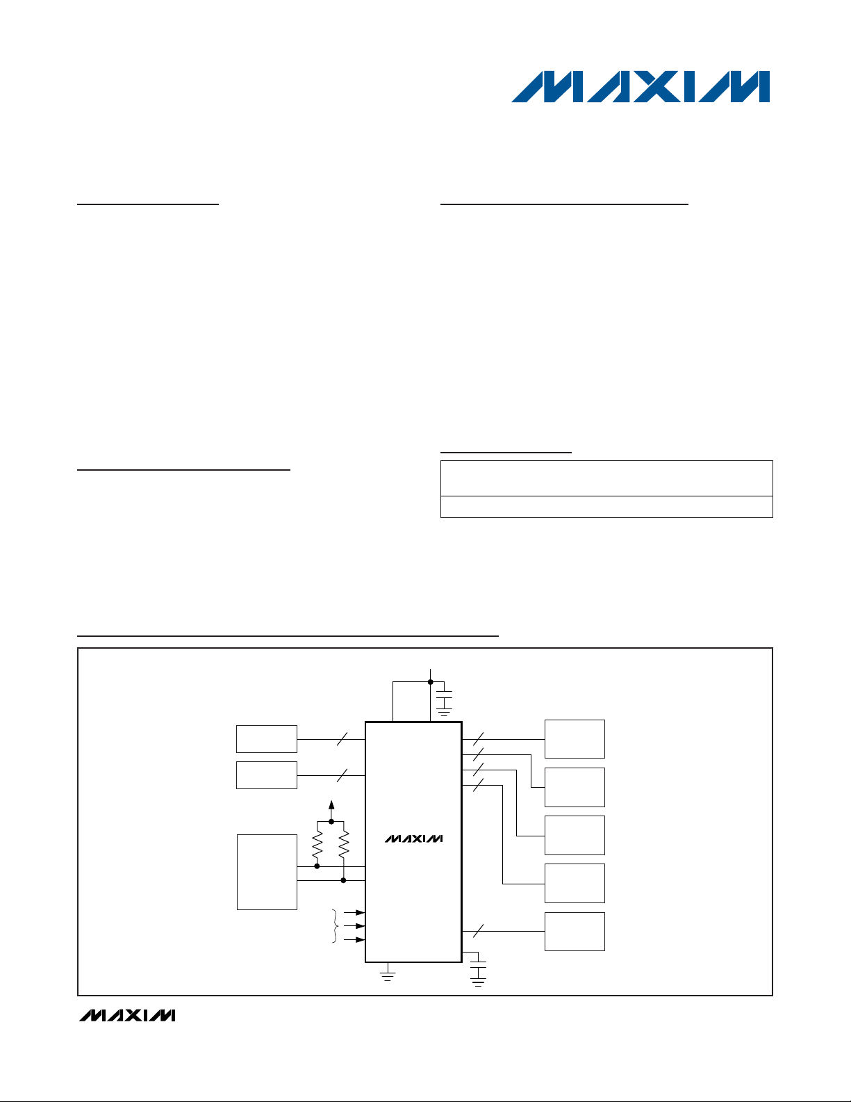
Typical I
2
C Operating Circuit
Pin Configuration appears at end of data sheet.
HDMI is a trademark of HDMI Licensing, LLC.
DVI is a trademark of Digital Display Working Group.
PART TEMP RANGE
PINPACKAGE
MAX4814EECB+ -40°C to +85°C 64 TQFP-EP* C64E-10
PKG
CODE
*SEE DEVICE ADDRESS SECTION.
DVI/HDMI 1
DVI/HDMI 2
μCONTROLLER
ADDRESS SELECTION*
4.5V TO 5.5V
0.1μF
V
MODE
5
A
5
B
V
DD
SCL
SDA
AD2
AD1
AD0
GND
MAX4814E
DD
SW0
SW1
SW2
SW3
EFN
5
5
5
5
4
DO
0.1μF
DVI/HDMI 1
OR
DVI/HDMI 2
DVI/HDMI 1
OR
DVI/HDMI 2
DVI/HDMI 1
OR
DVI/HDMI 2
DVI/HDMI 1
OR
DVI/HDMI 2
MAX3845
MAX4814E
DVI/HDMI 2:4 Low-Frequency Fanout Switch
2 _______________________________________________________________________________________
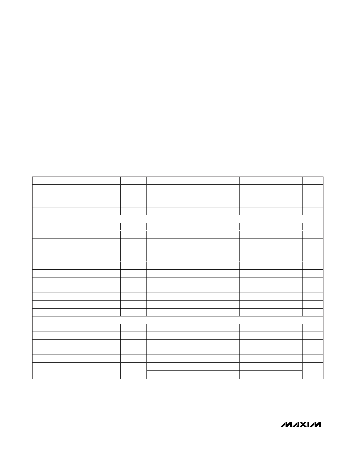
ABSOLUTE MAXIMUM RATINGS
ELECTRICAL CHARACTERISTICS
(VDD= +5V ±10%, TA= -40°C to +85°C, unless otherwise noted. Typical values are at TA= +25°C, VDD= +5V. Note 2.)
Stresses beyond those listed under “Absolute Maximum Ratings” may cause permanent damage to the device. These are stress ratings only, and functional
operation of the device at these or any other conditions beyond those indicated in the operational sections of the specifications is not implied. Exposure to
absolute maximum rating conditions for extended periods may affect device reliability.
(Voltages referenced to GND. Note 1.)
V
DD
, A_, B_, SW_, EFN..........................................-0.3V to +6.0V
All Other Pins (except GND).........................-0.3V to V
DD
+ 0.3V
Continuous Current, A_, B_ ..............................................±60mA
Continuous Current, V
DD
or GND...................................±100mA
Continuous Power Dissipation (T
A
= +70°C)
64-Pin TQFP (derate 31.3mW/°C above +70°C)........2508mW
Operating Temperature Range ...........................-40°C to +85°C
Junction Temperature......................................................+150°C
Storage Temperature Range .............................-65°C to +150°C
Lead Temperature (soldering) .........................................+300°C
Note 1: EFN must be either connected to VDDor left unconnected. EFN must not be connected to ground.
Power-Supply Voltage V
Power-Supply Current I
EFN Leakage Current I
LOGIC INPUTS (DA_, DB_, MODE, AD_)
Input Low Voltage DA_, DB_ V
Input High Voltage DA_, DB_ V
Input-Voltage Hysteresis DA_, DB_ V
Input Low Voltage AD_ V
Input High Voltage AD_ V
Input-Voltage Hysteresis AD_ V
Input Low Voltage MODE V
Input High Voltage MODE V
Input-Voltage Hysteresis MODE V
Input Leakage Current DA_, DB_ I
Input Leakage Current AD_ I
Input Leakage Current MODE I
LOGIC OUTPUTS DO_
Output-Voltage Low V
Output-Voltage High V
Output Leakage Current I
Output Rise Time t
Output Short-Circuit Current I
PARAMETER SYMBOL CONDITIONS MIN TYP MAX UNIT
DD
E FN = unconnected ; al l i np uts = 0;
DD
al l outp uts hi g h or l ow , no l oad s
V
L
IL
IH
HYST
IL
IH
HYST
IL
IH
HYST
L
L
L
OL
OH
L
R
SC
= VDD - 0.2V -2 +2 µA
EFN
MODE = 0V 0.8 V
MODE = 0V 2 V
MODE = 0V 150 mV
MODE = V
MODE = V
MODE = V
DD
DD
DD
MODE = 0V ±1 µA
MODE = V
MODE = VDD, I
MODE = VDD, I
M OD E = V
V
I N
V
OUT
I
SOURCE
I
SINK
DD
= 30µA 0.5 V
SINK
SOURCE
, outp ut at hi g h i m p ed ance,
D D
= 1.5V
from 0.8V to 2.2V, C
= 26µA 2 V
= 10pF 600 ns
LOAD
4.5 5 5.5 V
10 µA
0.8 V
2V
150 mV
0.8 V
2V
150 mV
±1 µA
±1 µA
±1 µA
-1
+3
mA
MAX4814E
DVI/HDMI 2:4 Low-Frequency Fanout Switch
_______________________________________________________________________________________ 3
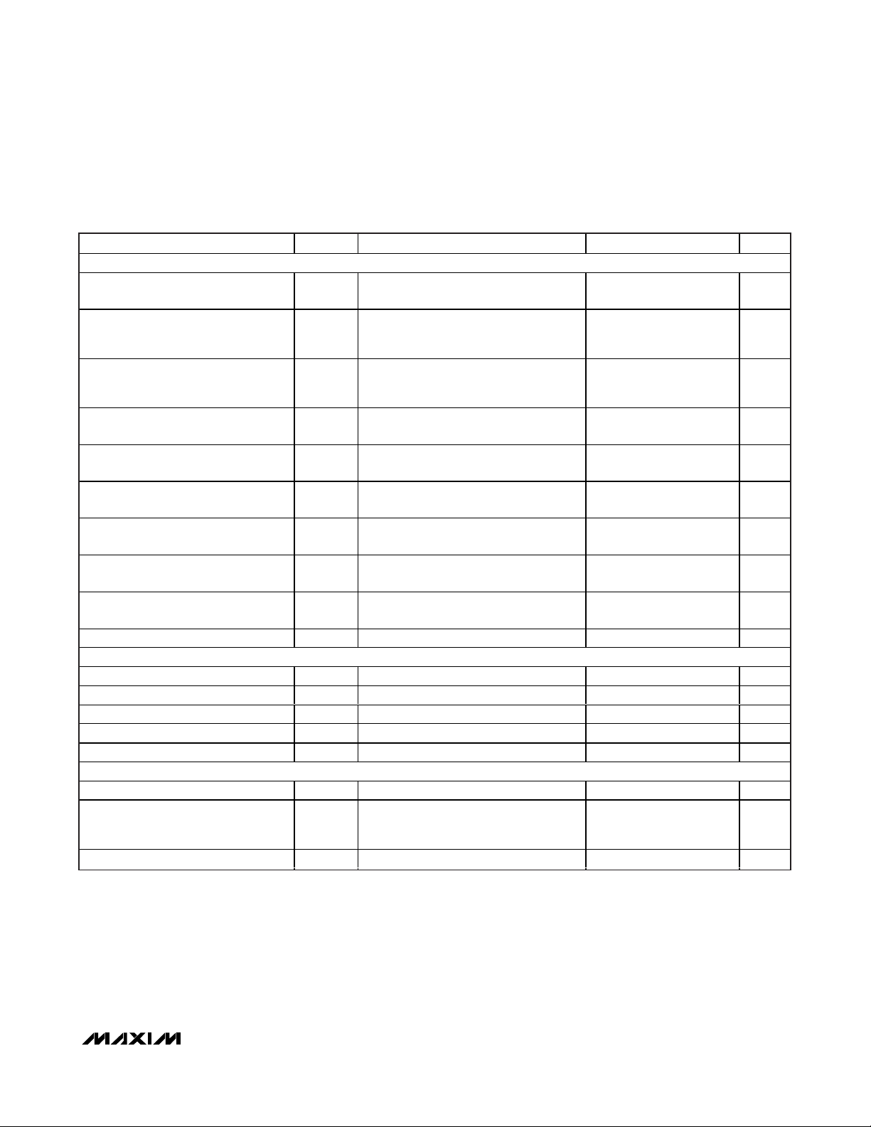
ELECTRICAL CHARACTERISTICS (continued)
(VDD= +5V ±10%, TA= -40°C to +85°C, unless otherwise noted. Typical values are at TA= +25°C, VDD= +5V. Note 2.)
ANALOG SWITCHES
On-Resistance Standard Switches:
A[1], A[2], A[3], B[1], B[2], B[3]
On-Resistance-Flatness Standard
Switches: A[1], A[2], A[3], B[1], B[2],
B[3]
On-Channel -3dB Bandwidth
Standard Switches: A[1], A[2], A[3],
B[1], B[2], B[3]
Off-Isolation Standard Switches: A[1],
A[2], A[3], B[1], B[2], B[3]
Crosstalk Standard Switches: A[1],
A[2], A[3], B[1], B[2], B[3]
On-Capacitance Standard Switches:
A[1], A[2], A[3], B[1], B[2], B[3]
Off-Capacitance Standard Switches:
A[1], A[2], A[3], B[1], B[2], B[3]
Charge Injection Q
On-Resistance +5V/Drain: A[0], A[4],
B[0], B[4]
Switch Leakage Current I
I2C SPECIFICATIONS (SDA, SCL, MODE = VDD)
Input Low Voltage V
Input High Voltage V
Input-Voltage Hysteresis V
Input Leakage Current I
Output-Voltage Low SDA V
TIMING CHARACTERISTICS (Figure 4), MODE = V
Serial Clock Frequency f
Hold Time (Repeated) START
Condition (after this period the first
clock pulse is generated)
Low Period of the SCL Clock t
PARAMETER SYMBOL CONDITIONS MIN TYP MAX UNIT
R
R
FLATVIN
BW
V
V
C
C
R
HYST
SCL
t
HD,STAfSCL
LOWfSCL
VIN = 2.5V, IIN = ±10mA 12 Ω
ON
= 0.8V, 2.5V, 3.7V 2.5 Ω
RS = RL = 50Ω, CL = 35pF, Figure 1 190 MHz
RS = RL = 50Ω, f = 1MHz, Figure 1 65 dB
ISO
RS = RL = 50Ω, f = 1MHz, Figure 1 75 dB
CT
VDD = 4.5V, f = 1MHz, Figure 2 37 pF
ON
VDD = 4.5V, f = 1MHz, Figure 2 15 pF
OFF
V
= 1.5V, R
GEN
Figure 3
VDD = 4.5V, VIN = 0V or V
ON
L
IL
IH
L
I
= 3mA 0.4 V
OL
SINK
DD
VDD = 4.5V 100 400 kHz
= 100kHz 4 µs
= 100kHz 4.7 µs
= 0Ω, CL = 100pF,
GEN
DD
13 pC
3 Ω
2.4 V
450 mV
±10 µA
0.8 V
±1 µA
MAX4814E
DVI/HDMI 2:4 Low-Frequency Fanout Switch
4 _______________________________________________________________________________________
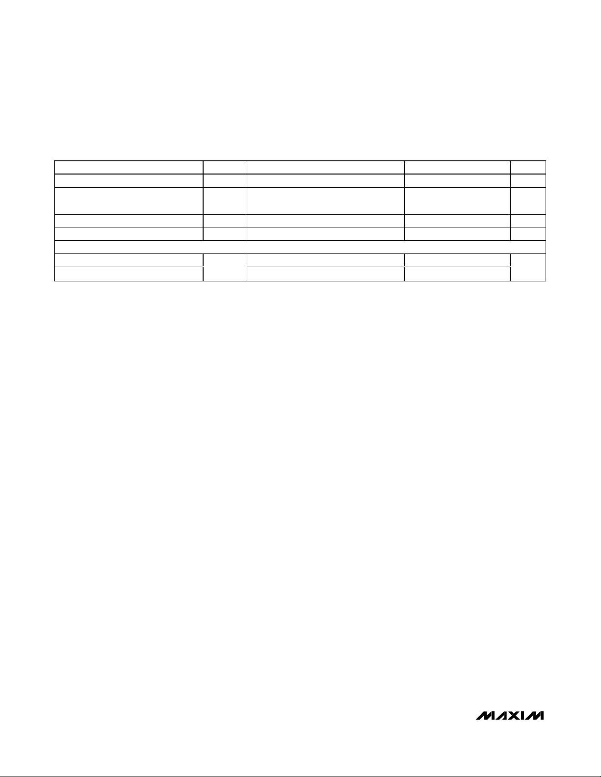
Note 2: Limits at TA= -40°C are guaranteed by design.
ELECTRICAL CHARACTERISTICS (continued)
(VDD= +5V ±10%, TA= -40°C to +85°C, unless otherwise noted. Typical values are at TA= +25°C, VDD= +5V. Note 2.)
High Period of the SCL Clock t
Setup Time for a Repeated START
Condition
Data Hold Time t
Data Setup Time t
ESD PROTECTION (HUMAN BODY MODEL)
SW_, A_, B_ Referenced to GND ±6
All Other I/Os
PARAMETER SYMBOL CONDITIONS MIN TYP MAX UNIT
HIGHfSCL
t
SU,STAfSCL
HD,DATfSCL
SU,DATfSCL
ESD
= 100kHz 4 µs
= 100kHz 4.7 µs
= 100kHz 25 µs
= 100kHz 250 ns
±2
kV
MAX4814E
DVI/HDMI 2:4 Low-Frequency Fanout Switch
_______________________________________________________________________________________ 5
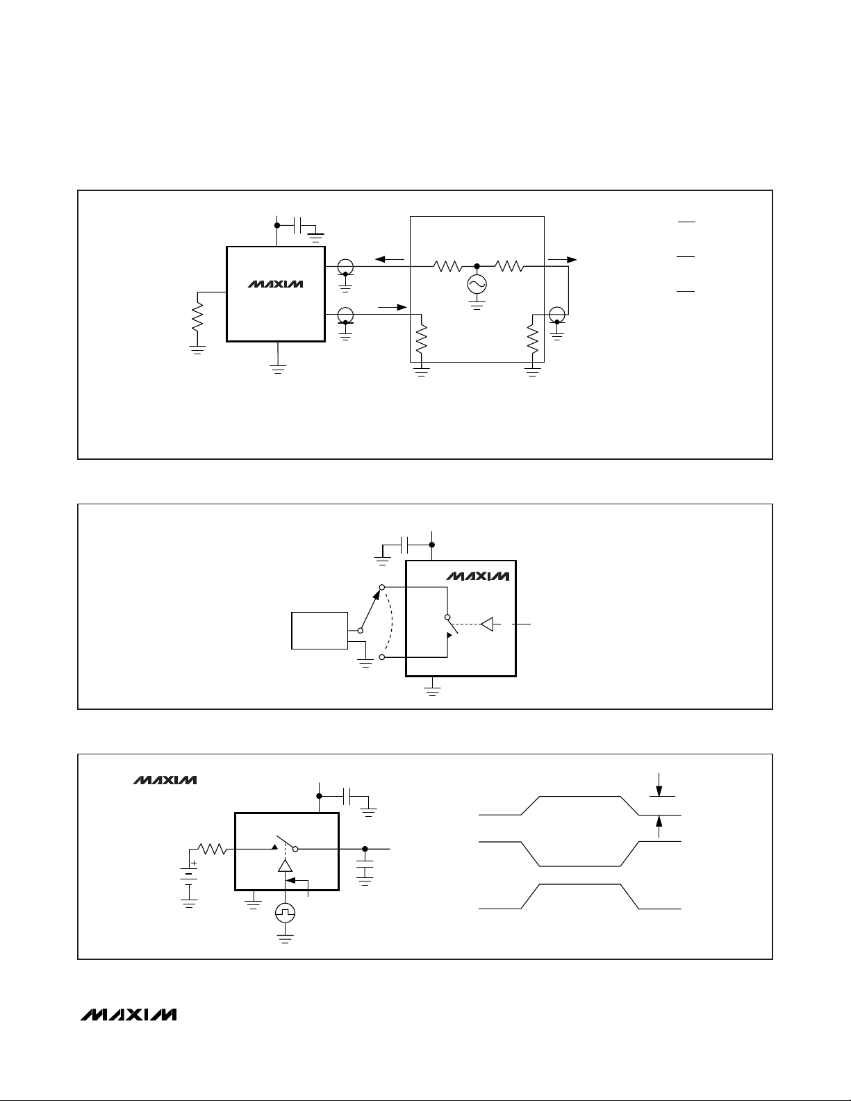
Figure 1. On-Loss, Off-Isolation, and Crosstalk
Figure 2. Channel Off-/On-Capacitance
Figure 3. Charge Injection
0.1μF
+5V
V
DD
B_
MAX4814E
50Ω
MEASUREMENTS ARE STANDARDIZED AGAINST SHORTS AT IC TERMINALS.
OFF-ISOLATION IS MEASURED BETWEEN SW_ AND "OFF" A_ OR B_ TERMINAL ON EACH SWITCH.
ON-LOSS IS MEASURED BETWEEN SW_ AND "ON" A_ OR B_TERMINAL ON EACH SWITCH.
CROSSTALK IS MEASURED FROM ONE CHANNEL TO ALL OTHER CHANNELS.
SIGNAL DIRECTION THROUGH SWITCH IS REVERSED; WORST VALUES ARE RECORDED.
SW_
GND
CAPACITANCE
METER
f = 1MHz
V
NETWORK
ANALYZER
V
A_
IN
V
OUT
0.1μF
50Ω
MEAS REF
50Ω 50Ω
+5V
V
DD
SW_
A_ OR
B_
MAX4814E
GND
DB_
DA_
SDA
SCL
50Ω
OR
V
IL
OR
V
IH
OFF-ISOLATION = 20log
ON-LOSS = 20log
CROSSTALK = 20log
OUT
V
IN
V
OUT
V
IN
V
OUT
V
IN
MAX4814E
R
GEN
A_
OR B_
V
GEN
GND
+5V
0.1μF
V
OUT
V
DD
SW_
DB_
SDA
OR
SCL
DA_
V
TO V
INL
INH
V
OUT
C
L
DB_
DA_
SDA
SCL
DB_
DA_
SDA
SCL
OR
OFF
OFF
OR
IN DEPENDS ON SWITCH CONFIGURATION;
INPUT POLARITY DETERMINED BY SENSE OF SWITCH.
Q = (ΔV
ON
ON
OUT
)(CL)
ΔV
OUT
OFF
OFF
MAX4814E
DVI/HDMI 2:4 Low-Frequency Fanout Switch
6 _______________________________________________________________________________________
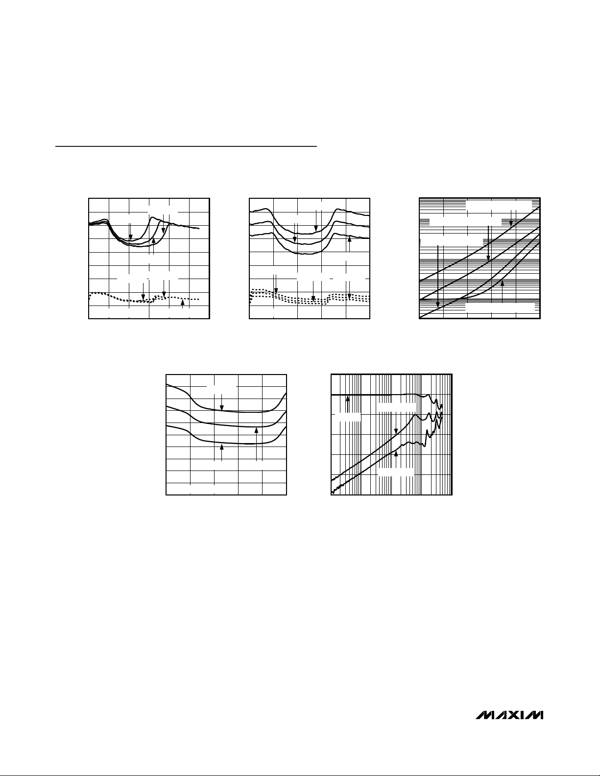
Typical Operating Characteristics
(VDD= +5V, TA= +25°C, unless otherwise noted.)
ON-RESISTANCE vs. VA OR V
18
16
14
12
10
8
6
ON-RESISTANCE (Ω)
4
2
0
021 3456
VDD = 4.5V
VDD = 5.0V
VDD = 4.5V
- - - - +5V/DRAIN
VA OR VB (V)
ON-RESISTANCE vs. VA OR V
18
16
14
12
10
8
TA = +85°C
6
4
2
- - - - +5V/DRAIN
0
021 345
VDD = 5.5V
VDD = 5.0V
B
MAX4814E toc01
ON-RESISTANCE (Ω)
VDD = 5.5V
SUPPLY CURRENT vs. TEMPERATURE
0.5
0.45
0.4
0.35
0.3
0.25
0.2
0.15
SUPPLY CURRENT (μA)
0.1
0.05
SWITCH I/O_ = 0V
0
-40 10-15 356085
VDD = 5.5V
VDD = 4.5V VDD = 5.0V
TEMPERATURE (°C)
TA = +25°C
TA = +25°C
VA OR VB (V)
MAX4814E toc04
B
TA = +85°C
TA = -40°C
TA = -40°C
100,000
10,000
MAX4814E toc02
LEAKAGE CURRENT (pA)
FREQUENCY RESPONSE
20
0
-20
ON-LOSS
-40
-60
FREQUENCY RESPONSE (dB)
-80
-100
0.1 1 100 1000
OFF-ISOLATION
CROSS-TALK
10
FREQUENCY (MHz)
LEAKAGE CURRENT vs. TEMPERATURE
+5V/DRAIN OFF-LEAKAGE
STD. SWITCH OFF-LEAKAGE
1000
+5V/DRAIN ON-LEAKAGE
100
10
1
0.1
-40 85
STD. SWITCH ON-LEAKAGE
10 35 60-15
TEMPERATURE (°C)
MAX4814E toc05
MAX4814E toc03
MAX4814E
DVI/HDMI 2:4 Low-Frequency Fanout Switch
_______________________________________________________________________________________ 7
Pin Description
PIN NAME FUNCTION
1, 16, 24, 25, 33, 48, 56, 57
GND Ground. Must connect all GND pins together.
2, 15, 34 I.C. Internally Connected. Leave I.C. unconnected
3 A[0] Switch A I/O 0. A[0] has a 3Ω (typ) resistance to switch 5V or drain.
4 A[1] Switch A I/O 1. A[1] has a 12Ω (typ) resistance to switch data.
5 A[2] Switch A I/O 2. A[2] has a 12Ω (typ) resistance to switch data.
6 A[3] Switch A I/O 3. A[3] has a 12Ω (typ) resistance to switch data.
7 A[4] Switch A I/O 4. A[4] has a 3Ω (typ) resistance to switch 5V or drain.
8, 9, 17, 32, 40, 41, 49, 64
V
DD
Positive-Supply Voltage Input. Connect VDD to a +5V supply voltage. Bypass VDD to
GND with a 0.1µF capacitor. Must connect all V
DD
pins together.
10 B[0] Switch B I/O 0. B[0] has a 3Ω (typ) resistance to switch 5V or drain.
11 B[1] Switch B I/O 1. B[1] has a 12Ω (typ) resistance to switch data.
12 B[2] Switch B I/O 2. B[2] has a 12Ω (typ) resistance to switch data.
13 B[3] Switch B I/O 3. B[3] has a 12Ω (typ) resistance to switch data.
14 B[4] Switch B I/O 4. B[4] has a 3Ω (typ) resistance to switch 5V or drain.
18 MODE
MODE Selection Input. Connect MODE to V
DD
(MODE = 1) to select I2C control mode.
Connect MODE to GND (MODE = 0) to select direct-control mode.
19 SDA I2C-Compatible Serial Data I/O
20 SCL I2C-Compatible Serial Clock Input
21 AD0
Programmable I
2
C Address Bit. AD[0] sets the I2C address of the device. User-
selectable device address bit, LSB, LSB+1, MSB (see Figure 5).
22 AD1
Programmable I
2
C Address Bit. AD[1] sets the I2C address of the device. User-
selectable device address bit, LSB, LSB+1, MSB (see Figure 5).
23 AD2
Programmable I
2
C Address Bit. AD[2] sets the I2C address of the device. User-
selectable device address bit, LSB, LSB+1, MSB (see Figure 5).
26
Switch 3 I/O 4
27
Switch 3 I/O 3
28
Switch 3 I/O 2
29
Switch 3 I/O 1
30
Switch 3 I/O 0
31, 50 EFN
ESD Protection. Connect EFN with an external 0.1µF capacitor to GND for ±15kV ESD
HBM protection. The capacitor from EFN to GND provides an additional discharge path
for the ESD energy.
35
Switch 2 I/O 4
36
Switch 2 I/O 3
37
Switch 2 I/O 2
38
Switch 2 I/O 1
39
Switch 2 I/O 0
42
Switch 1 I/O 4
43
Switch 1 I/O 3
44
Switch 1 I/O 2
SW3[4]
SW3[3]
SW3[2]
SW3[1]
SW3[0]
SW2[4]
SW2[3]
SW2[2]
SW2[1]
SW2[0]
SW1[4]
SW1[3]
SW1[2]

MAX4814E
DVI/HDMI 2:4 Low-Frequency Fanout Switch
8 _______________________________________________________________________________________
Detailed Description
The MAX4814E provides routing for low-frequency
DVI/HDMI signals. The MAX4814E is a bidirectional 2:4
DVI/HDMI switch. Each switch consists of five singlepole/single-throw (SPST) channels. The channels have a
low 3Ω (typ) on-resistance to route +5V and drain, and
three channels to route data. Channels A0, A4, B0, B4,
SW_0, and SW_4 have a 3Ω (typ) on-resistance to route
+5V and drain, and the remaining channels A1–A3,
B1–B3, SL0_3, and SW_1 have a 12Ω (typ) on-resistance to route data. The device features a mode input to
control the device using direct-control logic inputs or an
I2C interface. Connect MODE to GND to control the
device using the direct-control bits. Connect MODE to
VDDto control the device using I2C. In I2C mode, the
MAX4814E controls the MAX3845 (see Figure 5).
Analog Signal Levels
Signal inputs over the full voltage range (0V to VDD) are
passed through the switch with minimal change in onresistance (see the
Typical Operating Characteristics
).
The switches are bidirectional. Therefore, switch A_,
switch B_, and switch SW_ can be either inputs or outputs.
Switch Control
The MAX4814E features a mode input to control the
device through either an I2C interface or through directcontrol logic inputs. Connect MODE to GND (mode 0) to
control the device using the direct-control inputs DA_ and
DB_ (see Table 1 and Figure 6). Connect MODE to V
DD
(mode 1) to control the device using the I2C interface.
Direct Control Method (Mode 0)
In mode 0, DA0/DO0 becomes input DA0, DA1/DO1
Pin Description (continued)
PIN NAME FUNCTION
45
Switch 1 I/O 1
46
Switch 1 I/O 0
47 N.C. No Connection. Not internally connected.
51
Switch 0 I/O 4
52
Switch 0 I/O 3
53
Switch 0 I/O 2
54
Switch 0 I/O 1
55
Switch 0 I/O 0
58
Direct-Control Bit I/O. In mode 0, DA0/DO0 is set as an input, DA0, to control switch
connections. In mode 1, DA0/DO0 is set as an output, DO0. The output bits are used to
drive the MAX3845.
59
Direct-Control Bit I/O. In mode 0, DA1/DO1 is set as an input, DA1, to control switch
connections. In mode 1, DA1/DO1 is set as an output, DO1. The output bits are used to
drive the MAX3845.
60
Direct-Control Bit I/O. In mode 0 DA2/DO2 is set as an input, DA2, to control switch
connections. In mode 1, DA2/DO2 is set as an output, DO2. The output bits are used to
drive the MAX3845.
61
Direct-Control Bit I/O. In mode 0 DB0/DO3 is set as an input, DB0, to control switch
connections. In mode 1, DB0/DO3 is set as an output, DO3. The output bits are used to
drive the MAX3845.
62 DB1
Direct-Control Bit I/O. In mode 0, DB1 is set as an input. In mode 1, DB1 is high
impedance.
63 DB2
Direct-Control Bit I/O. In mode 0, DB2 is set as an input. In mode 1, DB2 is high
impedance.
EP EP
Exposed Pad. Connect exposed pad to ground. For enhanced thermal dissipation,
connect EP to a copper area as large as possible. Do not use EP as a sole ground
connection.
SW1[1]
SW1[0]
SW0[4]
SW0[3]
SW0[2]
SW0[1]
SW0[0]
DA0/DO0
DA1/DO1
DA2/DO2
DB0/DO3

becomes input DA1, DA2/DO2 becomes input DA2,
and DB0/DO3 becomes input DB0. Inputs DB1 and
DB2 are enabled.
In mode 0, the direct-control inputs DA_ and DB_ are
used to control the connection of the switches. DA2 is
used as the enable for switch A, and DB2 is used as the
enable for switch B. Connecting DA2 to VDDenables
switch A, and connecting DA2 to GND disables switch
A. Connecting DB2 to VDDenables switch B, and connecting DB2 to GND disables switch B. Inputs DA0 and
MAX4814E
DVI/HDMI 2:4 Low-Frequency Fanout Switch
_______________________________________________________________________________________ 9
Functional Diagram
V
A_
B_
5
5
B0
B1
B2
B3
A0
A1
A2
A3
B_
DECODER
MUX
MAX4814E
A_
6
6
DO[3:0]
4
HI-Z
DB0
DA_
6
4
DD
5
SW0_
5
SW1_
5
SW2_
5
SW3_
I2C SERIAL PORT AND REGISTERS
GND
446
I.C.
N.C.
EFN
ENENENENEN
AD2AD1AD0SCLSDAMODE
DB_
DA_

MAX4814E
DA1 select the connections of switch A to switch SW_
and inputs DB0 and DB1. Select the connections of
switch B to SW_. See Table 3a for the pin configuration
and Table 3b for a complete summary.
I2C Interface Method (Mode 1)
In mode 1, the switch connections are controlled
through the I2C interface. Inputs SDA and SCL program
registers R0 and R1. Register R0, bits [7 to 2], select
the connection of switch A and switch B to switch SW_
(see the
I2C Registers and Bit Descriptions
section).
The bits of register R1 transfer data to the output DO_.
The data on output DO_ is used to communicate with the
MAX3845. In mode 1, DA0/DO0 becomes output DO0,
DA1/DO1 becomes output DO1, DA2/DO2 becomes
output DO2, and DB0/DO3 becomes output DO3. DB1
and DB2 are high impedance. See Table 3a for the pin
configuration. See Table 4 for register R1 to DO_ output
mapping.
I2C Registers and Bit Descriptions
Two internal registers (RO and R1) program the
MAX4814E. Table 2 lists both registers, their addresses, and power-up default states. Both registers are
read/write registers.
In register R0, bit BAEN is used as the enable for
switch A, and bit BBEN is used as the enable for switch
B. Writing 1 to bit BAEN enables switch A; and writing 0
to bit BAEN disables switch A. Writing 1 to bit BBEN
enables switch B, and writing 0 to bit BBEN disables
switch B. BASEL1 and BASEL0 select the connections
of switch A to switch SW_, while BBSEL1 and BBSEL0
select the connections of switch B to switch SW_, as
summarized in Table 6.
I2C Register R0 Two LSB Bits
The two LSBs are hard coded as 00. Register R0
ignores any value written to the two LSBs; anytime register R0 is read the hard-coded values are returned.
Bank A Enable (BAEN) and Bank B Enable (BBEN) Bits
1 = Enable
0 = Disable
Bank A Select (BASEL1/BASEL0) and
Bank B Select (BBSEL1/BBSEL0) Bits
Bits BASEL1 and BASEL0 select the switch SW_ that
switch A is connected to. Bits BBSEL1 and BBSEL0
select the switch SW_ that switch B is connected to
(see Table 6).
Power-On Default States
When power is applied to the MAX4814E internal
power-on reset (POR), circuitry sets registers R0 and
R1 to their default states. Register R0 is set to all zeros,
or 00h, and register R1 is set to 10101010, or AAh, as
shown in Table 2.
Having all zeros in register R0 disables both banks A
and B; see Table 6 for register R0 to switch mapping.
Setting register R1 to AAh forces the outputs at DO_ to
be high impedance.
Note: The output, DO_ is used to communicate with the
MAX3845 when the MAX4814E is being used without its
companion. The MAX3845 and the MAX4814E use the
I2C interface (MODE = 1). All DO_ outputs need to be
connected through a 10kΩ resistor to GND.
DVI/HDMI 2:4 Low-Frequency Fanout Switch
10 ______________________________________________________________________________________
X = Hardwired code, not programmable by user.
Table 1. Mode Configuration
Table 2. I2C Register Map
INPUT PIN
MODE
0 Puts the device in mode 0. The direct-control inputs DA_ and DB_ control the switches.
1
P uts the d evi ce i n m od e 1. The sw i tches ar e contr ol l ed b y the I
Inp uts D B1 and D B2 ar e hi g h i m p ed ance.
OPERATION
2
C i nter face. D O _ b ecom es an acti ve outp ut.
REGISTER
R0 BBEN
R1
76543210
D O3
H i g h
Im p ed ance
BBSE
L1
DO3
Data
BBSEL0 BAEN BASEL1
DO2
High
Im p ed ance
BIT POWER-UP
DO2
Data
DO1
High
Im p ed ance
BASE
L0
DO1
Data
X X 0x00
DO0
High
Im p ed ance
DO0
Data
ADDRESS
0x01
BINARY HEX
0000
0000
1010
1010
00
AA

I2C Interface
The MAX4814E features an I2C interface using a
repeated start. The MAX4814E I2C interface refers to
the I2C bus specification (version 2.1, Jan 2000).
Device Address
The MAX4814E has selectable device addresses
through external inputs. The slave address consists of
four fixed bits (B7–B4, set to 0111) followed by three pinprogrammable bits (AD2–AD0), as shown on Table 7.
MAX4814E
DVI/HDMI 2:4 Low-Frequency Fanout Switch
______________________________________________________________________________________ 11
Table 3a. Input/Output Configurations for DA_, DB_, and DO_
Table 3b. Mode 0 Direct-Control Configurations
Note: When switch A and switch B are connected to the same SW_, switch A takes precedence and switch B is high impedance.
MODE
0 DA0, Input DA1, Input DA2, Input DB0, Input DB1, Input DB2, Input
1 DO0, Output DO1, Output DO2, Output DO3, Output High Impedance High Impedance
DA0/DO0 DA1/DO1 DA2/DO2 DB0/DO3 DB1 DB2
PIN CONFIGURATION
PIN CONNECTION
DA2
0 Bank A switches are disabled
1 Bank A switches are enabled. Switch A connections depend on the DA0 and DA1 inputs.
PIN CONNECTION
DB2
0 Bank B switches are disabled
1 Bank B switches are enabled. Switch B connections depend on the DB0 and DB1 inputs.
PIN CONNECTION
DB1 DB0 DA1 DA0
0 0 0 0 Connect A to SW0 B is high impedance
0 0 0 1 Connect A to SW1 Connect B to SW0
0 0 1 0 Connect A to SW2 Connect B to SW0
0 0 1 1 Connect A to SW3 Connect B to SW0
0 1 0 0 Connect A to SW0 Connect B to SW1
0 1 0 1 Connect A to SW1 B is high impedance
0 1 1 0 Connect A to SW2 Connect B to SW1
0 1 1 1 Connect A to SW3 Connect B to SW1
1 0 0 0 Connect A to SW0 Connect B to SW2
1 0 0 1 Connect A to SW1 Connect B to SW2
1 0 1 0 Connect A to SW2 B is high impedance
1 0 1 1 Connect A to SW3 Connect B to SW2
1 1 0 0 Connect A to SW0 Connect B to SW3
1 1 0 1 Connect A to SW1 Connect B to SW3
1 1 1 0 Connect A to SW2 Connect B to SW3
1 1 1 1 Connect A to SW3 B is high impedance
OPERATION
OPERATION
OPERATION

MAX4814E
For example: If AD0, AD1, and AD2 are hardwired to
ground, then the complete address is 0111000. The full
address is defined as the seven most significant bits
followed by the read/write bit. Set the read/write bit to 1
to configure the MAX4814E to read mode. Set the
read/write bit to 0 to configure the MAX4814E to write
mode. The address is the first byte of information sent
to the MAX4814E after the START condition.
.
Applications Information
ESD Protection
As with all Maxim devices, ESD-protection structures
are incorporated on all pins to protect against electrostatic discharges encountered during handling and
assembly. Switch A, switch B, and switch SW_ are further protected against static electricity. Maxim’s engineers have developed state-of-the-art structures to
protect these pins against ESD up to ±6kV without
damage. The ESD structures withstand high ESD in
normal operation, and when the device is powered
down. ESD protection can be tested in various ways.
The ESD protection of switch A, switch B, and switch
SW_ are characterized for ±6kV (Human Body Model)
using the MIL-STD-883.
ESD Test Conditions
ESD performance depends on a variety of conditions.
Contact Maxim for a reliability report that documents
test setup, test methodology, and test results.
Human Body Model
Figure 7 shows the Human Body Model, and Figure 8
shows the current waveform it generates when discharged into a low impedance. This model consists of a
100pF capacitor charged to the ESD voltage of interest
that is then discharged into the test device through a
1.5kΩ resistor.
DVI/HDMI 2:4 Low-Frequency Fanout Switch
12 ______________________________________________________________________________________
Table 4. I2C Register R1 (0X01) to DO_ Mapping
Table 5. I2C Register R0 (0x00)
X = Hardwired, not programmed by user.
X = Don’t care.
PIN REGISTER R1 (0x01)
MODE BIT 7 BIT 6 BIT 5 BIT 4 BIT 3 BIT 2 BIT 1 BIT 0
1 — — — — — — 0 0 DO0 0
1 — — — — — — 0 1 DO0 1
1 — — — — — — 1 X DO0 Hi-Z
1————0 0——DO10
1————0 1——DO11
1 — — — — 1 X — — DO1 Hi-Z
1——0 0————DO20
1——0 1————DO21
1 — — 1 X — — — — DO2 Hi-Z
100——————DO30
101——————DO31
1 1 X — — — — — — DO3 Hi-Z
CONFIGURATION
OUTPUT PIN
REGISTER R0 (0x00)
BIT 7 BIT 6 BIT 5 BIT 4 BIT 3 BIT 2 BIT 1 BIT 0
BBEN BBSEL1 BBSEL0 BAEN BASEL1 BASEL0 X X

Power-Supply Biasing and Sequencing
Proper power-supply sequencing is recommended for
all CMOS devices. Do not exceed the absolute maximum ratings, since stresses beyond the listed ratings
can cause permanent damage to the device. Always
sequence V
DD
on first, followed by the switch inputs
and the logic inputs. Bypass at least one VDDinput to
ground with a 0.1µF capacitor as close as possible to
the device. Use the smallest physical size possible for
optimal performance.
MAX4814E
DVI/HDMI 2:4 Low-Frequency Fanout Switch
______________________________________________________________________________________ 13
Table 6. Switch Selection Truth Table
— = Denotes no connection.
1 = Denotes switch connection.
0 = Denotes switch B is high impedance.
X = Don’t care.
Table 7. MAX4814E Device Address
DA_, DB_ INPUTS/REGISTER R0 BITS SWITCH A AND B TO SW_ CONNECTIONS
DB2/
BBEN
0 X X 0 X X ————————
0 X X 1 0 0 ——————— 1
0 X X 1 0 1 —————— 1 —
0 X X 1 1 0 ————— 1 ——
0 X X 1 1 1 ———— 1 ———
1 0 0 0 X X ——— 1 ————
1 0 0 1 0 0 ——— 0 ——— 1
10 010 1 ———1——1—
10 011 0 ———1—1——
1 0 0 1 1 1 ——— 1 1 ———
1 0 1 0 X X —— 1 —————
1 0 1 1 0 0 —— 1 ———— 1
1 0 1 1 0 1 —— 0 ——— 1 —
10 111 0 ——1——1——
1 0 1 1 1 1 —— 1 — 1 ———
1 1 0 0 X X — 1 ——————
1 1 0 1 0 0 — 1 ————— 1
1 1 0 1 0 1 — 1 ———— 1 —
11 011 0 —0———1——
1 1 0 1 1 1 — 1 —— 1 ———
1 1 1 0 X X 1 ———————
1 1 1 1 0 0 1 —————— 1
1 1 1 1 0 1 1 ————— 1 —
1 1 1 1 1 0 1 ———— 1 ——
1 1 1 1 1 1 0 ——— 1 ———
DB1/
BBSEL1
DB0/
BBSEL0
DA2/
BAEN
DA1/
BASEL1
DA0/
BASEL0
B TO
SW3
B TO
SW2
B TO
SW1
B TO
SW0
A TO
SW3
A TO
SW2
A TO
SW1
A TO
SW0
B7 B6 B5 B4 B3 B2 B1 B0
0 1 1 1 AD2 AD1 AD0 R/W
Fixed User Selected —

MAX4814E
DVI/HDMI 2:4 Low-Frequency Fanout Switch
14 ______________________________________________________________________________________
Figure 4. 2-Wire Interface Timing Diagram
Figure 5. Mode 1: I2C Control
Figure 6. Mode 0: Direct Control
Figure 7. Human Body ESD Test Model
Figure 8. Human Body Current Waveform
SDA
SCL
2
MODE = 1: I
V
DD
I2C CONTROL
C CONTROL
MAX4814E MAX3845
2223 211918 20
SDA SCL
3-STATE
CONTROL
58
59
60
61
SETS 3 LSBs OF I
AS SHOWN ADDRESS = 0111 + LSB = 0111000.
THERE ARE 8 POSSIBLE I
BY HARDWIRING PINS 23, 22, AND 21 TO 1 OR 0 USER
CAN CHANGE ADDRESS.
SEE TABLE 4 FOR I
t
HD, STA
START
CONDITION
96
65
61
30
2
C ADDRESS.
2
2
C REGISTERS.
t
LOW
C ADDRESSES.
t
SU, DAT
t
HD, DAT
t
HIGH
t
r
t
f
t
SU, STA
REPEATED
START CONDITION
MODE = 0: DIRECT CONTROL
MAX4814E
21
18
MODE = 0
SEE TABLE 3b FOR CONTROL FUNCTIONS.
23
DA022DA161DB0
DA2
62
DB163DB2
R
D
1500Ω
DISCHARGE
RESISTANCE
STORAGE
CAPACITOR
HIGH-
VOLTAGE
DC
SOURCE
R
C
1MΩ
CHARGE-CURRENT-
LIMIT RESISTOR
C
100pF
s
DEVICE
UNDER
TEST
AMPERES
IP 100%
90%
36.8%
10%
0
0
t
RL
I
r
TIME
t
DL
CURRENT WAVEFORM
PEAK-TO-PEAK RINGING
(NOT DRAWN TO SCALE)

MAX4814E
DVI/HDMI 2:4 Low-Frequency Fanout Switch
______________________________________________________________________________________ 15
It is also recommended to bypass more than one V
DD
input. A good strategy is to bypass one VDDinput with
a 0.1µF capacitor and at least a second VDDinput with
a 1nF to 10nF capacitor (use a 0603 or smaller physical
size ceramic capacitor).
Chip Information
PROCESS: BiCMOS
Pin Configuration
58
59
60
61
62
54
55
56
57
63
38394041424344454647
DA1/DO1
A[0]
N.C.
TQFP
SW1[0]
SW1[1]
SW1[2]
SW1[3]
SW1[4]
VDDV
DD
SW2[0]
SW2[1]
52
53
49
50
51
SW2[2]
SW2[3]
SW2[4]
I.C.
GND
I.C.
A[2]
A[1]
A[4]
A[3]
VDDV
DD
B[1]
B[0]
B[3]
B[2]
I.C.
B[4]
GND
EFN
SW3[0]
SW3[1]
SW3[2]
SW3[3]
SW3[4]
GND
GND
AD2
AD1
3334353637
AD0
SCL
SDA
MODE
V
DD
DA0/DO0
GND
GND
SW0[0]
SW0[1]
V
DD
DB2
DB1
DB0/DO3
DA2/DO2
SW0[2]
SW0[3]
SW0[4]
EFN
48
V
DD
V
DD
64
GND
GND
23
22
21
20
19
27
26
25
24
18
29
28
32
31
30
17
11109876543216151413121
MAX4814E
TOP VIEW
*CONNECT EXPOSED PADDLE TO GND.
*EP

MAX4814E
DVI/HDMI 2:4 Low-Frequency Fanout Switch
16 ______________________________________________________________________________________
Package Information
(The package drawing(s) in this data sheet may not reflect the most current specifications. For the latest package outline information,
go to www.maxim-ic.com/packages
.)
64L, TQFP.EPS
PACKAGE OUTLINE,
64L TQFP, 10x10x1.0mm EP OPTION
21-0084
1
C
2

MAX4814E
DVI/HDMI 2:4 Low-Frequency Fanout Switch
Maxim cannot assume responsibility for use of any circuitry other than circuitry entirely embodied in a Maxim product. No circuit patent licenses are
implied. Maxim reserves the right to change the circuitry and specifications without notice at any time.
Maxim Integrated Products, 120 San Gabriel Drive, Sunnyvale, CA 94086 408-737-7600 ____________________
17
© 2007 Maxim Integrated Products is a registered trademark of Maxim Integrated Products, Inc.
SPRINGER
Package Information (continued)
(The package drawing(s) in this data sheet may not reflect the most current specifications. For the latest package outline information,
go to www.maxim-ic.com/packages
.)
PACKAGE OUTLINE,
64L TQFP, 10x10x1.0mm EP OPTION
21-0084
2
C
2
 Loading...