

Page 1
General Description
The MAX4800A/MAX4802A provide high-voltage switching on eight channels for ultrasonic imaging and printer
applications. The devices utilize BCDMOS process technology to provide eight high-voltage low-charge-injection
SPST switches, controlled by a 20MHz serial interface.
Data is clocked into an internal 8-bit shift register and
retained by a programmable latch with enable and clear
inputs. A power-on reset function ensures that all switches are open on power-up.
The MAX4800A/MAX4802A operate with a wide range
of high-voltage supplies including: V
PP/VNN
= +100V/
-100V, +185V/-15V, and +40V/-160V. The digital interface operates from a separate V
DD
supply from +2.7V
to +6V. Digital inputs DIN, CLK, LE, and CLR are +6V
tolerant, independent of the VDDsupply voltage. The
MAX4802A provides integrated 35kΩ bleed resistors on
each switch terminal to discharge capacitive loads.
The MAX4800A/MAX4802A are drop-in replacements for
the Supertex HV2203 and HV2303. The devices are available in the 48-pin TQFP, 26-bump CSBGA, and 28-pin
PLCC packages. All devices are specified for the commercial 0°C to +70°C temperature range.
Applications
Ultrasound Imaging
Printers
Features
♦ Fast SPI™ Interface 20MHz
♦ Pin-Compatible Replacement for Supertex HV2203
(MAX4800A)
♦ Pin-Compatible Replacement for Supertex HV2303
(MAX4802A)
♦ Flexible High-Voltage Supplies Up to V
PP
- VNN= 200V
♦ Low-Charge-Injection, Low-Capacitance 22
ΩΩ
Switches
♦ DC to 10MHz Analog-Signal Frequency Range
♦ -77dB Off-Isolation at 5MHz
♦ Low 10µA Quiescent Current
♦ Integrated Bleed Resistors (MAX4802A Only)
♦ Available in Standard PLCC, TQFP, and CSBGA
Packages
MAX4800A/MAX4802A
Low-Charge-Injection, 8-Channel, High-Voltage
Analog Switches with 20MHz Serial Interface
________________________________________________________________
Maxim Integrated Products
1
19-4120; Rev 0; 5/08
For pricing, delivery, and ordering information, please contact Maxim Direct at 1-888-629-4642,
or visit Maxim’s website at www.maxim-ic.com.
Ordering Information/
Selector Guide
PART
BLEED
SECOND
SOURCE
PIN-
PACKAGE
MAX4800ACXZ+*
No —
26 CSBGA
MAX4800ACQI+ No
28 PLCC
MAX4800ACCM+*
No
48 TQFP
MAX4802ACXZ+*
Yes —
26 CSBGA
MAX4802ACQI+ Yes
28 PLCC
MAX4802ACCM+*
Yes
48 TQFP
Note: All devices are specified over the commercial 0°C to +70°C
temperature range.
*
Future product—contact factory for availability.
+
Denotes a lead-free package.
SPI is a trademark of Motorola, Inc.
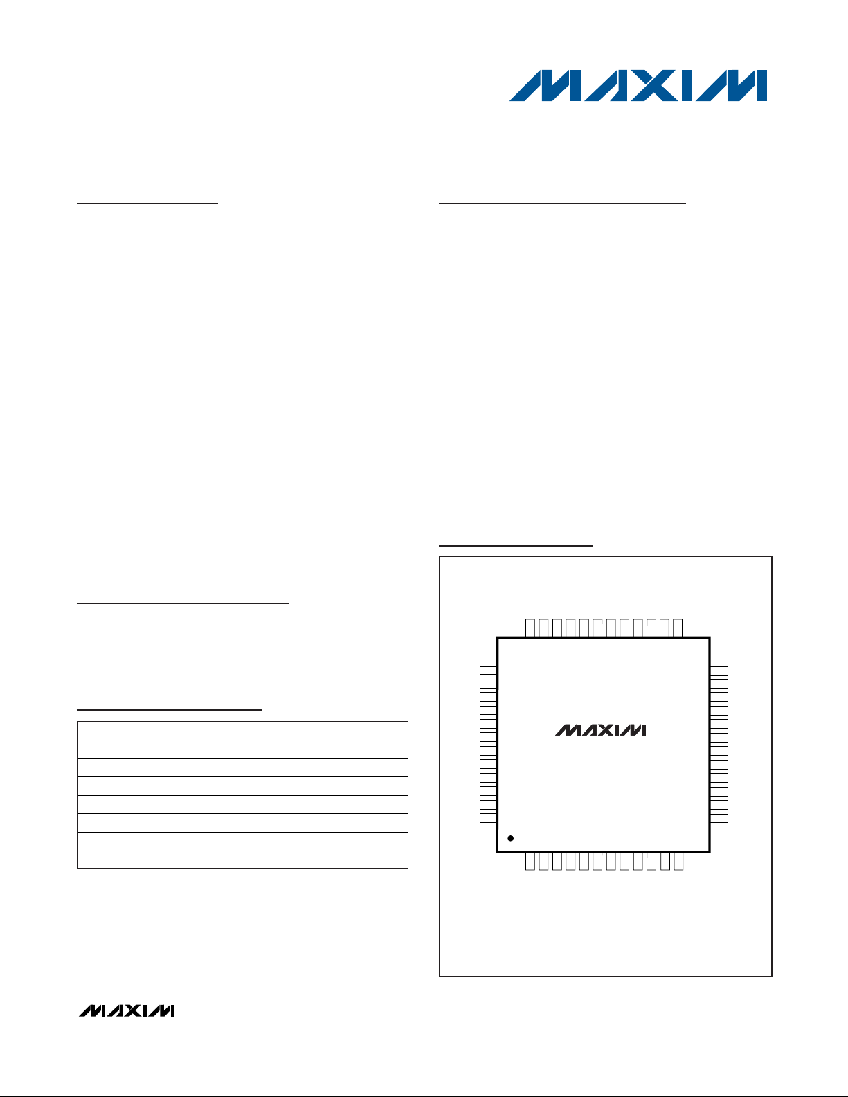
CLR
LE
DIN
N.C.
V
DD
GND
N.C. (RGND)
N.C.
V
NN
N.C.
N.C.
CLK
COM4
N.C.
NO4
N.C.
N.C.
COM3
N.C.
COM2
NO3
N.C.
N.C.
COM5
N.C.
NO1
N.C.
N.C.
V
PP
N.C.
NO0
COM1
N.C.
NO2
N.C.
NO5
N.C.
NO6
N.C.
COM6
N.C.
NO7
N.C.
COM7
DOUT
N.C.
N.C.
MAX4800A
MAX4802A
COM0
() MAX4802A ONLY
1234 5678
9
101112
363534 33 32 313029
28
272625
37
38
39
40
41
42
43
44
45
46
47
48
24
23
22
21
20
19
18
17
16
15
14
13
TQFP
7mm x 7mm
TOP VIEW
Pin Configurations
Pin Configurations continued at end of data sheet.
HV2203PJ-G
HV2203FG-G
HV2303PJ-G
HV2303FG-G
RESISTORS
Page 2
MAX4800A/MAX4802A
Low-Charge-Injection, 8-Channel, High-Voltage
Analog Switches with 20MHz Serial Interface
2 _______________________________________________________________________________________
ABSOLUTE MAXIMUM RATINGS
Stresses beyond those listed under “Absolute Maximum Ratings” may cause permanent damage to the device. These are stress ratings only, and functional
operation of the device at these or any other conditions beyond those indicated in the operational sections of the specifications is not implied. Exposure to
absolute maximum rating conditions for extended periods may affect device reliability.
(All voltages referenced to GND.)
V
DD
Logic Supply Voltage........................................-0.3V to +7V
V
PP
- VNNSupply Voltage ....................................................220V
V
PP
Positive Supply Voltage......................-0.3V to (VNN+ 220V)
V
NN
Negative Supply Voltage ..............................+0.3V to -220V
Logic Inputs LE, CLR, CLK, DIN ..............................-0.3V to +7V
DOUT..........................................................-0.3V to (V
DD
+ 0.3V)
RGND (MAX4802A)...............................................-4.5V to +0.3V
COM_, NO_.................................................................V
NN
to V
PP
Continuous Power Dissipation (TA= +70°C)
26-Bump CSBGA (derate 11.8mW/°C above +70°C)..941mW
28-Pin PLCC (derate 10.5mW/°C above +70°C) .........842mW
48-Pin TQFP (derate 22.7mW/°C above +70°C)........1818mW
Junction-to-Case Thermal Resistance (
θ
J
C
) (Note 1)
26-Lead CSBGA ........................................................ 23°C/W
28-Lead PLCC .............................................................10°C/W
48-Lead TQFP .............................................................10°C/W
Junction-to-Ambient Thermal Resistance (
θ
J
A
) (Note 1)
26-Lead CSBGA ........................................................ 85°C/W
28-Lead PLCC .............................................................44°C/W
48-Lead TQFP .............................................................44°C/W
Operating Temperature Range...............................0°C to +70°C
Storage Temperature Range .............................-65°C to +150°C
Junction Temperature......................................................+150°C
Lead Temperature (Soldering, 10s).................................+300°C
Bump Temperature Lead-Free (Soldering)......................+260°C
Bump Temperature Lead (Soldering) ..............................+245°C
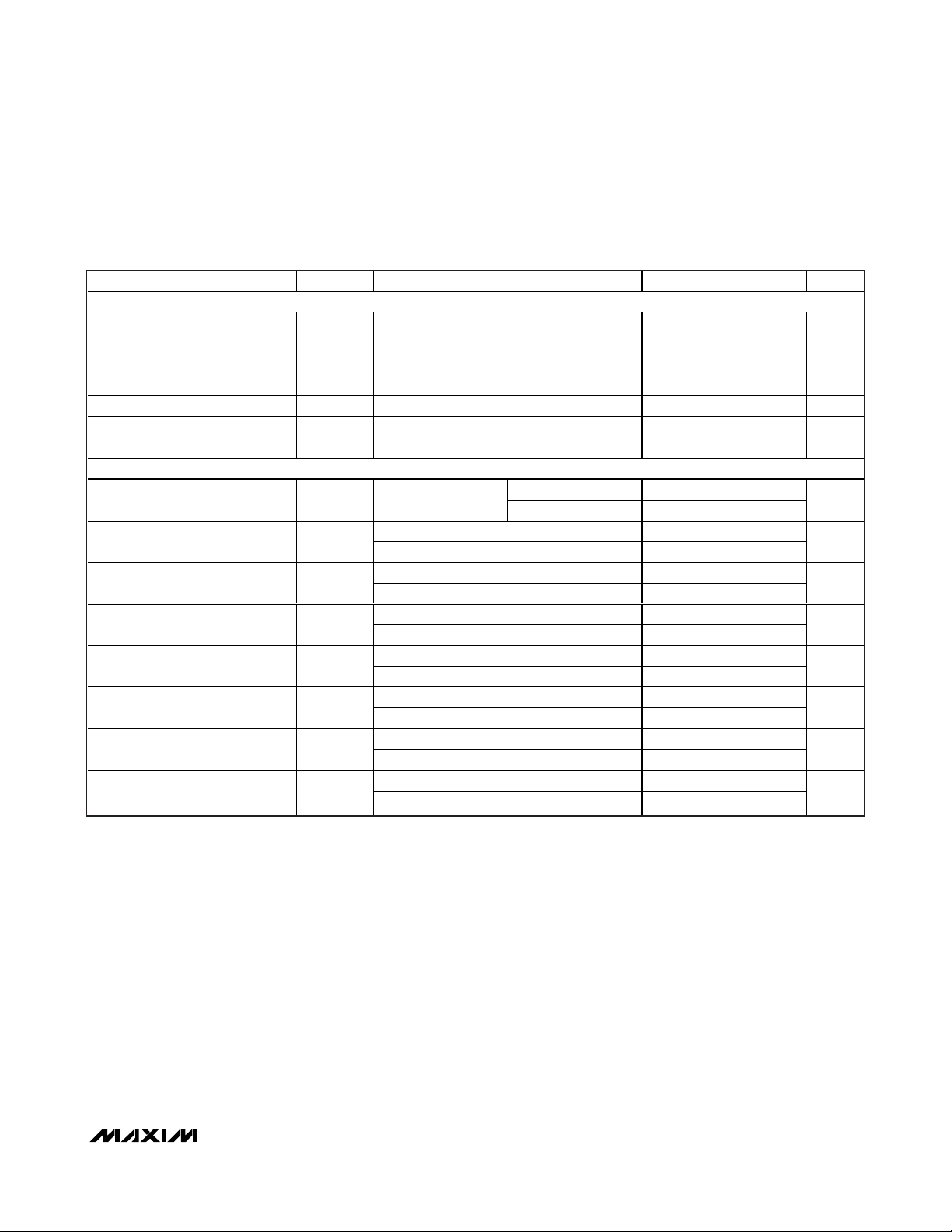
ELECTRICAL CHARACTERISTICS
(VDD= +2.7V to +6V, VPP= +40V to (VNN+ 200V), VNN= -40V to -160V, TA= T
MIN
to T
MAX
, unless otherwise noted. Typical values
are at T
A
= +25°C.) (Note 2)
PARAMETER
SYMBOL
CONDITIONS
MIN
TYP
MAX
UNITS
ANALOG SWITCH
Analog Signal Range
V
COM_
,
V
NO_
(Note 3)
V
NN
+
10
V
PP
-
10
V
TA = 0°C 30
26 38I
COM
= 5mA
48
TA = 0°C 25
22 27
V
COM_
= 0
I
COM
=
200mA
32
TA = 0°C 25
22 27I
COM
= 5mA
30
TA = 0°C 18
18 24
V
C OM _
= 0
I
COM
=
200mA
27
TA = 0°C 23
20 25
I
COM
= 5mA
30
TA = 0°C 22
16 25
Small-Signal Switch
On-Resistance
R
ONS
V
N N
= - 40V
I
COM
=
200mA
27
Ω
Note 1: Package thermal resistances were obtained using the method described in JEDEC specification JESD51-7, using a 4-layer
board. For detailed information on package thermal considerations, refer to www.maxim-ic.com/thermal-tutorial
.
V
= +40V,
PP
= -160V,
V
NN
V
= + 100V ,
P P
= - 100V ,
V
N N
V
= + 160V ,
P P
TA = +25°C
TA = +70°C
TA = +25°C
TA = +70°C
TA = +25°C
TA = +70°C
TA = +25°C
TA = +70°C
TA = +25°C
TA = +70°C
TA = +25°C
TA = +70°C
Page 3
MAX4800A/MAX4802A
Low-Charge-Injection, 8-Channel, High-Voltage
Analog Switches with 20MHz Serial Interface
_______________________________________________________________________________________ 3
ELECTRICAL CHARACTERISTICS (continued)
(VDD= +2.7V to +6V, VPP= +40V to (VNN+ 200V), VNN= -40V to -160V, TA= T
MIN
to T
MAX
, unless otherwise noted. Typical values
are at T
A
= +25°C.) (Note 2)
PARAMETER
CONDITIONS
UNITS
Small-Signal Switch
On-Resistance Matching
ΔR
ONS
V
P P
= + 100V , V
N N
= - 100V ,
V
COM_
= 0, I
COM
= 5mA
520%
Large-Signal Switch
On-Resistance
R
ONL
V
COM_
= V
PP
- 10V, I
COM
= 1A 15 Ω
Shunt Resistance
(MAX4802A only)
R
INT
NO_ or COM_ to RGND, switch off 30 35 50 kΩ
02
Switch-Off Leakage
),
)
V
COM_
, V
NO_
= VPP - 10V or unconnected;
(MAX4800A only)
10
µA
Switch-Off DC Offset
R
L
= 100kΩ (MAX4800A),
no load (MAX4802A)
010mV
Switch-On DC Offset
R
L
=100kΩ (MAX4800A),
no load (MAX4802A)
010mV
TA = 0°C 3
TA = +25°C 2 3
Switch-Output Peak Current
(Note 4)
TA = +70°C 2
A
Switch-Output Isolation Diode
Current
300ns pulse width, 2% duty cycle (Note 4)
mA
SWITCH DYNAMIC CHARACTERISITICS
f = 5MHz, RL = 1kΩ, CL = 15pF -30 -33
Off-Isolation (Note 4) V
ISO
f = 5MHz, RL = 50Ω -58 -77
dB
Crosstalk V
CT
f = 5MHz, RL = 50Ω (Note 4) -60 -80 dB
COM_, NO_
Off-Capacitance
C
COM_
(OFF),
)
V
COM_
= 0, V
NO_
= 0, f = 1MHz (Note 4) 4 11 18 pF
COM_ On-Capacitance
C
COM_
(ON)
V
COM_
= 0, f = 1MHz (Note 4) 20 36 56 pF
Output Voltage Spike V
SPK
RL = 50Ω (Note 4)
mV
V
PP
= +40V, V
NN
= -160V, V
COM_
= 0
V
PP
= +100V, V
NN
= -100V, V
COM_
= 0
Charge Injection
(MAX4802A only)
Q
V
PP
= +160V, V
NN
= -40V, V
COM_
= 0
pC
LOGIC LEVELS
Logic-Input Low Voltage V
IL
V
Logic-Input High Voltage V
IH
V
DD
V
Logic Input Capacitance C
IN
(Note 4) 10 pF
Logic Input Leakage I
IN
-1 +1 µA
DOUT Low Voltage V
OL
I
SINK
= 1mA 0.4 V
MIN TYP MAX
SYMBOL
I
COM_(OFF
I
NO_(OFF
I
COM_
duty cycle ≤ 0.1%
300
C
NO_ (OFF
-150 +150
820
600
350
0.75
0.75
Page 4
MAX4800A/MAX4802A
Low-Charge-Injection, 8-Channel, High-Voltage
Analog Switches with 20MHz Serial Interface
4 _______________________________________________________________________________________
ELECTRICAL CHARACTERISTICS (continued)
(VDD= +2.7V to +6V, VPP= +40V to (VNN+ 200V), VNN= -40V to -160V, TA= T
MIN
to T
MAX
, unless otherwise noted. Typical values
are at T
A
= +25°C.) (Note 2)
PARAMETER
CONDITIONS
UNITS
DOUT High Voltage V
OH
I
SOURCE
= 0.75mA
V
DD
-
0.5
V
POWER SUPPLIES
V
DD
Supply Voltage V
DD
2.7 6.0 V
VPP Supply Voltage V
PP
40
V
NN
+
V
VNN Supply Voltage V
NN
-15 V
V
DD
Supply Quiescent Current I
DDQ
V
IL
= 0V, V
IH
= V
PSD
, f
CLK
= 0 3 µA
V
DD
Supply Dynamic Current I
DD
VDD = +5V, V
IL
= 0V, V
IH
= +5V,
f
CLK
= 5MHz
2mA
V
PP
Supply Quiescent Current I
PPQ
All switches remain on or off, I
COM_(ON)
=
5mA
10 50 µA
TA = 0°C 6.5
6.5
V
PP
= +40V,
V
NN
= -160V
6.5
TA = 0°C 4.0
4.0
V
PP
= +100V,
V
NN
= -100V
4.0
TA = 0°C 4.0
4.0
V
PP
Supply Dynamic Current I
PP
50kHz
output
switching
frequency
V
PP
= +160V,
V
NN
= -40V
4.0
mA
V
NN
Supply Quiescent Current I
NNQ
All switches remain on or off, I
COM_(ON)
=
5mA
10 50 µA
TA = 0°C 6.5
6.5
V
PP
= +40V,
V
NN
= -160V
6.5
TA = 0°C 4.0
4.0
V
PP
= +100V,
V
NN
= -100V
4.0
TA = 0°C 4.0
4.0
V
NN
Supply Dynamic Current I
NN
50kHz
output
switching
frequency
V
PP
= +160V,
V
NN
= -40V
4.0
mA
SYMBOL
MIN TYP MAX
-160
200
with no load
with no load
TA = +25°C
TA = +70°C
TA = +25°C
TA = +70°C
TA = +25°C
TA = +70°C
TA = +25°C
TA = +70°C
TA = +25°C
TA = +70°C
TA = +25°C
TA = +70°C
Page 5
MAX4800A/MAX4802A
Low-Charge-Injection, 8-Channel, High-Voltage
Analog Switches with 20MHz Serial Interface
_______________________________________________________________________________________ 5
TIMING CHARACTERISTICS
(VDD= +2.7V to +6V, VPP= +40V to (VNN+ 200V), VNN= -40V to -160V, TA= T
MIN
to T
MAX
, unless otherwise noted. Typical values
are at T
A
= +25°C.) (Note 2)
PARAMETER
SYMBOL
CONDITIONS
MIN
TYP
MAX
UNITS
ANALOG SWITCH
Turn-On Time t
ON
V
NO_
= VPP - 10V, RL = 10kΩ, VNN = -40V
to -160V
5µs
Turn-Off Time t
OFF
V
NO_
= VPP - 10V, RL = 10kΩ, VNN = -40V
to -160V
5µs
Output Switching Frequency f
SW
Duty cycle = 50% 50 kHz
Maximum V
COM_
, V
NO_
Slew
Rate
dV/dt (Note 4) 20 V/ns
LOGIC TIMING (Figure 1)
VDD = +5V ±10% 20
CLK Frequency f
CLK
D ai sy chai ni ng
V
DD
= +3V ±10% 10
MHz
VDD = +5V ±10% 10
DIN to CLK Setup Time t
DS
VDD = +3V ±10% 16
ns
VDD = +5V ±10% 3
DIN to CLK Hold Time t
DH
VDD = +3V ±10% 3
ns
VDD = +5V ±10% 36
CLK to LE Setup Time t
CS
VDD = +3V ±10% 65
ns
VDD = +5V ±10% 14
LE Low Pulse Width t
WL
VDD = +3V ±10% 22
ns
VDD = +5V ±10% 20
CLR High Pulse Width t
WC
VDD = +3V ±10% 40
ns
VDD = +5V ±10% 50
tR, t
F
VDD = +3V ±10% 50
ns
VDD = +5V ±10%, CL ≤ 20pF 6 42
CLK to DOUT Delay t
DO
VDD = +3V ±10%, CL ≤ 20pF
80
ns
Note 2: Specifications at 0°C are guaranteed by correlation and design.
Note 3: The analog signal input V
COM_
and V
NO_
must satisfy VNN≤ (V
COM_
, V
NO_
) ≤ VPP, or remain unconnected during power-up
and power-down.
Note 4: Guaranteed by design and characterization, not production tested.
CLK Rise and Fall Times (Note 4)
12
Page 6

MAX4800A/MAX4802A
Low-Charge-Injection, 8-Channel, High-Voltage
Analog Switches with 20MHz Serial Interface
6 _______________________________________________________________________________________
Typical Operating Characteristics
(VDD= +5V, VPP= +100V, VNN= -100V, TA= +25°C, unless otherwise noted.)
0
0.01 1010.1
IDD SUPPLY CURRENT
vs. CLOCK FREQUENCY
1.0
0.9
0.3
0.1
0.7
0.6
0.4
0.2
0.8
0.5
MAX4800A/2A toc01
CLOCK FREQUENCY (MHz)
I
DD
SUPPLY CURRENT (mA)
DIN = 01010101
DIN = 00000000
OFF-ISOLATION vs. FREQUENCY
MAX4800A/2A toc02
FREQUENCY (MHz)
OFF-ISOLATION (dB)
-65
-70
-75
-80
-85
-90
-95
-100
-60
110
RS = RL = 50Ω
0
10
5
20
15
25
30
0304010 20 50 60 70
ON-RESISTANCE
vs. TEMPERATURE
MAX4800A/2A toc03
TEMPERATURE (°C)
ON-RESISTANCE (Ω)
ISW = 5mA
ISW = 200mA
0
5
10
15
20
25
30
35
40
+40/
-160
+60/
-140
+80/
-120
+100/
-100
+120/
-80
+140/
-60
+160/
-40
ON-RESISTANCE
vs. V
PP/VNN
SUPPLY VOLTAGE
MAX4800A/2A toc04
VPP/VNN SUPPLY VOLTAGE (V)
ON-RESISTANCE (Ω)
TA = +70°C
TA = 0°C
TA = +25°C
0
40
20
100
80
60
160
140
120
180
0203010 40 50 60 70
CLK TO DOUT DELAY
vs. TEMPERATURE
MAX4800A/2A toc05
TEMPERATURE (°C)
t
DO
(ns)
VDD = +3V
VDD = +5V
0
1.0
2.0
4.0
5.0
6.0
0405020 3010 60 70 80 90 100
SUPPLY CURRENT
vs. SWITCHING FREQUENCY
MAX4800A/2A toc06
SWITCHING FREQUENCY (kHz)
SUPPLY CURRENT (mA)
I
NN
I
PP
I
DD
ALL SWITCHES OPERATING
ALL SWITCHES CONNECTED TO GND
3.0
0.20
0.25
0.35
0.30
0.40
0.45
SUPPLY CURRENT
vs. V
PP/VNN
SUPPLY VOLTAGE
MAX4800A/2A toc07
SUPPLY CURRENT (mA)
ONE SWITCH OPERATING
ALL SWITCHES CONNECTED TO GND
f
SW
= 50kHz
I
NN
I
PP
+40/
-160
+60/
-140
+80/
-120
+100/
-100
+120/
-80
+140/
-60
+160/
-40
V
PP/VNN
SUPPLY VOLTAGE (V)
0
1.0
0.5
2.0
1.5
3.0
2.5
3.5
LOGIC THRESHOLD
vs. V
DD
SUPPLY VOLTAGE
MAX4800A/2A toc08
VDD SUPPLY VOLTAGE (V)
LOGIC THRESHOLD (V)
23456
RISING
FALLING
Page 7

MAX4800A/MAX4802A
Low-Charge-Injection, 8-Channel, High-Voltage
Analog Switches with 20MHz Serial Interface
_______________________________________________________________________________________ 7
Pin Descriptions
PIN
MAX4800A
TQFP
MAX4800A
CSBGA
MAX4800A
PLCC
NAME FUNCTION
1 E4 26 COM5 Analog Switch 5—Common Terminal
2, 4, 6, 7, 9,
11, 13, 15, 17,
19, 21, 23, 26,
27, 30, 31, 32,
38, 40, 42, 44,
46, 48
D6 9, 11, 15 N.C. No Connection. Not connected internally.
3 E1 27 COM4 Analog Switch 4—Common Terminal
5 E3 28 NO4 Analog Switch 4—Normally Open Terminal
8 D1 1 COM3 Analog Switch 3—Common Terminal
10 D3 2 NO3 Analog Switch 3—Normally Open Terminal
12 D4 3 COM2 Analog Switch 2—Common Terminal
14 C3 4 NO2 Analog Switch 2—Normally Open Terminal
16 C4 5 COM1 Analog Switch 1—Common Terminal
18 A4 6 NO1 Analog Switch 1—Normally Open Terminal
20 C5 7 COM0 Analog Switch 0—Common Terminal
22 D5 8 NO0 Analog Switch 0—Normally Open Terminal
24 C6 10 V
PP
Positive High Voltage Supply. Bypass VPP to GND with a 0.1µF
or greater ceramic capacitor.
25 C7 12 V
NN
N eg ati ve H i g h V ol tag e S up p l y. Byp ass V
N N
to G N D w i th a 0.1µF
or g r eater cer am i c cap aci tor .
28 D7 13 GND Ground
29 D9 14 V
DD
Digital Supply Voltage. Bypass VDD to GND with a 0.1µF or
greater ceramic capacitor.
33 E9 16 DIN Serial-Data Input
34 E7 17 CLK Serial-Clock Input
35 E6 18 LE Latch-Enable Input, Active Low
36 F7 19 CLR Latch Clear Input
37 F6 20 DOUT Serial-Data Output
39 E5 21 COM7 Analog Switch 7—Common Terminal
41 F5 22 NO7 Analog Switch 7—Normally Open Terminal
43 F4 23 COM6 Analog Switch 6—Common Terminal
45 H4 24 NO6 Analog Switch 6—Normally Open Terminal
47 F3 25 NO5 Analog Switch 5—Normally Open Terminal
Page 8

MAX4800A/MAX4802A
Low-Charge-Injection, 8-Channel, High-Voltage
Analog Switches with 20MHz Serial Interface
8 _______________________________________________________________________________________
Pin Descriptions (continued)
PIN
MAX4802A
TQFP
MAX4802A
CSBGA
MAX4802A
PLCC
NAME FUNCTION
1 E4 26 COM5 Analog Switch 5—Common Terminal
2, 4, 6, 7, 9,
11,13, 15, 17,
19, 21, 23, 26,
30, 31, 32, 38,
40, 42, 44, 46,
48
— 9, 15 N.C. No Connection. Not connected internally.
3 E1 27 COM4 Analog Switch 4—Common Terminal
5 E3 28 NO4 Analog Switch 4—Normally Open Terminal
8 D1 1 COM3 Analog Switch 3—Common Terminal
10 D3 2 NO3 Analog Switch 3—Normally Open Terminal
12 D4 3 COM2 Analog Switch 2—Common Terminal
14 C3 4 NO2 Analog Switch 2—Normally Open Terminal
16 C4 5 COM1 Analog Switch 1—Common Terminal
18 A4 6 NO1 Analog Switch 1—Normally Open Terminal
20 C5 7 COM0 Analog Switch 0—Common Terminal
22 D5 8 NO0 Analog Switch 0—Normally Open Terminal
24 C6 10 V
PP
Positive High Voltage Supply. Bypass VPP to GND with a 0.1µF
or greater ceramic capacitor.
25 C7 12 V
NN
N eg ati ve H i g h V ol tag e S up p l y. Byp ass V
N N
to G N D w i th a 0.1µF
or g r eater cer am i c cap aci tor .
27 D6 11 RGND Bleed Resistor Ground
28 D7 13 GND Ground
29 D9 14 V
DD
Digital Supply Voltage. Bypass VDD to GND with a 0.1µF or
greater ceramic capacitor.
33 E9 16 DIN Serial-Data Input
34 E7 17 CLK Serial-Clock Input
35 E6 18 LE Latch-Enable Input, Active Low
36 F7 19 CLR Latch Clear Input
37 F6 20 DOUT Serial-Data Output
39 E5 21 COM7 Analog Switch 7—Common Terminal
41 F5 22 NO7 Analog Switch 7—Normally Open Terminal
43 F4 23 COM6 Analog Switch 6—Common Terminal
45 H4 24 NO6 Analog Switch 6—Normally Open Terminal
47 F3 25 NO5 Analog Switch 5—Normally Open Terminal
Page 9

MAX4800A/MAX4802A
Low-Charge-Injection, 8-Channel, High-Voltage
Analog Switches with 20MHz Serial Interface
_______________________________________________________________________________________ 9
Detailed Description
The MAX4800A/MAX4802A provide high-voltage
switching on eight channels for ultrasound imaging and
printer applications. The devices utilize BCDMOS
process technology to provide eight high-voltage lowcharge-injection SPST switches, controlled by a 20MHz
serial interface. Data is clocked into an internal 8-bit
shift register and retained by a programmable latch
with enable and clear inputs. A power-on reset function
ensures that all switches are open on power-up.
The MAX4800A/MAX4802A operate with a wide range
of high-voltage supplies including: VPP/VNN= +100V/
-100V, +185V/-15V, or +40V/-160V. The digital interface
operates from a separate VDDsupply from +2.7V to
+6V. Digital inputs DIN, CLK, LE, and CLR are +6V tolerant, independent of the VDDsupply voltage. The
MAX4802A provides integrated 35kΩ bleed resistors on
each switch terminal to discharge capacitive loads.
The MAX4800A/MAX4802A are drop-in replacements for
the Supertex HV2203 and HV2303, respectively.
Analog Switch
The MAX4800A/MAX4802A allow a peak-to-peak analog
signal range from VNN+ 10V to VPP- 10V. Analog switch
inputs must be unconnected, or satisfy VNN≤ (V
COM_
,
V
NO_
) ≤ VPPduring power-up and power-down.
High-Voltage Supplies
The MAX4800A/MAX4802A allow a wide range of highvoltage supplies. The devices operate with VNNfrom
-160V to -15V and V
PP
from +40V to (V
NN
+ 200V).
When V
NN
is connected to GND (single-supply applica-
tions), the devices operate with V
PP
up to +200V.
50%
50%
t
WC
90%
t
ON
DIN
LE
CLK
DOUT
SWITCH
*FOR SLOWER CLK RATES REFER TO THE MAX4800/MAX4801/MAX4802 DATA SHEET.
CLR
OFF
ON
10%
t
OFF
t
DO
t
DH
t
DS
50%
50%
50%
50%
50%
50%
D
N
D
N-1
D
N+1
t
WL
t
CS
Figure 1. Serial Interface Timing*
Page 10

MAX4800A/MAX4802A
Low-Charge-Injection, 8-Channel, High-Voltage
Analog Switches with 20MHz Serial Interface
10 ______________________________________________________________________________________
The VPPand VNNhigh-voltage supplies are not
required to be symmetrical, but the voltage difference
V
PP
- VNNmust not exceed 200V.
Bleed Resistors (MAX4802A)
The MAX4802A features integrated 35kΩ bleed resistors to discharge capacitive loads such as piezoelectric transducers. Each analog switch terminal is
connected to RGND with a bleed resistor.
Serial Interface
The MAX4800A/MAX4802A are controlled by a serial
interface with an 8-bit serial shift register and transparent latch. Each of the eight data bits controls a single
analog switch (see Table 1). Data on DIN is clocked
with the most significant bit (MSB) first into the shift register on the rising edge of CLK. Data is clocked out of
the shift register onto DOUT on the rising edge of CLK.
DOUT reflects the status of DIN, delayed by eight clock
cycles (see Figures 1 and 2).
Latch Enable (LE)
Drive LE logic-low to change the contents of the latch
and update the state of the high-voltage switches
(Figure 2). Drive LE logic-high to freeze the contents of
the latch and prevent changes to the switch states. To
reduce noise due to clock feedthrough, drive LE logichigh while data is clocked into the shift register. After
the data shift register is loaded with valid data, pulse
LE logic-low to load the contents of the shift register
into the latch.
Latch Clear (CLR)
The MAX4800A/MAX4802A feature a latch clear input.
Drive CLR logic-high to reset the contents of the latch
to zero and open all switches. CLR does not affect the
contents of the data shift register. Pulse LE logic-low to
reload the contents of the shift register into the latch.
Power-On Reset
The MAX4800A/MAX4802A feature a power-on reset
circuit to ensure all switches are open at power-on. The
internal 8-bit serial shift register and latch are set to
zero on power-up.
LE
CLK
DOUT
DATA FROM PREVIOUS DATA BYTE POWER-UP DEFAULT: D7–D0 = 0
D7 D6
D5
D4
D3
D2
D1
D0 D7
DIN
D7
D6
D5 D4 D3 D2 D1
D0
MSB
LSB
Figure 2. Latch-Enable Interface Timing
Page 11

MAX4800A/MAX4802A
Low-Charge-Injection, 8-Channel, High-Voltage
Analog Switches with 20MHz Serial Interface
______________________________________________________________________________________ 11
Applications Information
Logic Levels
The MAX4800A/MAX4802A digital interface inputs CLK,
DIN, LE, and CLR are tolerant of up to +6V, independent of the VDDsupply voltage, allowing compatibility
with higher voltage controllers.
Daisy Chaining Multiple Devices
Digital output DOUT is provided to allow the connection
of multiple MAX4800A/MAX4802A devices by daisy
chaining (Figure 3). Connect each DOUT to the DIN of
the subsequent device in the chain. Connect CLK, LE,
and CLR inputs of all devices, and drive LE logic-low to
update all devices simultaneously. Drive CLR high to
open all the switches simultaneously. Additional shift registers may be included anywhere in series with the
MAX4800A/MAX4802A data chain.
Supply Sequencing and Bypassing
The MAX4800A/MAX4802A do not require special
sequencing of the VDD, VPP, and VNNsupply voltages;
however, analog switch inputs must be unconnected,
or satisfy VNN≤ (V
COM_
, V
NO_
) ≤ VPPduring power-up
and power-down. Bypass VDD, VNN, and VPPto GND
with a 0.1µF ceramic capacitor as close to the device
as possible.
Chip Information
PROCESS: BCDMOS
DATA BITS CONTROL BITS FUNCTION
D0
(LSB)
D7
LE
CLR
SW7
LLL
HLLON
LLL
HLLON
LLL
HLLON
LLL
HLLON
LLL
HLL ON
LLL
HLL ON
LLL
HLL ON
LL L
OFF
HL L ON
X X X X X X X X H L HOLD PREVIOUS STATE
X XXXXXX X X H
OFF
Table 1. Serial Interface Programming
X = Don’t care.
D1 D2 D3 D4 D5 D6
(MSB)
SW0 SW1 SW2 SW3 SW4 SW5 SW6
OFF
OFF
OFF
OFF
OFF
OFF OFF OFF OFF OFF OFF OFF
OFF
OFF
Page 12

MAX4800A/MAX4802A
Low-Charge-Injection, 8-Channel, High-Voltage
Analog Switches with 20MHz Serial Interface
12 ______________________________________________________________________________________
MAX4800A
LELE
CLKCLK
CLR
MAX4800A MAX4800A
LE
CLK
DIN
LE
CLK
DIN
DIN
DIN
CLR CLR CLR
DOUT DOUT DOUT
U1nU11U10
Figure 3. Interfacing Multiple Devices by Daisy-Chaining
SHIFT
REGISTER
LEVEL
SHIFTER
LEVEL
SHIFTER
DIN
CLK
DOUT
CLR
V
NN
V
PP
GND
COM0
NO0
COM7
NO7
LE
LATCH
V
DD
MAX4800A
Functional Diagrams
Page 13

MAX4800A/MAX4802A
Low-Charge-Injection, 8-Channel, High-Voltage
Analog Switches with 20MHz Serial Interface
______________________________________________________________________________________ 13
SHIFT
REGISTER
LEVEL
SHIFTER
LEVEL
SHIFTER
DIN
CLK
DOUT
CLR
V
NN
V
PP
GND
COM0
NO0
COM7
NO7
LE
LATCH
V
DD
MAX4802A
RGND
Functional Diagrams (continued)
12 13 14 15 16 17 18
1234262728
19
20
21
22
23
24
25
5
6
7
8
9
10
11
NO5
NO6
COM6
NO7
COM7
DOUT
CLR
V
NN
GND
V
DD
N.C.
DIN
CLK
LE
COM1
NO1
COM0
NO0
N.C.
V
PP
N.C. (RGND)
NO2
COM2
NO3
COM3
NO4
COM4
COM5
MAX4800A
MAX4802A
() MAX4802A ONLY
PLCC
TOP VIEW
Pin Configurations (continued)
Page 14

MAX4800A/MAX4802A
Low-Charge-Injection, 8-Channel, High-Voltage
Analog Switches with 20MHz Serial Interface
14 ______________________________________________________________________________________
A
B
C
D
E
F
G
H
1
23456789
D1
E1
E7
F7
C7
D7
A4
H4
E9
D9
E6
F6
C6
D6
E5
F5
C5
D5
E4
F4
C4
D4
E3
F3
C3
D3
COM0COM1
COM2COM3
COM4
COM5
COM6
COM7
NO0
NO1
NO2
NO3
NO4
NO5
NO6
NO7
DIN
CLK
LE
CLR
DOUT
GND
N.C. (RGND)
V
DD
V
PP
V
NN
CSBGA
MAX4800A
MAX4802A
() MAX4802A ONLY
TOP VIEW
Pin Configurations (continued)
Page 15

MAX4800A/MAX4802A
Low-Charge-Injection, 8-Channel, High-Voltage
Analog Switches with 20MHz Serial Interface
Maxim cannot assume responsibility for use of any circuitry other than circuitry entirely embodied in a Maxim product. No circuit patent licenses are
implied. Maxim reserves the right to change the circuitry and specifications without notice at any time.
Maxim Integrated Products, 120 San Gabriel Drive, Sunnyvale, CA 94086 408-737-7600 ____________________
15
© 2008 Maxim Integrated Products is a registered trademark of Maxim Integrated Products, Inc.
SPRINGER
Package Information
For the latest package outline information, go to www.maxim-ic.com/packages.
PACKAGE TYPE PACKAGE CODE DOCUMENT NO.
26 CSBGA X07265-1
21-0158
28 PLCC Q28-13
21-0049
48 TQFP C48-6
21-0054
 Loading...