

For free samples & the latest literature: http://www.maxim-ic.com, or phone 1-800-998-8800.
For small orders, phone 1-800-835-8769.
MAX478/MAX479
17µA Max, Dual/Quad, Single-Supply,
Precision Op Amps
________________________________________________________________ Maxim Integrated Products
1
1
2
3
4
8
7
6
5
V+
OUTB
INB-
INB+
V-
INA+
INA-
OUTA
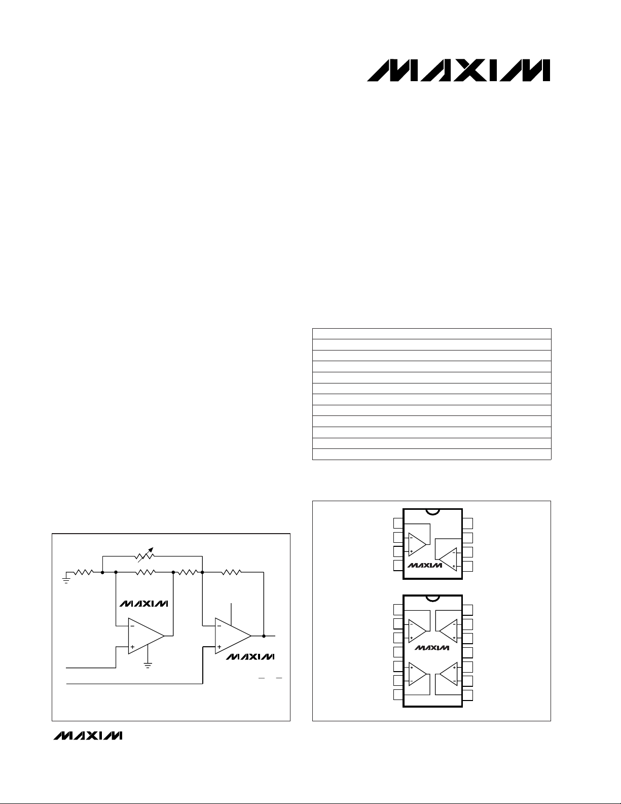
MAX478
DIP/SO
TOP VIEW
1
2
3
4
14
13
12
11
OUTD
INDIND+
V-
V+
INA+
INA-
OUTA
MAX479
DIP/SO
5
6
7
10
9
8
INC+
INCOUTC
OUTB
INB-
INB+
A
D
B
C
A
B
_________________Pin Configurations
V2
V1
R3
R1
R2 R2
R1
+5V
V
OUT
MICROPOWER, HIGH INPUT IMPEDANCE DIFFERENTIAL
AMPLIFIER WITH VARIABLE GAIN IN 8-PIN DIP/SO
1/2MAX478
1/2MAX478
V
OUT
= (V1-V2) (1 +
R1
+ 2
R1)
R2 R3
__________Typical Operating Circuit
19-0127; Rev. 1; 11/98
_______________General Description
The MAX478 and MAX479 are dual and quad micropower, precision op amps available in 8-pin and 14-pin
DIP and small-outline packages, respectively. Both
devices feature an extremely low, 17µA max supply
current per op amp, 70µV max offset voltage, 2.2µV/°C
max offset voltage drift (0.5µV/°C typ), and 250pA max
input offset current.
The MAX478 and MAX479 operate from a single supply. The input voltage range includes ground, and the
output swings to within a few millivolts of ground, which
eliminates pull-down resistors and saves power.
Both devices are optimized for single 3V and 5V supply operation, with guaranteed specifications at each
supply voltage. Specifications for ±15V operation are
also provided.
_______________________Applications
Battery- or Solar-Powered Systems:
Portable Instrumentation
Remote Sensor Amplifier
Satellite Circuitry
Micropower Sample-and-Hold
Thermocouple Amplifier
Micropower Filters
Single Lithium Cell Powered Systems
___________________________Features
♦ 17µA Max Supply Current (MAX478A/MAX479A)
♦ 70µV Max Offset Voltage (MAX478A)
♦ Single-Supply Operation:
Input Voltage Range Includes Ground
Output Swings to Ground While Sinking Current
No Pull-Down Resistors Required
♦ Dual Op Amp in 8-Pin DIP/SO Package (MAX478)
Quad Op Amp in 14-Pin DIP/SO Package (MAX479)
♦ 250pA Max Input Offset Current
(MAX478A/MAX479A)
♦ 0.5µV/°C Offset-Voltage Drift
♦ Output Sources and Sinks 5mA Load Current
______________Ordering Information
PART TEMP. RANGE PIN-PACKAGE
MAX478ACPA
0°C to+70°C 8 Plastic DIP
MAX478CPA 0°C to+70°C 8 Plastic DIP
MAX478CSA 0°C to+70°C 8 SO
MAX478C/D 0°C to+70°C Dice*
MAX478EPA -40°C to+85°C 8 Plastic DIP
MAX478ESA -40°C to+85°C 8 SO
MAX479ACPD
0°C to+70°C 14 Plastic DIP
MAX479CPD 0°C to+70°C 14 Plastic DIP
MAX479CSD 0°C to+70°C 14 SO
MAX479EPD -40°C to+85°C 14 Plastic DIP
MAX479ESD -40°C to+85°C 14 SO
* Dice are specified at TA= +25°C, DC parameters only.
MAX478/MAX479
17µA Max, Dual/Quad, Single-Supply,
Precision Op Amps
2 _______________________________________________________________________________________
Supply Voltage .............................................. ±22V
Differential Input Voltage....................................±30V
Input Voltage...................Equal to Positive Supply Voltage
...............................5V Below Negative Supply Voltage
Output Short-Circuit Duration.........................Continuous
Continuous Power Dissipation (T
A
= +70°C):
8-Pin Plastic DIP (derate 9.09mW/°C above +70°C).. ...727mW
14-Pin Plastic DIP (derate 10.00mW/°C above +70°C) .. 800mW
14-Pin Wide SO (derate 9.52mW/°C above +70°C) ...762mW
Operating Temperature Ranges:
MAX47_ACP_/C_ _...............................0°C to +70°C
MAX47_E_ _....................................-40°C to +85°C
Storage Temperature Range ...................-65°C to +150°C
Lead Temperature (soldering, 10sec)....................+300°C
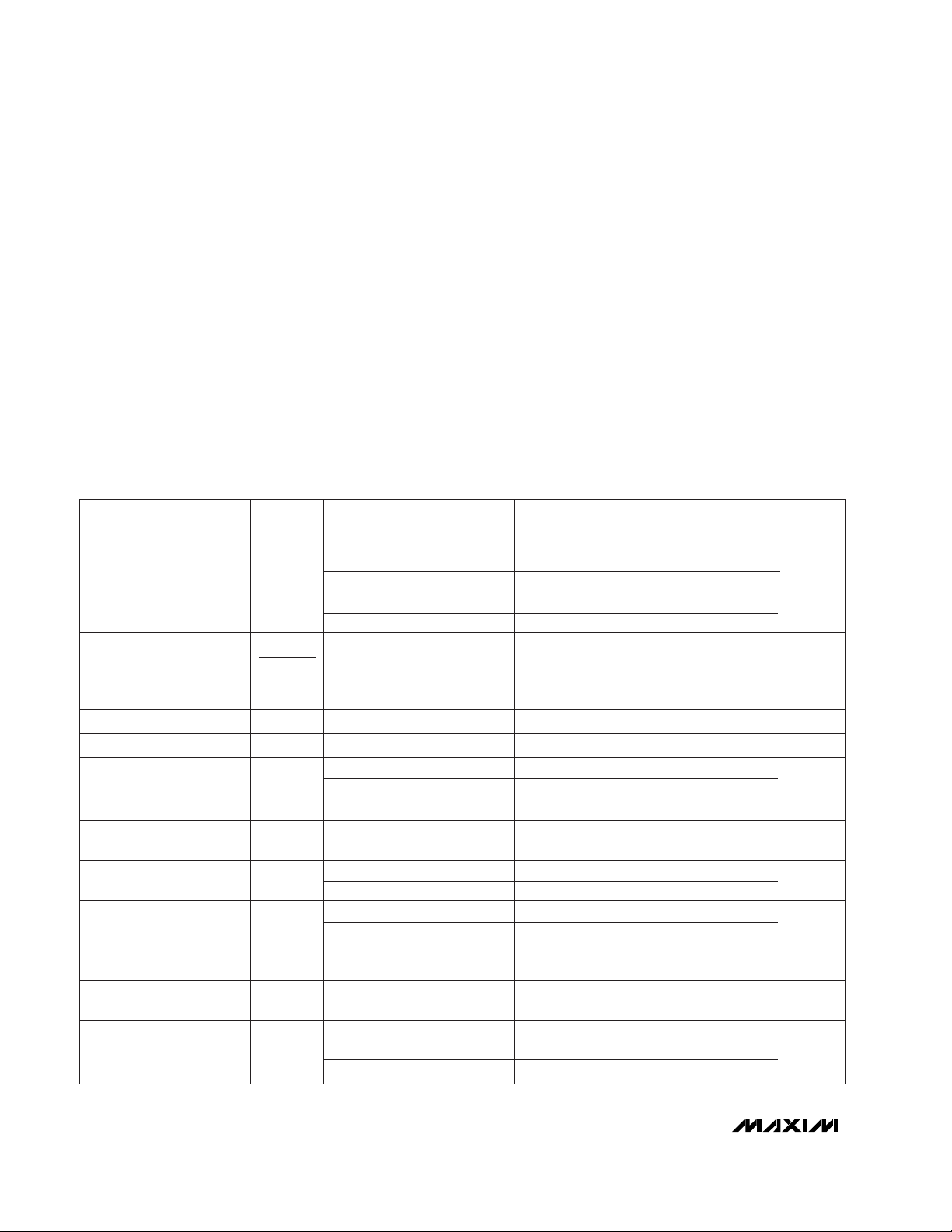
ELECTRICAL CHARACTERISTICS: 5V
(VS= 5V, 0V, VCM= 0.1V, VO= 1.4V, TA= +25°C, unless otherwise noted.)
Stresses beyond those listed under “Absolute Maximum Ratings" may cause permanent damage to the device. These are stress ratings only, and functional
operation of the device at these or any other conditions beyond those indicated in the operational sections of the specifications is not implied. Exposure to
absolute maximum rating conditions for extended periods may affect device reliability.
ABSOLUTE MAXIMUM RATINGS
PARAMETER SYMBOL CONDITIONS
MAX478C/E
MAX479C/E
MIN TYP MAX
UNITS
Input Offset Voltage
V
OS
MAX478ACP/CP/EP 30 70 40 120
µV
MAX479ACP/CP/EP 35 100 40 150
MAX478CS/ES 80 180
MAX479CS/ES 90 250
∆V
OS
∆Time
0.5 0.6 µV/Mo.
I
OS
0.05 0.25 0.05 0.35 nA
Input Bias Current
I
B
35 36 nA
Input Noise Voltage
e
n
0.1Hz to 10Hz (Note 1) 0.9 2.0 0.9
µV
p-p
Input Noise Voltage
Density
fo= 10Hz (Note 1) 50 75 50
nV/√Hz
fo= 1000Hz (Note 1) 49 65 49
Input Noise Current
i
n
0.1Hz to 10Hz (Note 1) 1.5 2.5 1.5
pA
p-p
Input Noise Current
Density
fo= 10Hz (Note 1) 0.03
pA/√Hz
fo= 1000Hz 0.01 0.01
Input Resistance
R
IN
Differential mode (Note 1) 0.8 2.0 0.6 2.0
GΩ
Common mode 12 12
Input Voltage Range
V
IN (CM)
Upper limit 3.5 3.9 3.5 3.9
V
Lower limit 0 -0.3 0 -0.3
CMRR
V
CM
= 0V to 3.5V
93 103 90 102 dB
Power-Supply
Rejection Ratio
PSRR
V
S
= 2.2V to 12V
94 104 92 104 dB
Large-Signal Voltage Gain
A
VOL
140 700 110 700
V/mV
V
O
= 0.03V to 3.5V, RL= 50kΩ
80 200 70 200
MAX478AC
MAX479AC
MIN TYP MAX
Long-Term Input OffsetVoltage Stability
Input Offset Current
Common-Mode
Rejection Ratio
V
O
= 0.03V to 4V, no load
(Note 1)
0.03 0.07
MAX478/MAX479
17µA Max, Dual/Quad, Single-Supply,
Precision Op Amps
_______________________________________________________________________________________ 3
PARAMETER SYMBOL CONDITIONS
MAX478AC
MAX479AC
MIN TYP MAX
MAX478C/E
MAX479C/E
MIN TYP MAX
UNITS
Output Voltage Swing
V
OUT
Output low, no load 6.5 9.0 6.5 9.0
mVOutput low, 2kΩ to GND 0.2 0.6 0.2 0.6
Output low, I
SINK
= 100µA
120 160 120 160
4.2 4.4
V
Output high, 2kΩ to GND 3.5 3.8 3.5 3.8
Slew Rate SR
A
V
= +1, CL= 1pF (Note 1)
0.013 0.025 0.013 0.025 V/µs
Gain-Bandwidth Product GBW
f
O
≤ 5kHz
60 60 kHz
Channel Separation
∆V
IN
= 3V, RL= 10kΩ
130 130 dB
Minimum Supply Voltage V
S
(Note 2) 2.0 2.2 2.0 2.2 V
I
S
13 18 14 21
µA
Supply Current per
Amplifier
V
S
= ±1.5V, VO= 0V
12 17 13 20
Output high, no load
ELECTRICAL CHARACTERISTICS: 5V (continued)
(VS= 5V, 0V, VCM= 0.1V, VO= 1.4V, TA= +25°C, unless otherwise noted.)
4.2 4.4
ELECTRICAL CHARACTERISTICS: 5V
(VS= 5V, 0V, VCM= 0.1V, VO= 1.4V, TA= 0°C to +70°C, unless otherwise noted.)
PARAMETER SYMBOL CONDITIONS
MAX478AC
MAX479AC
MIN TYP MAX
MAX478C
MAX479C
MIN TYP MAX
UNITS
MAX479CS 130 400
Input Offset Voltage
V
OS
MAX478ACP/CP 50 170 65 250
µV
MAX479ACP/CP 60 200 70 290
MAX478CS 120 300
Input Offset Voltage Drift
∆V
OS
∆T
MAX47_ACP/CP (Note 1) 0.5 2.2 0.6 3.0
µV/°C
MAX47_CS (Note 1) 0.8 4.5
Input Offset Current
I
OS
0.06 0.35 0.06 0.50 nA
Input Bias Current
I
B
36 37 nA
CMRR
V
CM
= 0V to 3.4V
90 101 86 100 dB
Power-Supply
Rejection Ratio
PSRR
V
S
= 2.5V to 12V
90 102 88 102 dB
Large-Signal
Voltage Gain
A
VOL
105 500 80 500
V/mV
55 160 45 160
Output Voltage Swing
V
OUT
Output low, no load 8 11 8 11
mV
Output low, I
SINK
= 100µA
140 190 140 190
Output high, no load 4.1 4.3 4.1 4.3
V
Output high, 2kΩ to GND 3.3 3.8 3.3 3.8
Supply Current per Amplifier
I
S
14 21 15 24 µA
Common-Mode
Rejection Ratio
V
O
= 0.05V to 4V, no load (Note 1)
V
O
= 0.05V to 3.5V, RL= 50kΩ
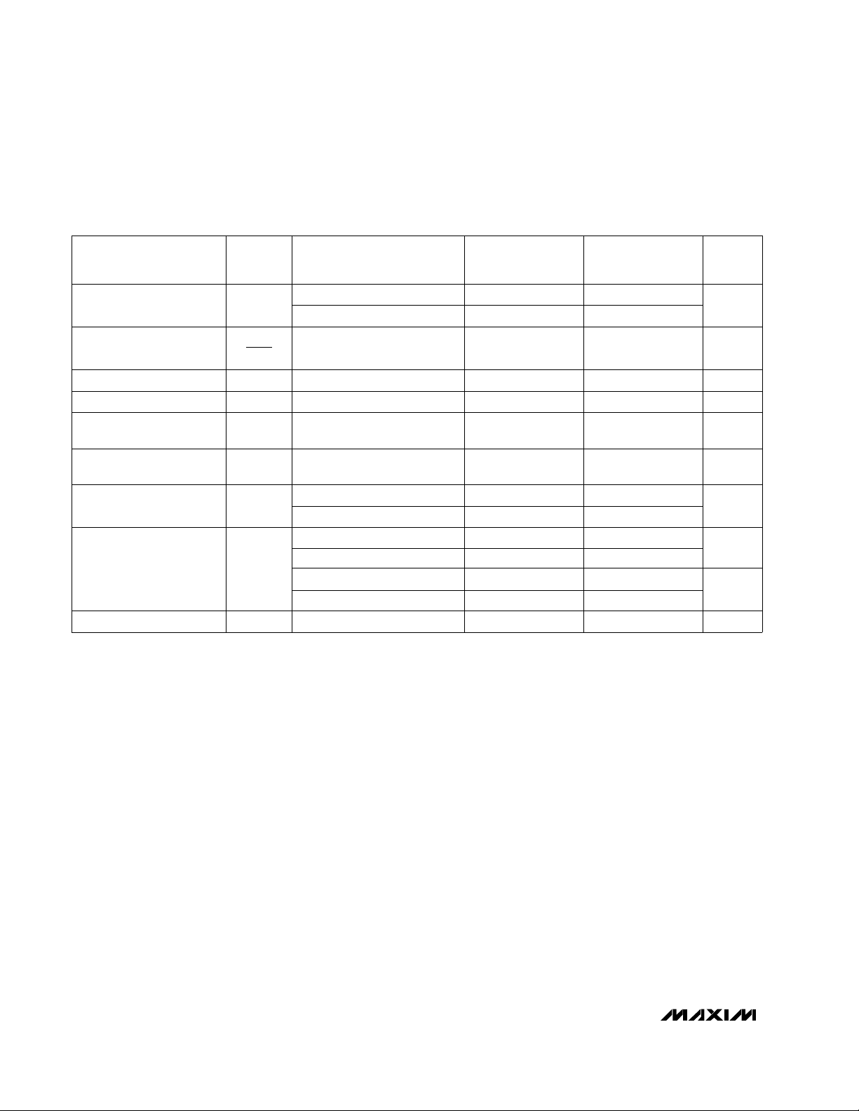
MAX478/MAX479
17µA Max, Dual/Quad, Single-Supply,
Precision Op Amps
4 _______________________________________________________________________________________
ELECTRICAL CHARACTERISTICS: 5V
(VS= 5V, 0V, VCM= 0.1V, VO= 1.4V, TA= -40°C to +85°C, unless otherwise noted.)
PARAMETER SYMBOL CONDITIONS
MAX478EP
MAX479EP
MIN TYP MAX
MAX478ES
MAX479ES
MIN TYP MAX
UNITS
Input Offset Voltage Drift
∆V
OS
∆T
(Note 1) 0.6 3.0
0.8 4.5
µV/°C
Input Offset Current
I
OS
0.07 0.7 0.07 0.7 nA
Input Bias Current
I
B
48 48 nA
Common-Mode
Rejection Ratio
CMRR
V
CM
= 0.05V to 3.2V
84 98 84 98 dB
Input Offset Voltage
V
OS
MAX478 80 315 150 400
µV
Power-Supply
Rejection Ratio
PSRR
V
S
= 3.0V to 12V
86 100 86 100 dB
Large-Signal
Voltage Gain
A
VOL
VO= 0.05V to 4V, no load (Note 1)
55 350 55 350
V/mV
MAX479 80 345 160 530
V
O
= 0.05V to 3.5V, RL= 50kΩ
35 130 35 130
Output Voltage Swing
V
OUT
Output low, no load 9 13 9 13
mV
Output low, I
SINK
= 100µA
160 220 160 220
Output high, no load 3.9 4.2 3.9 4.2
V
Output high, 2kΩ to GND 3.0 3.7 3.0 3.7
Supply Current per Amplifier
I
S
15 27 15 27 µA

MAX478/MAX479
17µA Max, Dual/Quad, Single-Supply,
Precision Op Amps
_______________________________________________________________________________________ 5
ELECTRICAL CHARACTERISTICS: 3V
(VS= 3V, 0V, VCM= 0.1V, VO= 0.8V, TA= +25°C, unless otherwise noted.)
PARAMETER SYMBOL CONDITIONS
MAX478AC
MAX479AC
MIN TYP MAX
MAX478C/E
MAX479C/E
MIN TYP MAX
UNITS
MAX479CS/ES
Input Offset Current
I
OS
90 270
0.05 0.05 nA
Input Bias Current
I
B
33nA
Common-Mode
Rejection Ratio
CMRR
V
CM
= 0V to 1.7V
93 103 90 102 dB
Input Offset Voltage
V
OS
MAX478ACP/CP/EP 30 90 40 140
µV
MAX479ACP/CP/EP 35 120 40 170
Power-Supply
Rejection Ratio
PSRR
V
S
= 2.2V to 12V
94 104 92 104 dB
Large-Signal
Voltage Gain
A
VOL
100 600 100 600
V/mV
MAX478CS/ES 80 200
V
O
= 0.03V to 1.5V, RL= 50kΩ
30 180 30 180
Output Voltage Swing
V
OUT
Output low, no load 6 9 6 9
mV
Output low, 2kΩ to GND 0.2 0.6 0.2 0.6
Output high, no load 2.2 2.4 2.2 2.4
V
Output high, 2kΩ to GND 1.8 2.0 1.8 2.0
Supply Current per Amplifier
I
S
12 17 13 20 µA
Input Noise Voltage
e
N
0.1Hz to 10Hz 1.0 1.0
µV
p-p
Input Voltage Range
V
IN (CM)
Upper limit 1.7 1.9 1.7 1.9
V
Lower limit 0 -0.3
Gain-Bandwidth Product GBW
f
O
≤ 5kHz
50 50 kHz
Minimum Supply Voltage
V
S
2.2 2.2
V
V
O
= 0.03V to 2V, no load
(Note 1)
0 -0.3
With 300µV V
OS
degradation
1.7 1.7

MAX478/MAX479
17µA Max, Dual/Quad, Single-Supply,
Precision Op Amps
6 _______________________________________________________________________________________
ELECTRICAL CHARACTERISTICS: ±15V
(VS= ±15V, TA= +25°C, unless otherwise noted.)
PARAMETER
SYMBOL CONDITIONS
MAX478AC
MAX479AC
MIN TYP MAX
MAX478C/E
MAX479C/E
MIN TYP MAX
UNITS
Input Voltage Range
V
IN (CM)
Upper limit 13.5 13.9 13.5 13.9
V
Lower limit -15.0 -15.3
Input Offset Current
I
OS
-15.0 -15.3
0.05 0.25 0.05 0.35 nA
Input Bias Current
I
B
35 36 nA
Common-Mode
Rejection Ratio
CMRR
VCM= +13.5V, -15V
97 106 94 106 dB
Slew Rate SR
AV= +1V, CL= 15pF
Power-Supply
Rejection Ratio
PSRR
VS= 5V, 0V to ±15V
96 112 94 112 dB
0.02 0.04 0.02 0.04 V/µs
16 21 17 25
Gain-Bandwidth Product GBW
fO≤ 5kHz
85 85 kHz
Input Offset Voltage
V
OS
80 350 100 480 µV
I
S
Supply Current per Amplifer µA
Large-Signal
Voltage Gain
A
VOL
VO= ±10V, RL= 50kΩ
300 1200 250 1000
V/mV
VO= ±10V, no load
600 2500 400 2500
Output Voltage Swing
V
OUT
RL= 50kΩ
±13.0 ±14.2 ±13.0 ±14.2
V
RL= 2kΩ
±11.0 ±12.7 ±11.0 ±12.7

MAX478/MAX479
17µA Max, Dual/Quad, Single-Supply,
Precision Op Amps
_______________________________________________________________________________________ 7
ELECTRICAL CHARACTERISTICS: ±15V
(VS= ±15V, TA= 0°C to +70°C, unless otherwise noted.)
PARAMETER
SYMBOL CONDITIONS
MAX478AC
MAX479AC
MIN TYP MAX
MAX478C
MAX479C
MIN TYP MAX
UNITS
I
S
Supply Current per Amplifer
MAX47_ACP/CP (Note 1) 0.6 2.8 0.7 4.0
Input Offset-Voltage Drift
∆V
OS
∆T
MAX47_CS (Note 1) 0.9 5.5
µV/°C
Large-Signal
Voltage Gain
A
VOL
VO= ±10V, RL= 50kΩ
200 800 150 750 V/mV
µA
Power-Supply
Rejection Ratio
PSRR
VS= 5V, 0V to ±15V
93 110 91 110 dB
Input Offset Voltage
V
OS
100 480 130 660
17 24 18 28
µV
Input Bias Current
I
B
36 37 nA
Common-Mode
Rejection Ratio
CMRR
VCM= +13V, -15V
94 104 91 104 dB
Output Voltage Swing
V
OUT
RL= 5kΩ
±11.0 ±13.5 ±11.0 ±13.5 V
Input Offset Current
I
OS
0.06 0.35 0.06 0.35 nA

MAX478/MAX479
17µA Max, Dual/Quad, Single-Supply,
Precision Op Amps
8 _______________________________________________________________________________________
ELECTRICAL CHARACTERISTICS: ±15V
(VS= ±15V, TA= -40°C to +85°C, unless otherwise noted.)
Note 1: Guaranteed by design.
Note 2: Power-supply rejection ratio is measured at the minimum supply voltage. The op amps actually work at 1.7V supply, but
with additional input offset-voltage skew.
PARAMETER SYMBOL CONDITIONS
MAX478EP
MAX479EP
MIN TYP MAX
MAX478ES
MAX479ES
MIN TYP MAX
UNITS
Output Voltage Swing
V
OUT
RL= 5kΩ
±11.0 ±13.5 ±11.0 ±13.5 V
Common-Mode
Rejection Ratio
CMRR
V
CM
= +13V, -14.9V
88 103 88 103 dB
I
S
Supply Current per Amplifer
Input Offset Current
I
OS
(Note 1) 0.7 4.0 0.9 5.5Input Offset-Voltage Drift
∆V
OS
∆T
µV/°C
Large-Signal
Voltage Gain
A
VOL
VO= ±10V, RL= 50kΩ
100 500 100 500 V/mV
Input Bias Current
µA
0.07 0.70 0.07 0.70 nA
I
B
Power-Supply
Rejection Ratio
PSRR
V
S
= 5V, 0V to ±15V
88 109 88 109 dB
Input Offset Voltage
V
OS
48 48 nA
130 740 130 740
19 30 19 30
µV

MAX478/MAX479
17µA Max, Dual/Quad, Single-Supply,
Precision Op Amps
_________________________________________________________________________________________________
9
__________________________________________Typical Operating Characteristics
20
-50 75
SUPPLY CURRENT
vs. TEMPERATURE
14
TEMPERATURE (°C)
SUPPLY CURRENT PER AMPLIFIER (µA)
16
-25 25
18
500
VS = ±15V
VS = 5V, 0V
VS = ±1.5V
12
10
100
100
-500
0
MINIMUM SUPPLY VOLTAGE
-400
0
POSITIVE SUPPLY VOLTAGE (V)
OFFSET-VOLTAGE SHIFT (µV)
3
-200
-300
12
-100
+25°C
+85°C
-40°C
NON-FUNCTIONAL
140
-20
0.001 100k
VOLTAGE GAIN
vs. FREQUENCY
20
FREQUENCY (Hz)
VOLTAGE GAIN (dB)
1k
60
0.1 10
100
TA = +25°C
VS = ±15V
VS = 5V, 0V
120
80
40
0
30
10k
GAIN, PHASE
vs. FREQUENCY
20
FREQUENCY (Hz)
VOLTAGE GAIN (dB)
0
-10
100k 1M
10
TA = +25°C
PHASE SHIFT (DEGREES)
80
120
200
240
160
PHASE ±15V
PHASE 5V, 0V
GAIN ±15V
GAIN 5V, 0V
120
1 100k
COMMON-MODE REJECTION RATIO
vs. FREQUENCY
0
FREQUENCY (Hz)
CMRR (dB)
40
10 1k
80
TA = +25°C
VS = 5V, 0V
10k
100
VS = ±15V
120
0.1 100k
POWER-SUPPLY REJECTION RATIO
vs. FREQUENCY
0
FREQUENCY (Hz)
PSRR (dB)
40
11k
80
10k
100
POSITIVE SUPPLY
NEGATIVE SUPPLY
VS = ±2.5V + 1V
p-p
SINE WAVE
T
A
= +25°C
10
120
0
100
40
CAPACITIVE LOAD (pF)
OVERSHOOT (%)
100010
80
10,000
CAPACITIVE LOAD HANDLING
VS = 5V, 0V
T
A
= +25°C
AV = +1
AV = +5
AV = +10
100
60
20
1000
0.1
0
OUTPUT SATURATION
vs. TEMPERATURE
10
TEMPERATURE (°C)
SATURATION VOLTAGE (mV)
50-50
100
100
1
I
SINK
= 1mA
I
SINK
= 100µA
I
SINK
= 1µA
NO LOAD
2kΩ TO GROUND
VS = 5V, 0V
-25 25 75
10kΩ TO GROUND
10M
10k
100k
VOLTAGE GAIN
vs. LOAD RESISTANCE
100k
LOAD RESISTANCE TO GROUND (Ω)
VOLTAGE GAIN (V/V)
1M10k
1M
10M
VS = ±15V, TA = +25°C
VS = 5V, 0V,
T
A
= +25°C
VS = 5V, 0V,
T
A
= +85°C

MAX478/MAX479
17µA Max, Dual/Quad, Single-Supply,
Precision Op Amps
10
_______________________________________________________________________________________________
1000
10
0.1 1 1k
NOISE SPECTRUM
100
FREQUENCY (Hz)
VOLTAGE NOISE DENSITY (nV/√
Hz
)
CURRENT NOISE DENSITY (fA/√
Hz
)
30
300
10 100
CURRENT NOISE
1/f CORNER
0.5Hz
VOLTAGE NOISE
VS = ±2.5V
T
A
= +25°C
20
-30
0
SHORT-CIRCUIT CURRENT
10
TIME FROM OUTPUT SHORT TO GROUND (MINUTES)
SHORT-CIRCUIT CURRENT (mA)
-10
-20
1
0
SINKING SOURCING
2
VS = 5V, 0V
VS = ±15V
VS = ±2.5V
VS = ±2.5V
VS = ±15V
100
-4.0
-50
INPUT BIAS AND OFFSET CURRENT
vs. TEMPERATURE
TEMPERATURE (°C)
INPUT BIAS
CURRENT (nA)
100
-2.5
-25 0
50
75
25
-3.0
-3.5
25
50
75
INPUT OFFSET
CURRENT (pA)
VS = 5V, 0V
I
OS
I
B
____________________________Typical Operating Characteristics (continued)
LARGE-SIGNAL TRANSIENT RESPONSE
VS= ±15V
TIME (500µs/div)
AV= +1, CL= 15pF
LARGE-SIGNAL TRANSIENT RESPONSE
VS= 5V, 0V
TIME (100µs/div)
AV= +1, CL= 15pF
SMALL-SIGNAL TRANSIENT RESPONSE
VS= ±2.5V
TIME (20µs/div)
AV= +1, CL= 15pF
SMALL-SIGNAL TRANSIENT RESPONSE
VS= ±15V
TIME (20µs/div)
AV= +1, CL= 15pF
SMALL-SIGNAL TRANSIENT RESPONSE
VS= 5V, 0V
TIME (20µs/div)
AV= +1, CL= 15pF
OUTPUT VOLTAGE (20mV/div)
OUTPUT VOLTAGE (20mV/div)
OUTPUT VOLTAGE (20mV/div)
OUTPUT VOLTAGE (1V/div)
100mV
OUTPUT VOLTAGE (5V/div)
0V
2V
0V
0V

________________________________________________________Package Information
MAX478/MAX479
17µA Max, Dual/Quad, Single-Supply,
Precision Op Amps
______________________________________________________________________________________ 11
IN+
IN-
R1
OUTPUT
LOW-POWER INSTRUMENTATION AMPLIFIER
1/4MAX479
1/4MAX479
GAIN = (1 +
2R1) (R3)
= 100 FOR VALUES SHOWN
RG R2
1/4MAX479
1M
RG
200k
R1
1M
R2
1M
R3
9.1M
R3
9.1M
R2
1M
________Typical Application Circuit ___________________Chip Topograqhy
OUTA
V+
0.111"
(2.82mm)
V- V+
OUTB
INA-
INA+
INB-
INB+
0.079"
(2.01mm)
SOICN.EPS

MAX478/MAX479
17µA Max, Dual/Quad, Single-Supply,
Precision Op Amps
Maxim cannot assume responsibility for use of any circuitry other than circuitry entirely embodied in a Maxim product. No circuit patent licenses are
implied. Maxim reserves the right to change the circuitry and specifications without notice at any time.
12
____________________Maxim Integrated Products, 120 San Gabriel Drive, Sunnyvale, CA 94086 408-737-7600
© 1998 Maxim Integrated Products Printed USA is a registered trademark of Maxim Integrated Products.
__________________________________________Package Information (continued)
PDIPN.EPS
 Loading...