

General Description
The MAX4789–MAX4794 family of switches feature
internal current limiting to prevent damage to host
devices due to faulty load conditions. These analog
switches have a low 0.2Ω on-resistance and operate
from 2.3V to 5.5V input voltage range. They are available with guaranteed 200mA, 250mA, and 300mA current limits, making them ideal for SDIO and other load
switching applications.
When the switch is on and a load is connected to the
port, a guaranteed blanking time of 14ms ensures that
the transient voltages settle down. If after this blanking
time the load current is greater than the current limit,
the MAX4789, MAX4791, and MAX4793 enter a latchoff state where the switch is turned off and FLAG is
issued to the microprocessor. The switch can be turned
on again by cycling the power or the ON pin.
The MAX4790, MAX4792, and MAX4794 have an
autoretry feature where the switch turns off after the
blanking time and then continuously checks to see if
the overload condition is present. The switch remains
on after the overload condition disappears.
The MAX4789–MAX4794 are available in 6-pin thin QFN
and tiny space-saving 4-pin SOT143 packages. The
MAX4789/MAX4791/MAX4793 are also available in a
tiny 5-pin SOT23 package. For lower current current-limiting switches, refer to the MAX4785–MAX4788 data sheet.
Applications
PDAs and Palmtop Devices
Cell Phones
GPS Systems
Hand-Held Devices
SDIO
Features
♦ Guaranteed Current Limit: 200mA, 250mA, 300mA
♦ Thermal-Shutdown Protection
♦ Reverse Current Protection
♦ 0.2Ω On-Resistance
♦ 14ms Guaranteed Blanking Time
♦ FLAG Function (MAX4789/MAX4791/MAX4793)
♦ 80µA Supply Current
♦ 8µA Latch-Off Current
(MAX4789/MAX4791/MAX4793)
♦ 0.01µA Shutdown Current
♦ 2.3V to 5.5V Supply Range
♦ Undervoltage Lockout
♦ Fast Current-Limit Response Time (5µs)
♦ Tiny QFN and SOT23/SOT143 Packages
MAX4789–MAX4794
200mA/250mA/300mA Current-Limit Switches
________________________________________________________________ Maxim Integrated Products 1
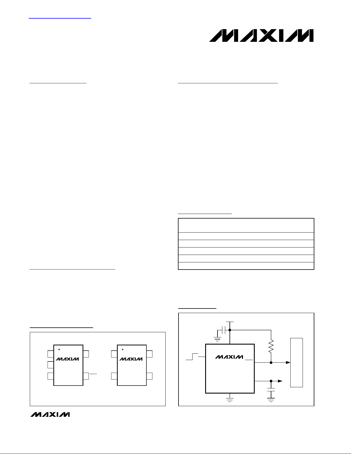
Ordering Information
2.3V TO 5.5V
IN
OUT
FLAG
GND
ON
µP
TO SDIO PORT
MAX4789
MAX4791
MAX4793
Typical Operating Circuit
19-2663; Rev 1; 8/03
For pricing, delivery, and ordering information, please contact Maxim/Dallas Direct! at
1-888-629-4642, or visit Maxim’s website at www.maxim-ic.com.
*EP = Exposed pad.
Ordering Information continued at end of data sheet.
Selector Guide appears at end of data sheet.
Pin Configurations
查询MAX4789供应商查询MAX4789供应商
PART TEMP RANGE PIN-PACKAGE
MAX4789EUS-T -40°C to +85°C 4 SOT143-4 KAFE
MAX4789EUK-T -40°C to +85°C 5 SOT23-5 AEAC
MAX4789ETT -40°C to +85°C 3 x 3 Thin QFN-EP* ABO
MAX4790EUS-T -40°C to +85°C 4 SOT143-4 KAFF
MAX4790ETT -40°C to +85°C 3 x 3 Thin QFN-EP ABP
TOP
MARK
TOP VIEW
15OUTIN
MAX4789
2
GND
ON ON
Pin Configurations continued at end of data sheet.
MAX4791
MAX4793
34
SOT23
FLAG
14INOUT
MAX4789–
MAX4794
23GND
SOT143
MAX4789–MAX4794
200mA/250mA/300mA Current-Limit Switches
2 _______________________________________________________________________________________
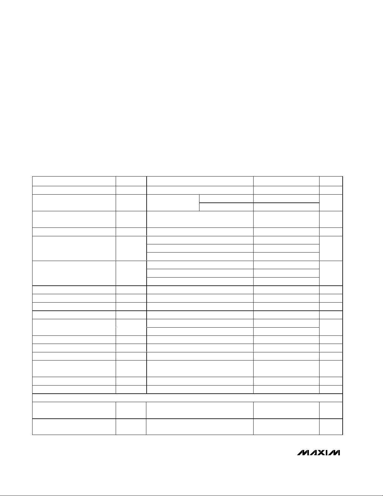
ABSOLUTE MAXIMUM RATINGS
ELECTRICAL CHARACTERISTICS
(VIN= 2.3V to 5.5V, TA= -40°C to +85°C, unless otherwise noted. Typical values are at VIN= 3.3V, TA= +25°C.) (Note 1)
Stresses beyond those listed under “Absolute Maximum Ratings” may cause permanent damage to the device. These are stress ratings only, and functional
operation of the device at these or any other conditions beyond those indicated in the operational sections of the specifications is not implied. Exposure to
absolute maximum rating conditions for extended periods may affect device reliability.
IN, ON, FLAG, OUT to GND .....................................-0.3V to +6V
OUT Short Circuit to GND .................................Internally Limited
Continuous Power Dissipation (T
A
= +70°C)
4-Pin SOT143 (derate 4.0mW/°C above +70°C)..........320mW
5-Pin SOT23 (derate 7.1mW/°C above +70°C)............571mW
6-Pin Thin QFN (derate 24.4mW/°C above +70°C)...1951.2mW
Operating Temperature Range ...........................-40°C to +85°C
Junction Temperature......................................................+150°C
Storage Temperature Range .............................-65°C to +150°C
Lead Temperature (soldering, 10s) .................................+300°C
Operating Voltage V
Quiescent Current I
Latch-Off Current (Note 2) I
Shutdown Current I
Reverse Current Limit
ON Input Leakage VON = VIN or GND -1 +1 µA
Off Switch Leakage VON = 0V, V
Undervoltage Lockout UVLO Rising edge 1.8 2.2 V
Undervoltage Lockout Hysteresis 100 mV
On-Resistance R
ON Input Logic High Voltage V
ON Input Logic Low Voltage V
FLAG Output Logic Low Voltage I
FLAG Output High Leakage
Current
Thermal Shutdown 150 °C
Thermal-Shutdown Hysteresis 15 °C
DYNAMIC
Turn-On Time (Note 3)
Turn-Off Time (Note 3)
PARAMETER SYMBOL CONDITIONS MIN TYP MAX UNITS
IN
VON = VIN, I
Q
switch on
LATCH
SHDN
ON
VON = VIN, after an overcurrent fault
(MAX4789/MAX4791/MAX4793)
VON = 0V 0.01 1 µA
MAX4789/MAX4790 200 300
MAX4791/MAX4792 250 375Forward Current Limit
MAX4793/MAX4794 300 450
MAX4789/MAX4790 300
MAX4791/MAX4792 375
MAX4793/MAX4794 450
TA = +25°C, I
TA = - 40° C to + 85°C , I
IH
IL
= 1m A ( M AX 4789/M AX 4791/M AX 4793) 0.4 V
S IN K
VIN = V
FLAG
(MAX4789/MAX4791/MAX4793)
V
from low to high; I
ON
C
= 0.1µF
L
V
from high to low; I
ON
C
= 0.1µF
L
2.3 5.5 V
VIN = +2.3V to +5.0V 80 120
= 0,
OUT
= +5.0V to +5.5V 160
V
IN
815µA
= 0V 0.01 1 µA
OUT
= 100mA 0.2 0.4
OUT
= 100m A 0.5
OU T
2.0 V
0.8 V
= 5.5V
OUT
OUT
= 10mA,
= 10mA,
100 µs
40 ns
1µA
µA
mA
mA
Ω
MAX4789–MAX4794
200mA/250mA/300mA Current-Limit Switches
_______________________________________________________________________________________ 3
Typical Operating Characteristics
(VIN= 3.3V, TA= +25°C, unless otherwise noted.)
Note 1: All parts are 100% tested at +25°C. Limits across the full temperature range are guaranteed by design and correlation.
Note 2: Latch-off current does not include the current flowing into FLAG.
Note 3: The on time is defined as the time taken for the current through the switch to go from 0mA to full load. The off-time is defined
as the time taken for the current through the switch to go from full load to 0mA.
Note 4: Retry time is typically 7 times the blanking time.
ELECTRICAL CHARACTERISTICS (continued)
(VIN= 2.3V to 5.5V, TA= -40°C to +85°C, unless otherwise noted. Typical values are at VIN= 3.3V, TA= +25°C.) (Note 1)
Blanking Time t
Short-Circuit Current-Limit
Response Time
Retry Time (Note 4) t
PARAMETER SYMBOL CONDITIONS MIN TYP MAX UNITS
BLANK
RETRY
Overcurrent fault (Figures 2, 3) 14 60 ms
VON = VIN = 3.3V, short circuit applied to
OUT
5µs
MAX4790/MAX4792/MAX4794 (Figure 2) 98 420 ms
QUIESCENT SUPPLY CURRENT
vs. SUPPLY VOLTAGE
100
VON = VIN
90
80
70
60
50
40
30
SUPPLY CURRENT (µA)
20
10
0
2.0
SUPPLY VOLTAGE (V)
MAX4789 toc01
5.55.04.0 4.53.0 3.52.5
120
100
80
60
40
SUPPLY CURRENT (µA)
20
0
-40 85
vs. TEMPERATURE
VON = VIN
VIN = 5V
SUPPLY CURRENT
VIN = 3.3V
TEMPERATURE (°C)
LATCH-OFF CURRENT
vs. TEMPERATURE
15
VON = VIN
14
13
MAX4789 toc02
12
11
10
9
8
7
6
LATCH-OFF (µA)
5
4
3
2
1
0
603510-15
-40 85
VIN = 5V
VIN = 3.3V
603510-15
TEMPERATURE (°C)
MAX4789 toc03
SHUTDOWN SUPPLY CURRENT
vs. TEMPERATURE
100
10
1
0.1
0.01
SHUTDOWN SUPPLY CURRENT (nA)
0.001
-40 85
VCC = 5V
TEMPERATURE (°C)
VCC = 3.3V
603510-15
SHUTDOWN LEAKAGE CURRENT
10
MAX4789 toc04
1
0.1
0.01
0.001
SHUTDOWN LEAKAGE CURRENT (nA)
0.0001
-40 85
vs. TEMPERATURE
VIN = 5V
TEMPERATURE (°C)
VIN = 3.3V
603510-15
LATCH-OFF LEAKAGE CURRENT
100
10
MAX4789 toc05
1
0.1
0.01
0.001
LATCH-OFF LEAKAGE CURRENT (nA)
0.0001
VIN = 5V
-40 85
vs. TEMPERATURE
MAX4789 toc06
VIN = 3.3V
603510-15
TEMPERATURE (°C)
MAX4789–MAX4794
200mA/250mA/300mA Current-Limit Switches
4 _______________________________________________________________________________________
Typical Operating Characteristics (continued)
(VIN= 3.3V, TA= +25°C, unless otherwise noted.)
ON
NORMALIZED R
1000
NORMALIZED ON-RESISTANCE
vs. TEMPERATURE
1.4
1.2
1.0
0.8
0.6
0.4
0.2
0
-40 85
VCC = 5V
TEMPERATURE (°C)
SWITCH TURN-ON/OFF TIMES
vs. TEMPERATURE
100
ON
OUTPUT CURRENT
vs. OUTPUT VOLTAGE
500
MAX4789 toc07
603510-15
450
400
350
300
250
200
150
OUTPUT CURRENT (mA)
100
50
MAX4793/MAX4794
MAX4789/MAX4790
MAX4791/MAX4792
0
03.3
VIN - V
(V)
OUT
3.02.72.1 2.40.6 0.9 1.2 1.5 1.80.3
FLAG-BLANKING TIMEOUT
vs. TEMPERATURE
50
MAX4789 toc09
45
MAX4789 toc08
MAX4789 toc10
VCC = 5V
OFF
TURN-ON/OFF TIMES (µs)
0.001
10
0.1
0.01
VCC = 3.3V
1
-40 85
TEMPERATURE (°C)
CURRENT-LIMIT RESPONSE
VIN = 3.3V
= 1µF
C
IN
40µs/div
I
LOAD
C
= 10mA
603510-15
MAX4789 toc11
= 1µF
OUT
V
IN
2V/div
V
ON
2V/div
I
OUT
100mA/div
40
35
30
FLAG-BLANKING TIME (ms)
25
20
-40 85
TEMPERATURE (°C)
CURRENT-LIMIT RESPONSE
VIN = V
ON
CIN = 1µF
C
= 1µF
OUT
20µs/div
603510-15
MAX4789 toc12
= V
V
IN
ON
1V/div
I
OUT
100mA/div

MAX4789–MAX4794
200mA/250mA/300mA Current-Limit Switches
_______________________________________________________________________________________ 5
Pin Description
SWITCH TURN-ON TIME RESPONSE
MAX4789 toc14
100µs/div
V
ON
1V/div
I
OUT
10mA/div
CURRENT-LIMIT RESPONSE
(OUT SHORTED TO GND)
MAX4789 toc13
40µs/div
V
IN
2V/div
V
OUT
2V/div
I
OUT
5A/div
CIN = 1µF
C
OUT
= 1µF
Typical Operating Characteristics (continued)
(VIN= 3.3V, TA= +25°C, unless otherwise noted.)
SWITCH TURN-OFF TIME RESPONSE
MAX4789 toc15
V
ON
2V/div
FLAG-BLANKING RESPONSE
MAX4789 toc16
V
IN
2V/div
V
ON
2V/div
QFN
MAX4789
MAX4791
MAX4793
1 — 4 — FLAG
2 2 2 2 GND Ground
3 3 3 3 ON Active-High Switch On Input. A logic high turns the switch on.
QFN
MAX4790
MAX4792
MAX4794
4 1, 4 ——N.C. No Connection. Not internally connected.
5 5 1 4 IN Input. Bypass with a 0.1µF ceramic capacitor to ground.
6 6 5 1 OUT Switch Output. Bypass with a 0.1µF ceramic capacitor to ground.
PIN
5-SOT23
MAX4789
MAX4791
MAX4793
200ns/div
4-SOT143
MAX4789–
MAX4794
I
OUT
10mA/div
4ms/div
NAME FUNCTION
Fault Output. This open-drain output goes low when the device stays in
forward or reverse current limit for more than the blanking time period.
FLAG is high impedance when a fault is not present or when ON is low.
FLAG
2V/div
I
OUT
100mA/div

MAX4789–MAX4794
Detailed Description
The MAX4789–MAX4794 are forward/reverse currentlimited switches that operate from a 2.3V to 5.5V input
voltage range and guarantee a 200mA, 250mA, and
300mA minimum current-limit threshold for different
options. The voltage drop across an internal sense
resistor is compared to two reference voltages to indicate a forward or reverse current-limit fault. When the
load current exceeds the preset current limit for greater
than the fault-blanking time, the switch opens.
The MAX4790, MAX4792, and MAX4794 have an
autoretry function that turns on the switch again after an
internal retry time expires. If the faulty load condition is
still present after the blanking time, the switch turns off
again and the cycle is repeated. If the faulty load condition is not present, the switch remains on.
The MAX4789, MAX4791, and MAX4793 do not have
the autoretry option and the switch remains in latch-off
mode until the ON pin or the input power is cycled from
high to low and then high again.
The undervoltage lockout (UVLO) circuit prevents erroneous switch operation when the input voltage goes too
low during startup conditions.
Reverse Current Protection
The MAX4789–MAX4794 limit the reverse current (V
OUT
to VIN) from exceeding the maximum I
REV
value. The
switch is shut off and FLAG is asserted (MAX4789/
MAX4791/MAX4793) if the reverse current-limit condition
persists for more than the blanking time. This feature prevents excessive reverse currents from flowing through the
device.
Switch-On/Off Control
Toggle ON high to enable the current-limited switches.
The switches are continuously on, only if VINexceeds the
UVLO threshold (typically 2V) and there is no fault. When
a forward/reverse current fault is present or the die
exceeds the thermal-shutdown temperature of +150°C,
OUT is internally disconnected from IN and the supply
current decreases to 8µA (latch off). The switch is now
operating in one of its off states. The switch-off state also
occurs when driving ON low, thus reducing the supply
current (shutdown) to 0.01µA. Table 1 illustrates the
ON/OFF state of the MAX4789–MAX4794 current-limit
switches.
FLAG
Indicator
The MAX4789, MAX4791, and MAX4793 feature a
latched fault output, FLAG. Whenever a fault is activated, it latches FLAG output low and also turns the switch
200mA/250mA/300mA Current-Limit Switches
6 _______________________________________________________________________________________
Figure 1. Functional Diagram
IN
ON
UNDERVOLTAGE
LOGIC
LOCKOUT
+2.0V
AUTORETRY
REVERSE CURRENT
FORWARD CURRENT
N
DETECTOR
DETECTOR
BLANKING TIME
CIRCUITRY
MAX4789–MAX4794
MAX4789/MAX4791/
MAX4793 ONLY
FLAG
N
OUT
GND

off. FLAG is an open-drain output transistor and requires
an external pullup resistor from FLAG to IN. During shutdown (ON is low), the pulldown on FLAG output is
released in order to limit power dissipation. FLAG goes
low when any of the following conditions occur:
• The die temperature exceeds the thermal-shutdown
temperature limit of +150°C.
• The device is in current limit for more than the faultblanking period.
• V
IN
is below UVLO threshold.
Autoretry (MAX4790/MAX4792/MAX4794)
When the forward or reverse current-limit threshold is
exceeded, t
BLANK
timer begins counting (Figure 2).
The timer resets if the overcurrent condition disappears
before t
BLANK
has elapsed. A retry time delay, t
RETRY
,
is started immediately after t
BLANK
has elapsed and
during that time, the switch is latched off. At the end of
t
RETRY
, the switch is turned on again. If the fault still
exists, the cycle is repeated. If the fault has been
removed, the switch stays on.
The autoretry feature saves system power in the case
of an overcurrent or short-circuit condition. During
t
BLANK
, when the switch is on, the supply current is at
the current limit. During t
RETRY
, when the switch is off,
the current through the switch is zero. Instead of
observing the full load current, the switch sees the
equivalent load current times duty cycle or I
SUPPLY
=
I
LOAD
✕ t
BLANK
/(t
BLANK
+ t
RETRY
). With a typical
t
BLANK
= 37ms and typical t
RETRY
= 259ms, the duty
cycle is 12%, which results in an 88% power savings
over the switch being on the entire time. The duty cycle
is consistent across the process and devices.
Latch Off (MAX4789/MAX4791/MAX4793)
When the forward or reverse current-limit threshold is
exceeded, t
BLANK
timer begins counting. The timer
resets if the overcurrent condition disappears before
t
BLANK
has elapsed. The switch is shut off if the over-
current condition continues up to the end of the blank-
ing time. Reset the switch by either toggling ON (Figure
3a) or cycling the input voltage below UVLO, typically
2V (Figure 3b).
Fault Blanking
The MAX4789–MAX4794 feature 14ms (min) fault blanking. Fault blanking allows current-limit faults, including
momentary short-circuit faults that occur when hot
swapping a capacitive load, and also ensures that no
fault is issued during power-up. When a load transient
causes the device to enter current limit, an internal
counter starts. If the load-transient fault persists beyond
the fault-blanking timeout, the MAX4789/MAX4791/
MAX4793 FLAG asserts low. Load-transient faults less
than t
BLANK
do not cause a FLAG output assertion. Only
current-limit faults are blanked.
A thermal fault and input voltage drops below the
UVLO threshold cause FLAG to assert immediately and
do not wait for the blanking time.
Thermal Shutdown
The MAX4789–MAX4794 have a thermal shutdown feature to protect the devices from overheating. The switch
turns off and FLAG goes low immediately (no fault blank-
ing) when the junction temperature exceeds +150°C.
The switch turns back on when the device temperature
drops approximately 15°C.
MAX4789–MAX4794
200mA/250mA/300mA Current-Limit Switches
_______________________________________________________________________________________ 7
Table 1. MAX4789–MAX4794 Switch Truth Table
Figure 2. MAX4790/MAX4792/MAX4794 Autoretry Fault
Blanking Diagram
ON FAULT SWITCH ON/OFF SUPPLY CURRENT MODE
Low X OFF Shutdown
High Undervoltage Lockout OFF Shutdown
High Thermal OFF immediately (t
High Current Limit
OFF after t
ON during t
MAX4790, MAX4792, and MAX4794; cycle repeats until fault
is removed
BLANK
BLANK
period has elapsed Latch off
period does not apply) Latch off
BLANK
period, OFF during t
period for the
RETRY
t
BLANK
t
RETRY
See the Autoretry section
t
BLANK
t
BLANK
LOAD
CURRENT
ON
SWITCH
STATUS
OFF
CURRENT
LIMIT
SHORT
CONDITION
REMOVED

MAX4789–MAX4794
Applications Information
Input Capacitor
To limit the input voltage drop during momentary output
short-circuit conditions, connect a capacitor from IN to
GND. A 0.1µF ceramic capacitor is adequate for most
applications; however, higher capacitor values further
reduce the voltage drop at the input and are recommended for lower voltage applications.
Output Capacitance
Connect a 0.1µF capacitor from OUT to GND. This
capacitor helps prevent inductive parasitics from
pulling OUT negative during turn-off, thus preventing
the MAX4789–MAX4794 from tripping erroneously. If
the load capacitance is too large, then current may not
have enough time to charge the capacitance and the
device assumes that there is a faulty load condition.
The maximum capacitive load value that can be driven
from OUT is obtained by the following formula:
Layout and Thermal Dissipation
To optimize the switch response time to output shortcircuit conditions, it is very important to keep all traces
as short as possible to reduce the effect of undesirable
parasitic inductance. Place input and output capacitors
as close as possible to the device (no more than 5mm).
IN and OUT pins must be connected with short traces
to the power bus.
During normal operation, the power dissipation is small
and the package temperature change is minimal. If the
output is continuously shorted to ground at the maximum supply voltage, the operation of the switches with
the autoretry option does not cause problems because
the total power dissipated during the short is scaled by
the duty cycle:
where VIN= 5.5V, I
OUT
= 450mA, t
BLANK
= 14ms, and
t
RETRY
= 98ms.
Attention must be given to the MAX4789, MAX4791,
and MAX4793 where the latch-off condition must be
manually reset by toggling ON from high to low. If the
latch-off time duration is not sufficiently high, it is possible for the device to reach the thermal-shutdown
threshold and never be able to turn the device on until
it cools down.
Chip Information
TRANSISTOR COUNT: 1408
PROCESS: BiCMOS
200mA/250mA/300mA Current-Limit Switches
8 _______________________________________________________________________________________
Figure 3. MAX4789/MAX4791/MAX4793 Latch-Off Fault
Blanking
t
BLANK
LOAD
CURRENT
ON
SWITCH
STATUS
OFF
ON PIN
VOLTAGE
FLAG PIN
STATUS
t
BLANK
LOAD
CURRENT
ON
SWITCH
STATUS
OFF
IN PIN
VOLTAGE
FLAG PIN
STATUS
UVLO
(a)
t
BLANK
(b)
t
BLANK
C
It
FWD MIN BLANK MIN
<
MAX
×
__
V
IN
VI t
P
MAX
IN MAX OUT MAX BLANK
=
××
__
tt
+
RETRY BLANK
mW
=
302

MAX4789–MAX4794
200mA/250mA/300mA Current-Limit Switches
_______________________________________________________________________________________ 9
Selector Guide
Pin Configurations (continued) Ordering Information (continued)
TOP VIEW
FLAG (N.C.)
*( ) FOR THE MAX4790, MAX4792, AND MAX4794.
PART
MAX4789EUS 4-SOT143 200 No No
MAX4789EUK 5-SOT23 200 Yes No
MAX4789ETT 6-QFN 200 Yes No
MAX4790EUS 4-SOT143 200 No Yes
MAX4790ETT 6-QFN 200 No Yes
MAX4791EUS 4-SOT143 250 No No
MAX4791EUK 5-SOT23 250 Yes No
MAX4791ETT 6-QFN 250 Yes No
MAX4792EUS 4-SOT143 250 No Yes
MAX4792ETT 6-QFN 250 No Yes
MAX4793EUS 4-SOT143 300 No No
MAX4793EUK 5-SOT23 300 Yes No
MAX4793ETT 6-QFN 300 Yes No
MAX4794EUS 4-SOT143 300 No Yes
MAX4794ETT 6-QFN 300 No Yes
1 OUT
MAX4789–
2
GND
PACKAGE
MAX4794
3
3 x 3 THIN QFN
PIN-
C U R R EN T
L IM IT ( m A )
6
5
IN
4ON
N.C.
F L A G
F U N C T IO N
AUTO-
RETRY
PART TEMP RANGE PIN-PACKAGE
MAX4791EUS-T -40°C to +85°C 4 SOT143-4 KAFG
MAX4791EUK-T -40°C to +85°C 5 SOT23-5 AEAE
MAX4791ETT -40°C to +85°C 3 x 3 Thin QFN-EP ABQ
MAX4792EUS-T -40°C to +85°C 4 SOT143-4 KAFH
MAX4792ETT -40°C to +85°C 3 x 3 Thin QFN-EP ABR
MAX4793EUS-T -40°C to +85°C 4 SOT143-4 KAFI
MAX4793EUK-T -40°C to +85°C 5 SOT23-5 AEAG
MAX4793ETT -40°C to +85°C 3 x 3 Thin QFN-EP ABS
MAX4794EUS-T -40°C to +85°C 4 SOT143-4 KAFJ
MAX4794ETT -40°C to +85°C 3 x 3 Thin QFN-EP ABT
TOP
MARK

MAX4789–MAX4794
200mA/250mA/300mA Current-Limit Switches
10 ______________________________________________________________________________________
Package Information
(The package drawing(s) in this data sheet may not reflect the most current specifications. For the latest package outline information,
go to www.maxim-ic.com/packages.)
SOT-143 4L.EPS
PACKAGE OUTLINE, SOT-143, 4L
21-0052
E
1
1

MAX4789–MAX4794
200mA/250mA/300mA Current-Limit Switches
______________________________________________________________________________________ 11
Package Information (continued)
(The package drawing(s) in this data sheet may not reflect the most current specifications. For the latest package outline information,
go to www.maxim-ic.com/packages.)
SOT-23 5L .EPS
PACKAGE OUTLINE, SOT-23, 5L
21-0057
1
E
1

MAX4789–MAX4794
200mA/250mA/300mA Current-Limit Switches
Maxim cannot assume responsibility for use of any circuitry other than circuitry entirely embodied in a Maxim product. No circuit patent licenses are
implied. Maxim reserves the right to change the circuitry and specifications without notice at any time.
12 ____________________Maxim Integrated Products, 120 San Gabriel Drive, Sunnyvale, CA 94086 408-737-7600
© 2003 Maxim Integrated Products Printed USA is a registered trademark of Maxim Integrated Products.
Package Information (continued)
(The package drawing(s) in this data sheet may not reflect the most current specifications. For the latest package outline information,
go to www.maxim-ic.com/packages.)
L
PIN 1 ID
1N1
[(N/2)-1] x e
REF.
6, 8, &10L, QFN THIN.EPS
PIN 1
INDEX
AREA
D
E
A
A2
b
E2
DETAIL A
e
D2
C0.35
A
NUMBER OF LEADS SHOWN ARE FOR REFERENCE ONLY
COMMON DIMENSIONS
MIN. MAX.
SYMBOL
0.70 0.80
A
2.90 3.10
D
E
2.90 3.10
0.00 0.05
A1
L
0.20 0.40
k
0.25 MIN.
A2 0.20 REF.
PACKAGE VARIATIONS
PKG. CODE
T633-1 1.50–0.10D22.30–0.10
N
6
1.50–0.10
2.30–0.10T833-1 8
A1
E2
0.95 BSCeMO229 / WEEA
0.65 BSC
L
JEDEC SPEC
MO229 / WEEC
C
L
e
0.40–0.05b1.90 REF
0.25–0.05 2.00 REFMO229 / WEED-30.50 BSC1.50–0.10 2.30–0.1010T1033-1
k
C
L
e
DALLAS
SEMICONDUCTOR
PROPRIETARY INFORMATION
TITLE:
PACKAGE OUTLINE, 6, 8 & 10L,
TDFN, EXPOSED PAD, 3x3x0.80 mm
APPROVAL
[(N/2)-1] x e
1.95 REF0.30–0.05
DOCUMENT CONTROL NO. REV.
21-0137 D
L
1
2
DALLAS
SEMICONDUCTOR
PROPRIETARY INFORMATION
TITLE:
PACKAGE OUTLINE, 6, 8 & 10L,
TDFN, EXPOSED PAD, 3x3x0.80 mm
DOCUMENT CONTROL NO.APPROVAL
21-0137
REV.
2
2
D

This datasheet has been download from:
www.datasheetcatalog.com
Datasheets for electronics components.
 Loading...