

Page 1
MAX4781/MAX4782/MAX4783
High-Speed, Low-Voltage, 0.7Ω CMOS Analog
Switches/Multiplexers
________________________________________________________________ Maxim Integrated Products 1
19-2522; Rev 3; 2/05
For pricing delivery, and ordering information please contact Maxim/Dallas Direct! at
1-888-629-4642, or visit Maxim’s website at www.maxim-ic.com.
General Description
The MAX4781/MAX4782/MAX4783 are high-speed,
low-voltage, low on-resistance, CMOS analog multiplexers/switches configured as an 8-channel multiplexer
(MAX4781), two 4-channel multiplexers (MAX4782),
and three single-pole/double-throw (SPDT) switches
(MAX4783).
These devices operate with a +1.6V to +3.6V single
supply. When powered from a +3V supply, MAX4781/
MAX4782/MAX4783 feature a 0.7Ω on-resistance
(RON), with 0.3Ω RONmatching between channels, and
0.1Ω RONflatness. These devices handle rail-to-rail
analog signals while consuming less than 3µW of quiescent power. They are available in space-saving 16pin thin QFN (3mm x 3mm) and TSSOP packages.
Applications
Battery-Operated Equipment
Audio Signal Routing
Low-Voltage Data-Acquisition Systems
Communications Circuits
Features
♦ On-Resistance
0.7Ω (+3V Supply)
1.6Ω (+1.8V Supply)
♦ On-Resistance Match Between Channels
0.3Ω (+3V Supply)
♦ On-Resistance Flatness
0.1Ω (+3V Supply)
♦ Single-Supply Operation Down to 1.6V
♦ High-Current Handling Capacity (150mA
Continuous)
♦ +1.8V CMOS-Logic Compatible
♦ Fast Switching Times: tON= 11ns, t
OFF
= 4ns
♦ Pin Compatible with Industry-Standard
74HC4051/74HC4052/74HC4053 and
MAX4617/MAX4618/MAX4619
♦ Available in 3mm x 3mm 16-Pin Thin QFN Packages
Ordering Information
Pin Configurations/Functional Diagrams continued at end of data sheet.
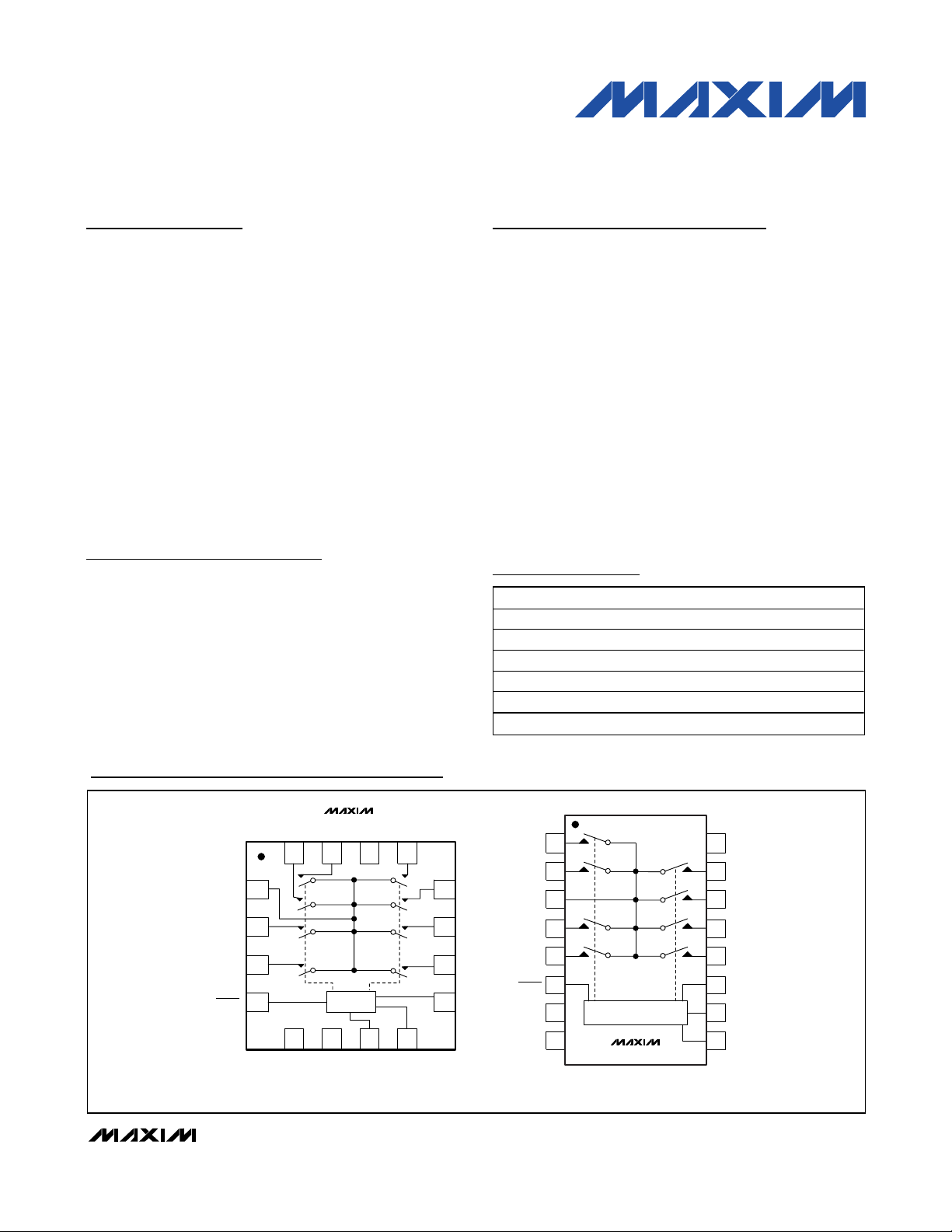
Pin Configurations/Functional Diagrams
PART TEMP RANGE PIN-PACKAGE
MAX4781EUE -40°C to +85°C 16 TSSOP
MAX4781ETE -40°C to +85°C 16 Thi n QFN ( 3m m x 3m m )
MAX4782EUE -40°C to +85°C 16 TSSOP
MAX4782ETE -40°C to +85°C 16 Thi n QFN ( 3m m x 3m m )
MAX4783EUE -40°C to +85°C 16 TSSOP
MAX4783ETE -40°C to +85°C
16 Thi n QFN ( 3m m x 3m m )
TOP VIEW
X
1
X7
2
X5
3
4
ENABLE
MAX4781
V
X4X6
CC
16 15 14 13
LOGIC
N.C.
3mm x 3mm THIN QFN
GND
CB
X2
X1
12
X0
11
X3
10
A
9
8765
ENABLE
N.C.
GND
1
X4
2
X6
3
X
X7
4
5
X5
6
7
8
LOGIC
MAX4781
TSSOP
16
V
CC
15
X2
14
X1
X0
13
12
X3
11
A
B
10
9
C
Page 2
MAX4781/MAX4782/MAX4783
High-Speed, Low-Voltage, 0.7Ω CMOS Analog
Switches/Multiplexers
2 _______________________________________________________________________________________
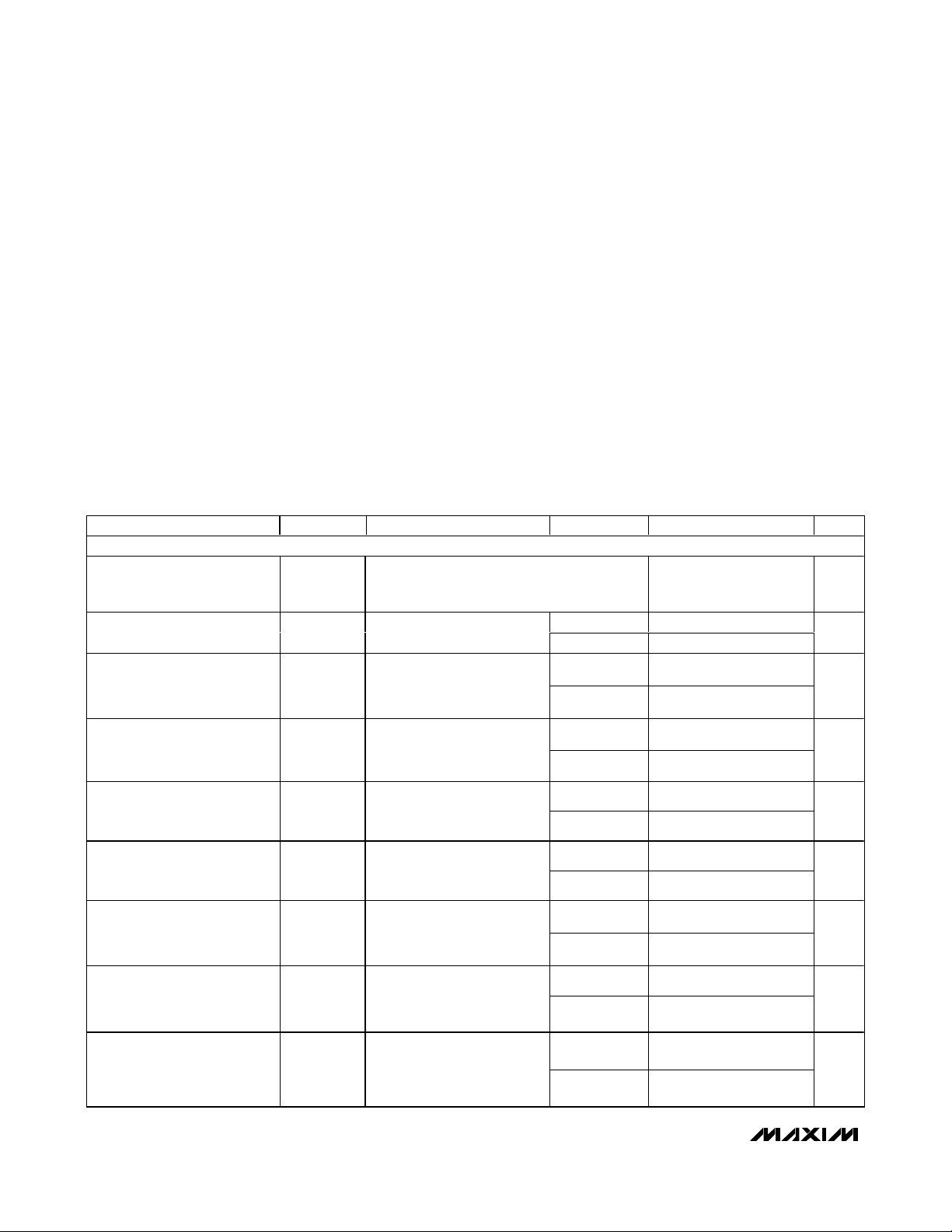
ABSOLUTE MAXIMUM RATINGS
ELECTRICAL CHARACTERISTICS—Single +3V Supply
(VCC= +2.7V to +3.6V, GND = 0, VIH= 1.4V, VIL= 0.5V, TA= T
MIN
to T
MAX
, unless otherwise noted. Typical values are at
T
A
= +25°C.) (Notes 2, 3)
Stresses beyond those listed under “Absolute Maximum Ratings” may cause permanent damage to the device. These are stress ratings only, and functional
operation of the device at these or any other conditions beyond those indicated in the operational sections of the specifications is not implied. Exposure to
absolute maximum rating conditions for extended periods may affect device reliability.
Voltages Referenced to GND
V
CC
, A, B, C, and ENABLE ...............................-0.3V to +4.6V
Voltage at Any Other Terminal
(Note 1)...................................................-0.3V to (V
CC
+ 0.3V)
Continuous Current into A, B, C, ENABLE........................±10mA
Continuous Current into X, Y, Z, X_, Y_, Z_ ....................±150mA
Peak Current into X, Y, Z, X_, Y_, Z_
(pulsed at 1ms, 10% duty cycle)................................±300mA
Continuous Power Dissipation
16-Pin Thin QFN (derate 16.9mW/°C above +70°C) ...1349mW
16-Pin TSSOP (derate 5.7mW/°C above +70°C) ........ 457mW
Operating Temperature Range ..........................-40°C to +85°C
Junction Temperature......................................................+150°C
Storage Temperature Range .............................-65°C to +150°C
Lead Temperature (soldering, 10s) .................................+300°C
Note 1: Signals on X, Y, Z, X_, Y_, and Z_ exceeding V
CC
or GND are clamped by internal diodes. Limit forward-diode current to
maximum current rating.
)
PARAMETER SYMBOL CONDITIONS T
ANALOG SWITCH
V
, VY, VZ,
Analog Signal Range
X
_, V Y_, VZ_
V
X
A
MIN TYP MAX UNITS
0V
CC
V
V
= + 2.7V ; I
On-Resistance (Note 4) R
ON
On-Resistance Match
Between Channels
(Notes 4, 5)
On-Resistance Flatness
(Note 6)
X_, Y_, Z_
Off-Leakage Current
X Off-Leakage Current
(MAX4781 Only)
X On-Leakage Current
(MAX4781 Only)
X, Y, Z Off-Leakage Current
(MAX4782/MAX4783 Only)
X, Y, Z On-Leakage Current
(MAX4782/MAX4783 Only)
∆R
R
FLAT(ON
I
X_(OFF)
I
Y_(OFF)
I
Z_(OFF)
I
X(OFF)
I
X(ON)
I
X(OFF)
I
Y(OFF)
I
Z(OFF)
I
X(ON)
I
Y(ON)
I
Z(ON)
ON
C C
100m A; V
V
= + 2.7V ; I
C C
100m A; V
V
= + 2.7V ; I
C C
100m A; V
1.7V
V
= + 3.6V ;
C C
V
, V Y_, V Z_ = 3.3V , 0.3V ; V X,
X _
, VZ = 0.3V, 3.3V
V
Y
V
= + 3.6V ;
C C
V
= 3.3V , 0.3V ;
X_
= 0.3V, 3.3V
V
X_
V
= +3.6V
C C
= 0.3V , 3.3V ;
V
X_
V
= 0.3V , 3.3V or fl oati ng
X_
V
= + 3.6V ;
C C
, V Y_, V Z_ = 3.3V , 0.3V ; V X,
V
X _
V
, VZ = 0.3V, 3.3V
Y
V
= + 3.6V ;
C C
V
, V Y, V Z = 0.3V , 3.3V ; VX, VY,
X
= 0.3V, 3.3V or floating
V
Z
, I
, I
X _
, VY, VZ = 1.7V
X
X _
, VY, VZ = 1.7V
X
X _
, VY, VZ = 0, 0.7V,
X
=
Y _
Z _
, I
, I
=
Y _
Z _
, I
, I
=
Y _
Z _
+25°C 0.7 1
T
MIN
to T
MAX
1.2
+25°C 0.3 0.4
T
MIN
to T
MAX
0.6
+25°C 0.1 0.2
T
MIN
to T
MAX
0.2
+25°C -2 0.002 +2
T
MIN
to T
MAX
-7 +7
+25°C -2 0.002 +2
T
MIN
to T
MAX
-50 +50
+25°C -2 0.002 +2
T
MIN
to T
MAX
-50 +50
+25°C -2 0.002 +2
T
MIN
to T
MAX
-25 +25
+25°C -2 0.002 +2
T
MIN
to T
MAX
-25 +25
Ω
Ω
Ω
nA
nA
nA
nA
nA
Page 3
MAX4781/MAX4782/MAX4783
High-Speed, Low-Voltage, 0.7Ω CMOS Analog
Switches/Multiplexers
_______________________________________________________________________________________ 3
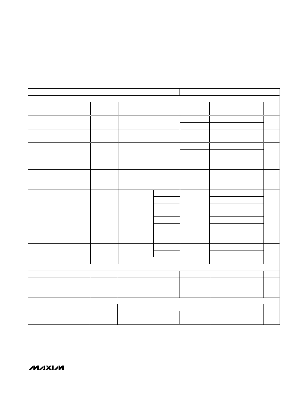
ELECTRICAL CHARACTERISTICS—Single +3V Supply (continued)
(VCC= +2.7V to +3.6V, GND = 0, VIH= 1.4V, VIL= 0.5V, TA= T
MIN
to T
MAX
, unless otherwise noted. Typical values are at TA=
+25°C.) (Notes 2, 3)
),
),
PARAMETER
SYMBOL
CONDITIONS T
SWITCH DYNAMIC CHARACTERISTICS
V
, V
, V
Turn-On Time t
Turn-Off Time t
Address Transition Time t
Break-Before-Make Time
(Note 7)
OFF
TRANS
t
BBM
Charge Injection Q
X_(OFF
Input Off-Capacitance
Output On-Capacitance
C
C
Y_(OFF
C
Z_(OFF)
C
X(OFF),
C
Y(OFF),
C
Z(OFF)
C
X(ON)
C
Y(ON)
C
Z(ON)
Off-Isolation (Note 8) V
Channel-to-Channel Crosstalk
(Note 9)
V
ON
ISO
CT
X _
= 35pF; Figure 1
C
L
V
, V
X _
C
= 35pF; Figure 1
L
V
, V
X _
C
= 35pF; Figure 2
L
V
, V
X _
C
= 35pF; Figure 3
L
V
GE N
Figure 4
f = 1MHz,
Figure 6
f = 1MHz,
Figure 6
f = 1MHz,
Figure 6
RL = 50Ω, CL =
35pF, Figure 5
RL = 50Ω, CL =
35pF, Figure 5
= 1.5V ; RL = 50Ω ;
Y _
Z _
, V
= 1.5V ; RL = 50Ω ;
Y _
Z _
, V
= 1.5V ; RL = 50Ω ;
Y _
Z _
, V
= 1.5V ; RL = 50Ω ;
Y _
Z _
= 0, R
GE N
Total Harmonic Distortion THD f = 20Hz to 20kHz, 0.5V
DIGITAL I/O
Input Logic High V
Input Logic Low V
Input Leakage Current IIN_
IH
IL
V
, VB, VC = V
A
3.6V
POWER SUPPLY
Power-Supply Range V
Positive Supply Current I
CC
CC
VCC = 3.6V; VA, VB, VC;
E N A B L E
= 3.6V or 0
V
A
+25°C 11 25
T
to T
MIN
MAX
+25°C 4 15
T
to T
MIN
MAX
+25°C 11 25
T
to T
MIN
MAX
+25°C 18
T
to T
MIN
MAX
= 0, C L = 1nF,
+25°C -110 pC
+25°C 38 pF
MAX4781 310
MAX4782 158Output Off-Capacitance
+25°C
MAX4783
MAX4781 380
MAX4782 224
+25°C
MAX4783
f = 10MHz -75
f = 1MHz -90
f = 10MHz -65
f = 1MHz -80
, RL = 32Ω 0.045 %
P-P
T
to T
E N A B L E
= 0 or
T
T
MIN
MIN
MIN
to T
to T
MAX
MAX
MAX
MIN TYP MAX UNITS
27
20
27
2
ns
ns
ns
ns
pF
75
pF
140
dB
dB
1.4 V
0.5 V
-1 0.0005 +1 µA
+1.6 +3.6 V
1µA
Page 4
MAX4781/MAX4782/MAX4783
High-Speed, Low-Voltage, 0.7Ω CMOS Analog
Switches/Multiplexers
4 _______________________________________________________________________________________
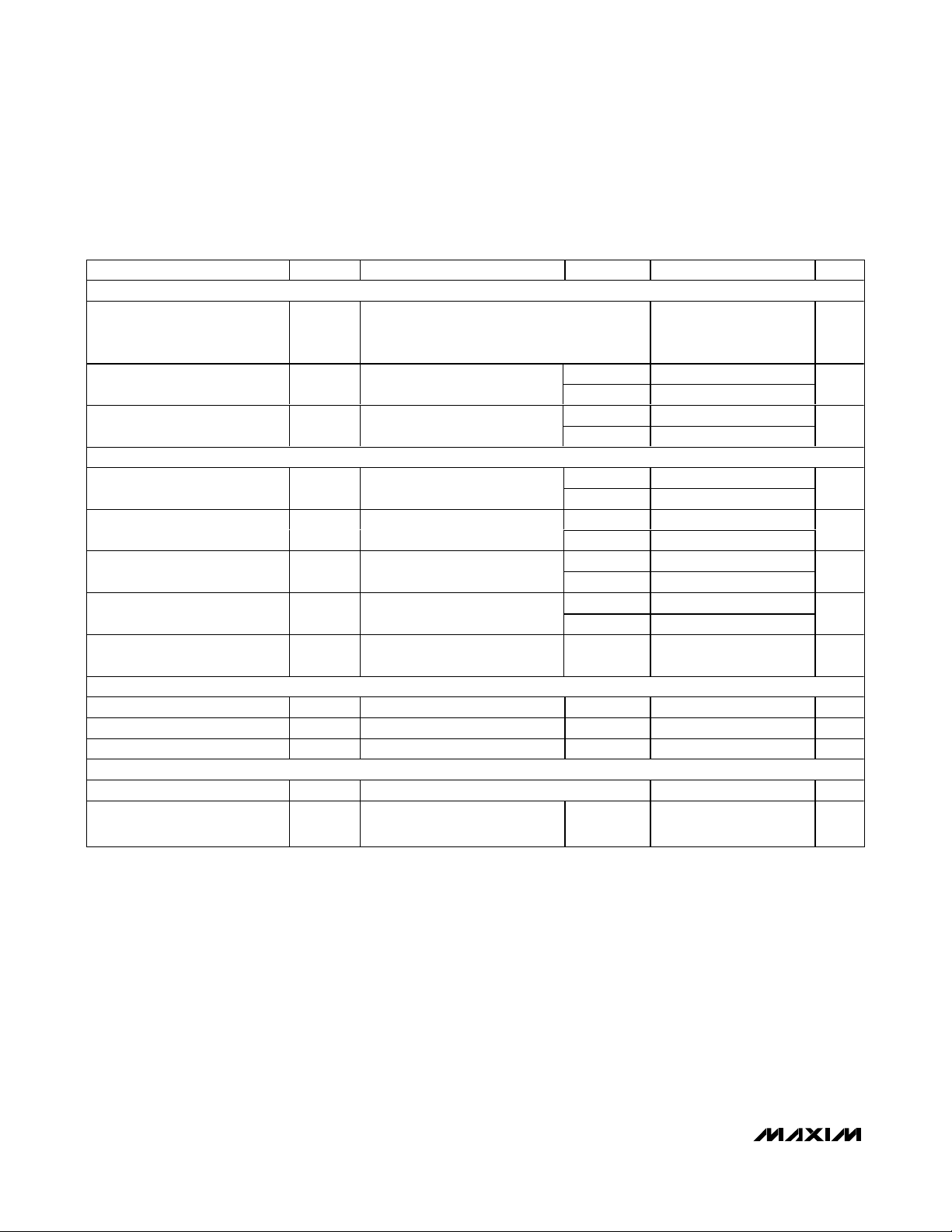
ELECTRICAL CHARACTERISTICS—Single +1.8V Supply
(VCC= +1.8V, GND = 0, VIH= 1V, VIL= 0.4V, TA= T
MIN
to T
MAX
, unless otherwise noted. Typical values are at TA= +25°C.) (Notes 2, 3)
Note 2: The algebraic convention is used in this data sheet; the most negative value is shown in the minimum column.
Note 3: Devices are tested at maximum hot temperature and are guaranteed by design and correlation at T
A
= +25°C and -40°C
specifications.
Note 4: R
ON
and ∆RONmatching specifications for thin QFN-packaged parts are guaranteed by design.
Note 5: ∆R
ON
= R
ON(MAX)
- R
ON(MIN).
Note 6: Flatness is defined as the difference between the maximum and minimum value of on-resistance as measured over the
specified analog signal ranges.
Note 7: Guaranteed by design; not production tested.
Note 8: Off-isolation = 20log10(V
COM_
/ VNO), V
COM_
= output, VNO= input to off switch.
Note 9: Between any two channels.
PARAMETER SYMBOL CONDITIONS T
ANALOG SWITCH
_, V Y _ ,
V
X
_, V X ,
Analog Signal Range
On-Resistance (Note 4) R
On-Resistance Match Between
Channels (Notes 4, 5)
V
Z
V
, V
Y
Z
ON
∆R
ON
SWITCH DYNAMIC CHARACTERISTICS
Turn-On Time t
Turn-Off Time t
Address Transition Time t
Break-Before-Make Time
(Note 7)
ON
OFF
TRANS
t
BBM
Charge Injection Q
DIGITAL I/O
Input Logic High V
Input Logic Low V
IH
IL
Input Leakage Current IIN_V A, VB, VC = V
POWER SUPPLY
Power-Supply Range V
Positive Supply Current I
CC
CC
VCC = 1.8V; IX_, IY_, IZ_ = 10mA;
V
, VY, VZ = 1.0V
X
VCC = 1.8V; IX_, IY_, IZ_ = 10mA;
V
, VY, VZ = 1.0V
X
VX_, VY_, VZ_ = 1.0V; RL = 50Ω;
= 35pF; Figure 1
C
L
VX_, VY_, VZ_ = 1.0V; RL = 50Ω;
= 35pF; Figure 1
C
L
VX_, VY_, VZ_ = 1.0V; RL = 50Ω;
= 35pF; Figure 2
C
L
VX_, VY_, VZ_ = 1V; RL = 50Ω;
C
= 35pF; Figure 3
L
V
GEN
= 0, R
= 0, CL = 1nF,
GEN
Figure 4
E N A B L E
= 0 or 3.6V T
VCC = 3.6V; VA, VB, VC,
V
E N A B L E
= 0 or 3.6V
A
MIN TYP MAX UNITS
0V
+25°C 1.6 2.5
T
to T
M IN
M AX
+25°C 0.3 0.4
T
to T
M IN
M AX
+25°C 17 30
T
to T
M IN
M AX
+25°C 8 20
T
to T
M IN
M AX
+25°C 17 30
T
to T
M IN
M AX
+25°C 26
T
M IN
to T
M AX
1
+25°C -40 pC
T
T
M IN
M IN
M IN
to T
to T
to T
M AX
M AX
M AX
1V
0.000
-1
1.6 3.6 V
CC
3.5
0.6
32
22
32
V
Ω
Ω
ns
ns
ns
ns
0.4 V
+1 µA
1µA
Page 5
MAX4781/MAX4782/MAX4783
High-Speed, Low-Voltage, 0.7Ω CMOS Analog
Switches/Multiplexers
_______________________________________________________________________________________ 5
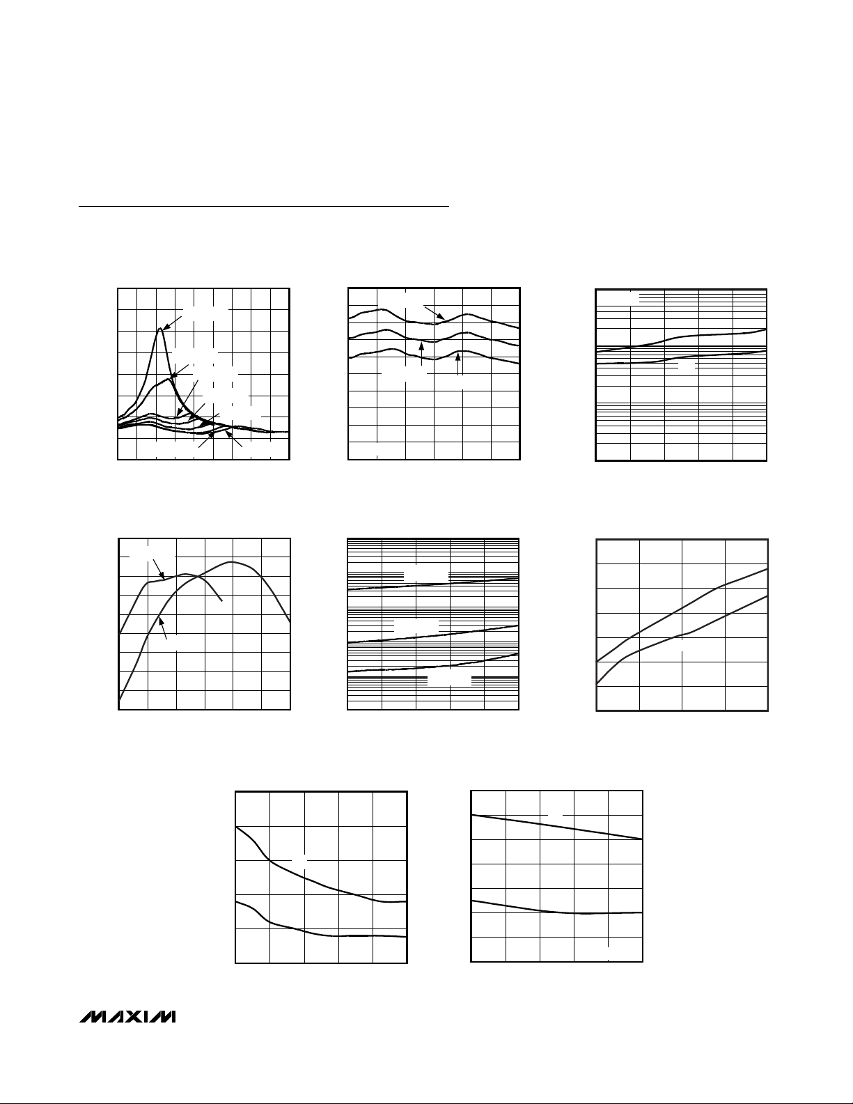
Typical Operating Characteristics
(GND = 0, TA = +25°C, unless otherwise noted.)
ON-RESISTANCE vs. VX, VY, V
2.0
1.8
1.6
1.4
(Ω)
1.2
ON
R
1.0
0.8
0.6
0.4
0 3.6
VCC = 1.8V
VCC = 2.0V
VCC = 2.5V
VCC = 2.7V
VCC = 3.0V
VCC = 3.3V
VX, VY, VZ (V)
CHARGE INJECTION vs. VX, VY, V
60
VCC = 1.8V
40
20
0
-20
-40
-60
CHARGE INJECTION (pC)
-80
-100
-120
VCC = 3.0V
0 3.0
VX, VY, VZ (V)
Z
MAX4781 toc01
VCC = 3.6V
3.22.80.4 0.8 1.2 2.01.6 2.4
Z
MAX4781 toc04
2.50.5 1.0 1.5 2.0
ON-RESISTANCE vs. VX, VY, VZ,
1.0
0.9
0.8
0.7
0.6
(Ω)
0.5
ON
R
0.4
0.3
0.2
0.1
0
0 3.0
1000
100
10
(nA)
CC
I
1
0.1
0.01
1.6 2.0 2.4 2.8 3.2 3.6
AND TEMPERATURE
TA = +85°C
TA = +25°C
VCC = 3.0V
TA = -40°C
VX, VY, VZ (V)
SUPPLY CURRENT vs. TEMPERATURE
TA = +85°C
TA = +25°C
TA = -40°C
VCC (V)
LEAKAGE CURRENT vs. TEMPERATURE
1000
VCC = 3.6V
MAX4781 toc02
100
(pA)
Z
, I
Y
, I
X
I
10
2.50.5 1.0 1.5 2.0
1
-40 856010 35-15
ON
OFF
TEMPERATURE (°C)
LOGIC THRESHOLD
vs. SUPPLY VOLTAGE
1.2
MAX4781 toc05
1.1
1.0
0.9
0.8
LOGIC THRESHOLD (V)
0.7
0.6
0.5
1.6 3.6
RISING
FALLING
2.1 2.6 3.1
SUPPLY VOLTAGE (V)
MAX4781toc03
MAX4781 toc06
TURN-ON/TURN-OFF TIME
vs. SUPPLY VOLTAGE
25
20
15
TIME (ns)
10
5
0
1.6 3.6
t
ON
t
OFF
2.0 2.4 2.8 3.2
SUPPLY VOLTAGE (V)
MAX4781 toc07
14
12
10
8
TIME (ns)
6
4
2
0
TURN-ON/TURN-OFF TIME
vs. TEMPERATURE
t
ON
t
OFF
VCC = 3.0V
-40 85
-15 10 35 60
TEMPERATURE (°C)
MAX4781 toc08
Page 6
MAX4781/MAX4782/MAX4783
High-Speed, Low-Voltage, 0.7Ω CMOS Analog
Switches/Multiplexers
6 _______________________________________________________________________________________
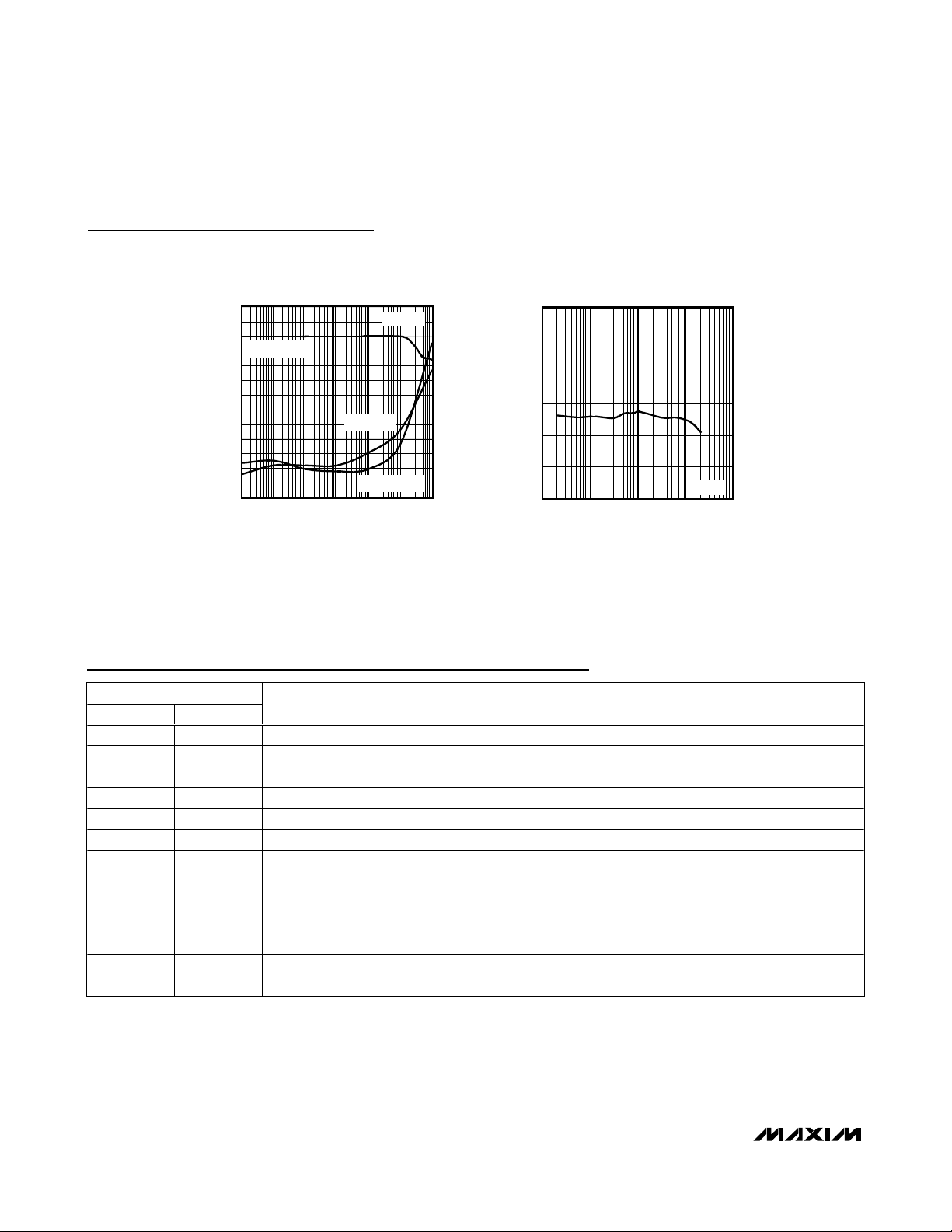
Typical Operating Characteristics (continued)
(GND = 0, TA = +25°C, unless otherwise noted.)
MAX4781 Pin Description
FREQUENCY RESPONSE
FREQUENCY (Hz)
100 100k 1M 10M1k 10k 100M
RESPONSE (dB)
-110
-90
-70
-50
-30
10
-10
VCC = 3V
ON-RESPONSE
CROSSTALK
OFF-ISOLATION
MAX4781 toc09
0.08
0.02
10 1k 10k100 100k
TOTAL HARMONIC DISTORTION
vs. FREQUENCY
MAX4781 toc10
FREQUENCY (Hz)
THD (%)
0.03
0.04
0.05
0.06
0.07
VCC = 3V
TSSOP THIN QFN
PIN
NAME FUNCTION
3 1 X Analog Switch Output
64ENABLE
Digital Enable Input. Normally connect to GND. Drive to logic high to set all switches
off.
7 5 N.C. No Connection. Not internally connected.
8 6 GND Ground
9 7 C Digital Address C Input
10 8 B Digital Address B Input
11 9 A Digital Address A Input
13, 14, 15,
12, 1, 5, 2,
4
16 14 V
— EP PAD Exposed Pad. Connect to GND.
11, 12, 13,
10, 15, 3,
16, 2
X0–X7 Analog Switch Inputs X0–X7
Positive Analog and Digital Supply Voltage Input
CC
Page 7
MAX4781/MAX4782/MAX4783
High-Speed, Low-Voltage, 0.7Ω CMOS Analog
Switches/Multiplexers
_______________________________________________________________________________________ 7
MAX4782 Pin Description
MAX4783 Pin Description
PIN
TSSOP THIN QFN
1, 5, 2, 4 15, 3, 16, 2 Y0–Y3 Analog Switch Y Inputs Y0–Y3
3 1 Y Analog Switch Y Output
64ENABLE
7 5 N.C. No Connection. Not internally connected.
8 6 GND Ground
9 7 B Digital Address B Input
10 8 A Digital Address A Input
12, 14, 15, 11 10, 12, 13, 9 X0–X3 Analog Switch X Inputs X0–X3
13 11 X Analog Switch X Output
16 14 V
PIN
TSSOP THIN QFN
1 15 Y1 Analog Switch Y Normally Open Input
2 16 Y0 Analog Switch Y Normally Closed Input
3 1 Z1 Analog Switch Z Normally Open Input
4 2 Z Analog Switch Z Output
5 3 Z0 Analog Switch Z Normally Closed Input
64ENABLE
7 5 N.C. No Connection. Not internally connected.
8 6 GND Ground
9 7 C Digital Address C Input
10 8 B Digital Address B Input
11 9 A Digital Address A Input
12 10 X0 Analog Switch X Normally Closed Input
13 11 X1 Analog Switch X Normally Open Input
14 12 X Analog Switch X Output
15 13 Y Analog Switch Y Output
16 14 V
NAME FUNCTION
Digital Enable Input. Normally connect to GND. Drive to logic high to set all
switches off.
CC
NAME FUNCTION
CC
Positive Analog and Digital Supply Voltage Input
Digital Enable Input. Normally connect to GND. Drive to logic high to set all
switches off.
Positive Analog and Digital Supply Voltage Input
Page 8

MAX4781/MAX4782/MAX4783
High-Speed, Low-Voltage, 0.7Ω CMOS Analog
Switches/Multiplexers
8 _______________________________________________________________________________________
Applications Information
Power-Supply Considerations
Overview
The MAX4781/MAX4782/MAX4783 construction is typical
of most CMOS analog switches. There are two supply
inputs: V
CC
and GND. VCCand GND drive the internal
CMOS switches and set the limits of the analog voltage
on any switch. Internal reverse ESD-protection diodes are
connected between each analog signal input and both
V
CC
and GND. If any analog signal exceeds VCCor
GND, one of these diodes conducts. During normal operation, these and other reverse-biased ESD diodes leak,
forming the only current drawn from VCCor GND.
Virtually all the analog leakage current comes from the
ESD diodes. Although the ESD diodes on a given signal input are identical and therefore fairly well balanced, they are reverse-biased differently. Each diode
is biased by either VCCor GND and the analog signal.
Their leakages vary as the signal varies. The difference
in the two diodes’ leakages to VCCand GND constitutes the analog-signal-path leakage current. All analog
leakage current flows between each input and one of
the supply terminals, not to the other switch terminal.
Both sides of a given switch can show leakage currents
of either the same or opposite polarity.
VCCand GND power the internal logic and set the input
logic limits. Logic inputs have ESD-protection diodes
to ground.
Power Supply
The MAX4781/MAX4782/MAX4783 operate from a single supply between +1.6V and +3.6V. Switch on-resistance increases as the supply voltage is lowered.
High-Frequency Performance
In 50Ω systems, signal response is reasonably flat up
to 50MHz (see the Typical Operating Characteristics).
Above 20MHz, the on-response has several minor
peaks that are highly layout dependent. In the off state,
the switch acts like a capacitor and passes higher frequencies with less attenuation. At 10MHz, off-isolation
is approximately -50dB in 50Ω systems, becoming
worse (approximately 20dB per decade) as frequency
increases. Higher circuit impedance also degrades offisolation. Adjacent channel attenuation is approximately 3dB above that of a bare IC socket and is entirely
because of capacitive coupling.
Pin Nomenclature
The MAX4781/MAX4782/MAX4783 are pin compatible
with the industry-standard 74HC4051/74HC4052/
74HC4053 and the MAX4617/MAX4618/MAX4619. In
single-supply applications, they function identically and
have identical logic diagrams, although these parts differ electrically. The pin designations and logic diagrams in this data sheet conform to the original 1972
specifications published by RCA for the CD4051/
CD4052/CD4053. These designations differ from the
standard Maxim switch and mux designations found on
other Maxim data sheets such as the MAX4051/
MAX4052/MAX4053. Designers who are more comfortable with Maxim’s standard designations are advised
that the pin designations and logic diagrams on the
MAX4051/MAX4052/MAX4053 data sheet can be
applied to the MAX4781/MAX4782/MAX4783.
Page 9

✓ = Don’t care.
*Not present on MAX4782.
Note: Input and output pins are identical and interchangeable. Either can be considered an input or output. Signals pass equally
well in either direction.
Table 1. Truth Table/Switch Programming
MAX4781/MAX4782/MAX4783
High-Speed, Low-Voltage, 0.7Ω CMOS Analog
Switches/Multiplexers
_______________________________________________________________________________________ 9
ENABLE
INPUT
H
LLLL X-X0
L L L H X-X1
L L H L X-X2
L L H H X-X3
L H L L X-X4
L H L H X-X5
C* B A MAX4781 MAX4782 MAX4783
✓✓✓All switches open All switches open All switches open
SELECT INPUT ON SWITCHES
X-X0
Y-Y0
X-X1
Y-Y1
X-X2
Y-Y2
X-X3
Y-Y3
X-X0
Y-Y0
X-X1
Y-Y1
X-X0
Y-Y0
Z-Z0
X-X1
Y-Y0
Z-Z0
X-X0
Y-Y1
Z-Z0
X-X1
Y-Y1
Z-Z0
X-X0
Y-Y0
Z-Z1
X-X1
Y-Y0
Z-Z1
L H H L X-X6
L H H H X-X7
X-X2
Y-Y2
X-X3
Y-Y3
X-X0
Y-Y1
Z-Z1
X-X1
Y-Y1
Z-Z1
Page 10
MAX4781/MAX4782/MAX4783
High-Speed, Low-Voltage, 0.7Ω CMOS Analog
Switches/Multiplexers
10 ______________________________________________________________________________________
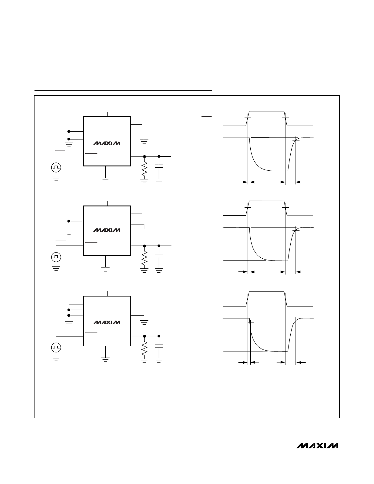
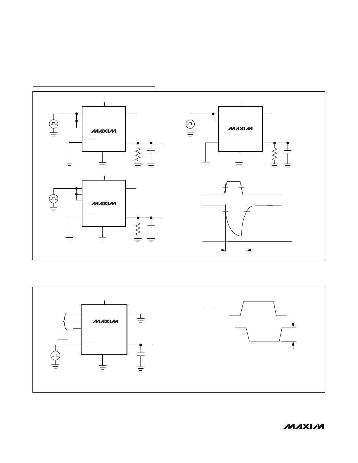
Test Circuits/Timing Diagrams
Figure 1. Enable Switching Times
V
V
ENABLE
V
ENABLE
A
B
C
MAX4781
ENABLE
GND
A
B
X1, X2, X3, Y1, Y2, Y3
MAX4782
ENABLE
GND
CC
V
CC
X0
X1–X7
X
V
CC
V
CC
X0, Y0
X, Y
50Ω
50Ω
V
CC
V
OUT
35pF
V
CC
V
OUT
35pF
V
ENABLE
V
ENABLE
V
CC
0
V
X0
V
OUT
0
t
OFF
V
CC
0
,
V
X0
V
Y0
V
OUT
0
50%
90%
50%
90%
90%
90%
t
ON
V
CC
V
A
B
C
V
ENABLE
TEST EACH SECTION INDIVIDUALLY.
ENABLE
V
MAX4783
GND
CC
X1, Y1, Z1
X0, Y0, Z0
X, Y, Z
50Ω
V
CC
V
OUT
35pF
ENABLE
V
OUT
V
VX0,
V
V
VX1,
V
V
t
OFF
CC
0
,
Y0
Z0
,
Y1
Z1
t
OFF
50%
90%
90%
t
ON
t
ON
Page 11

MAX4781/MAX4782/MAX4783
High-Speed, Low-Voltage, 0.7Ω CMOS Analog
Switches/Multiplexers
______________________________________________________________________________________ 11
Test Circuits/Timing Diagrams (continued)
Figure 2. Address Transition Times
VA, VB, VC
V
, V
A
B
A
B
C
ENABLE
A
B
ENABLE
V
CC
V
CC
MAX4781
GND
V
CC
V
CC
MAX4782
GND
X1–X7
X0, Y0
X1, X2, Y1,
Y2, X3, Y3
X, Y
tR < 5ns
< 5ns
t
V
OUT
OUT
CC
C
0
V
X0
V
X7
t
TRANS
V
CC
B
0
V
,
X0
V
Y0
VX3,
V
Y3
t
TRANS
VA, VB, V
X0
X
V
CC
V
OUT
35pF
V
50Ω
VA, V
V
CC
V
50Ω
OUT
35pF
V
50%
10%
50%
10%
F
90%
90%
t
TRANS
t
TRANS
V
V
, VB, V
A
C
A
V
B
C
MAX4783
ENABLE
GND
TEST EACH SECTION INDIVIDUALLY.
CC
CC
X1, Y1, Z1
X0, Y0, Z0
X, Y, Z
50Ω
VA, VB, V
CC
C
50%
V
0
V
,
X0
,
V
Y0
V
OUT
VX1,
V
V
Z0
,
Y1
Z1
t
TRANS
10%
V
CC
V
OUT
35pF
V
90%
t
TRANS
Page 12
MAX4781/MAX4782/MAX4783
High-Speed, Low-Voltage, 0.7Ω CMOS Analog
Switches/Multiplexers
12 ______________________________________________________________________________________
Test Circuits/Timing Diagrams (continued)
Figure 3. Break-Before-Make Interval
Figure 4. Charge Injection
V
CC
VA, VB, V
C
A
B
C
V
CC
X0–X7
V
CC
VA, V
MAX4781
V
35pF
35pF
OUT
VA, VB, V
V
OUT
V+
C
, VY, V
V
X
V
OUT
ENABLE
GND
V
VA, VB, V
C
A
B
C
V
MAX4783
ENABLE
GND
TEST EACH SECTION INDIVIDUALLY.
CC
CC
X0, X1, Y0,
Y1, Z0, Z1
X, Y, Z
X
50Ω
V
CC
50Ω
V
CC
B
A
B
V
CC
X0–X3,
Y0–Y3
V
CC
MAX4782
ENABLE
GND
50%
0
Z
0
t
BBM
t
R
t
F
X, Y
< 5ns
< 5ns
90%
50Ω
35pF
V
OUT
V
CHANNEL
SELECT
B
C
A
V
ENABLE
ENABLE
TEST EACH SECTION INDIVIDUALLY.
CC
V
CC
X_, Y_, Z_
MAX4781
MAX4782
MAX4783
GND
X, Y, Z
C
L
1000pF
V
ENABLE
V
OUT
V
CC
0
V
OUT
∆V
IS THE MEASURED VOLTAGE DUE TO CHARGE-
OUT
TRANSFER ERROR Q WHEN THE CHANNEL TURNS OFF.
Q = ∆V
✕ C
OUT
L
∆V
OUT
Page 13
MAX4781/MAX4782/MAX4783
High-Speed, Low-Voltage, 0.7Ω CMOS Analog
Switches/Multiplexers
______________________________________________________________________________________ 13
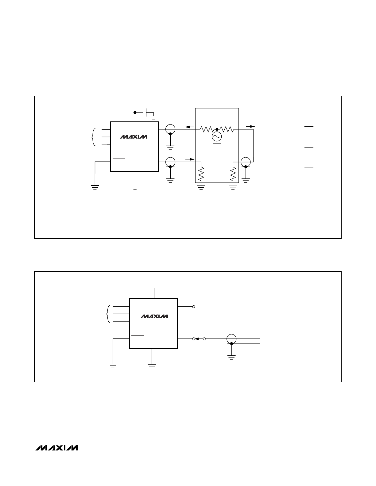
Test Circuits/Timing Diagrams (continued)
Figure 5. Off-Isolation, On-Loss, and Crosstalk
Figure 6. Capacitance
Chip Information
TRANSISTOR COUNT: 659
PROCESS: CMOS
V
CC
V
CC
MAX4781
MAX4782
CHANNEL
SELECT
A
B
C
MAX4783
ENABLE
GND
NOTES: MEASUREMENTS ARE STANDARDIZED AGAINST SHORT AT SOCKET TERMINALS.
OFF-ISOLATION IS MEASURED BETWEEN COM AND "OFF" NO TERMINAL ON EACH SWITCH.
ON-LOSS IS MEASURED BETWEEN COM AND "ON" NO TERMINAL ON EACH SWITCH.
CROSSTALK IS MEASURED BETWEEN ADJACENT CHANNELS WITH ONE CHANNEL ON AND THE OTHER OFF.
SIGNAL DIRECTION THROUGH SWITCH IS REVERSED; WORST VALUES ARE RECORDED.
10nF
X_, Y_, Z_
X, Y, Z
NETWORK
V
IN
V
OUT
50Ω
MEAS.
50Ω 50Ω
ANALYZER
50Ω
REF.
OFF-ISOLATION = 20log
ON-LOSS = 20log
CROSSTALK = 20log
V
OUT
V
IN
V
OUT
V
IN
V
OUT
V
IN
V
CC
V
CC
CHANNEL
SELECT
A
B
C
X_, Y_, Z_
MAX4781
MAX4782
ENABLE
MAX4783
GND
X, Y, Z
1MHz
CAPACITANCE
ANALYZER
Page 14

MAX4781/MAX4782/MAX4783
High-Speed, Low-Voltage, 0.7Ω CMOS Analog
Switches/Multiplexers
14 ______________________________________________________________________________________
Pin Configurations/Functional Diagrams (continued)
TOP VIEW
Y
Y3
Y1
ENABLE
16 15 14 13
1
2
3
4
N.C.
MAX4782
Y0Y2
LOGIC
GND
V
CC
X2
8765
BA
X1
12
X
11
X0
10
X3
9
3mm x 3mm THIN QFN
MAX4783
Y1Y0
16 15 14 13
Z1
1
V
cc
Y
12
X
ENABLE
N.C.
GND
1
Y0
2
Y2
3
Y
Y3
4
5
Y1
6
7
8
LOGIC
16
V
CC
15
X2
14
X1
13
X
12
X0
11
X3
10
A
9
B
MAX4782
TSSOP
1
Y1
2
Y0
3
Z1
MAX4783
16
V
CC
15
Y
14
X
2
Z
Z0
ENABLE
3
4
8765
N.C.
GND
CB
3mm X 3mm THIN QFN
11
X1
10
X0
9
A
ENABLE
N.C.
GND
Z
4
5
Z0
6
7
8
TSSOP
X1
13
12
X0
11
A
10
B
9
C
Page 15

MAX4781/MAX4782/MAX4783
High-Speed, Low-Voltage, 0.7Ω CMOS Analog
Switches/Multiplexers
______________________________________________________________________________________ 15
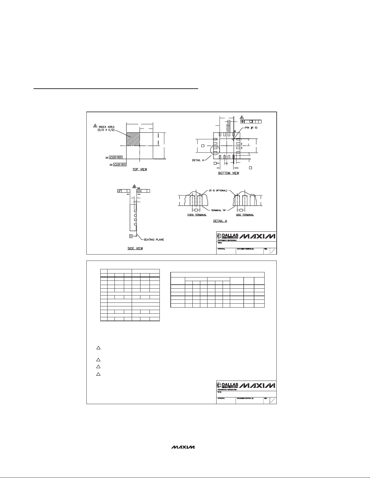
Package Information
(The package drawing(s) in this data sheet may not reflect the most current specifications. For the latest package outline information,
go to www.maxim-ic.com/packages.)
TSSOP4.40mm.EPS
Page 16
MAX4781/MAX4782/MAX4783
High-Speed, Low-Voltage, 0.7Ω CMOS Analog
Switches/Multiplexers
Maxim cannot assume responsibility for use of any circuitry other than circuitry entirely embodied in a Maxim product. No circuit patent licenses are
implied. Maxim reserves the right to change the circuitry and specifications without notice at any time.
16 ____________________Maxim Integrated Products, 120 San Gabriel Drive, Sunnyvale, CA 94086 408-737-7600
© 2005 Maxim Integrated Products Printed USA is a registered trademark of Maxim Integrated Products, Inc.
Package Information (continued)
(The package drawing(s) in this data sheet may not reflect the most current specifications. For the latest package outline information,
go to www.maxim-ic.com/packages.)
D2
b
0.10 M
D
D/2
D2/2
C A B
E/2
C
L
C
L
0.10 C 0.08 C
PKG
REF. MIN.
A
b
D
E
e
L
N
ND
NE
A1
A2
k
0.70
0.20
2.90
2.90
0.45
0
0.25
12L 3x3
NOM. MAX. NOM.
0.75
0.25
3.00
3.00
0.50 BSC.
0.55
12
3
0.0230.05
0.20 REF
-
MIN. MAX.
0.80
0.70
0.30
0.20
3.10
2.90
2.90
3.10
0.30
0.65
-
0.25
A
A2
A1
16L 3x3
0.75
0.25
3.00
3.00
0.50 BSC.
0.40
16
4
4
0.02
0
0.20 REF
-
E
0.80
0.30
3.10
3.10
0.50
0.05
-
PKG.
CODES
T1233-1
T1233-3
T1633-1 0.95
T1633-2
T1633F-3 0.65
T1633-4
(NE - 1) X e
C
L
L
e
EXPOSED PAD VARIATIONS
D2
MIN.
NOM.
1.10
0.95
1.10
0.95
1.10
0.95
1.10
0.80
0.95
1.10
MAX.
1.25
1.25
1.25
1.25
0.95
1.25
e
MIN.
0.95
0.95 1.10
0.95
0.95
0.65
0.95
NOM.
1.10
1.10
1.10
0.80
1.10
E2
E2/2
L
k
(ND - 1) X e
C
L
e
PACKAGE OUTLINE
12, 16L, THIN QFN, 3x3x0.8mm
21-0136
PIN ID
MAX.
1.25
1.25
1.25
0.95
1.25
JEDEC
0.35 x 45∞
WEED-1
0.35 x 45∞1.25 WEED-1
0.35 x 45∞ WEED-2
0.35 x 45∞
WEED-2
0.225 x 45∞
WEED-2
0.35 x 45∞
WEED-2
E2
DOWN
BONDS
ALLOWED
NO
YES
NO
YES
N/A
NO
12x16L QFN THIN.EPS
L
1
E
2
NOTES:
1. DIMENSIONING & TOLERANCING CONFORM TO ASME Y14.5M-1994.
2. ALL DIMENSIONS ARE IN MILLIMETERS. ANGLES ARE IN DEGREES.
3. N IS THE TOTAL NUMBER OF TERMINALS.
4. THE TERMINAL #1 IDENTIFIER AND TERMINAL NUMBERING CONVENTION SHALL CONFORM TO
JESD 95-1 SPP-012. DETAILS OF TERMINAL #1 IDENTIFIER ARE OPTIONAL, BUT MUST BE LOCATED
WITHIN THE ZONE INDICATED. THE TERMINAL #1 IDENTIFIER MAY BE EITHER A MOLD OR
MARKED FEATURE.
5. DIMENSION b APPLIES TO METALLIZED TERMINAL AND IS MEASURED BETWEEN 0.20 mm AND 0.25 mm
FROM TERMINAL TIP.
6. ND AND NE REFER TO THE NUMBER OF TERMINALS ON EACH D AND E SIDE RESPECTIVELY.
7. DEPOPULATION IS POSSIBLE IN A SYMMETRICAL FASHION.
8. COPLANARITY APPLIES TO THE EXPOSED HEAT SINK SLUG AS WELL AS THE TERMINALS.
9. DRAWING CONFORMS TO JEDEC MO220 REVISION C.
PACKAGE OUTLINE
12, 16L, THIN QFN, 3x3x0.8mm
21-0136
2
E
2
 Loading...