

_______________General Description
The MAX477 is a ±5V wide-bandwidth, fast-settling,
unity-gain-stable op amp featuring low noise, low differential gain and phase errors, high slew rate, high precision, and high output current. The MAX477’s architecture uses a standard voltage-feedback topology that
can be configured into any desired gain setting, as with
other general-purpose op amps.
Unlike high-speed amplifiers using current-mode feedback architectures, the MAX477 has a unique input
stage that combines the benefits of the voltage-feedback design (flexibility in choice of feedback resistor,
two high-impedance inputs) with those of the currentfeedback design (high slew rate and full-power bandwidth). It also has the precision of voltage-feedback
amplifiers, characterized by low input-offset voltage
and bias current, low noise, and high common-mode
and power-supply rejection.
The MAX477 is ideally suited for driving 50Ω or 75Ω
loads. Available in DIP, SO, space-saving µMAX, and
SOT23 packages.
________________________Applications
Broadcast and High-Definition TV Systems
Video Switching and Routing
Communications
Medical Imaging
Precision DAC/ADC Buffer
____________________________Features
♦ High Speed:
300MHz -3dB Bandwidth (A
V
= +1)
200MHz Full-Power Bandwidth (A
V
= +1, Vo = 2Vp-p)
1100V/µs Slew Rate
130MHz 0.1dB Gain Flatness
♦ Drives 100pF Capacitive Loads Without Oscillation
♦ Low Differential Phase/Gain Error: 0.01°/0.01%
♦ 8mA Quiescent Current
♦ Low Input-Referred Voltage Noise: 5nV/
√
HHzz
♦ Low Input-Referred Current Noise: 2pA/
√
HHzz
♦ Low Input Offset Voltage: 0.5mV
♦ 8000V ESD Protection
♦ Voltage-Feedback Topology for Simple Design
Configurations
♦ Short-Circuit Protected
♦ Available in Space-Saving SOT23 Package
MAX477
300MHz High-Speed Op Amp
________________________________________________________________
Maxim Integrated Products
1
19-0467; Rev 2; 5/97
PART
MAX477EPA
MAX477ESA
MAX477EUA -40°C to +85°C
-40°C to +85°C
-40°C to +85°C
TEMP. RANGE
PIN-
PACKAGE
8 Plastic DIP
8 SO
8 µMAX
EVALUATION KIT MANUAL
AVAILABLE
______________Ordering Information
OUT
IN+
N.C.
V
EE
1
2
8
7
N.C.
V
CC
IN-
N.C.
DIP/SO/µMAX
TOP VIEW
3
4
6
5
V
EE
IN-IN+
15V
CC
OUT
MAX477
MAX477
SOT23-5
2
34
__________________Pin Configuration
V
IN
VIDEO/RF CABLE DRIVER
500Ω
500Ω
75Ω
75Ω
V
OUT
75Ω
MAX477
__________Typical Operating Circuit
MAX477MJA -55°C to +125°C 8 CERDIP
MAX477EUK-T -40°C to +85°C 5 SOT23
SOT
TOP
MARK
—
—
—
—
ABYW
For free samples & the latest literature: http://www.maxim-ic.com, or phone 1-800-998-8800.
For small orders, phone 408-737-7600 ext. 3468.
Open-Loop Voltage Gain
MAX477
300MHz High-Speed Op Amp
2 _______________________________________________________________________________________
ABSOLUTE MAXIMUM RATINGS
DC ELECTRICAL CHARACTERISTICS
(VCC= +5V, VEE= -5V, V
OUT
= 0V, RL= ∞, TA= T
MIN
to T
MAX,
unless otherwise noted. Typical values are at TA= +25°C.) (Note 1)
Stresses beyond those listed under “Absolute Maximum Ratings” may cause permanent damage to the device. These are stress ratings only, and functional
operation of the device at these or any other conditions beyond those indicated in the operational sections of the specifications is not implied. Exposure to
absolute maximum rating conditions for extended periods may affect device reliability.
Supply Voltage (VCCto VEE)..................................................12V
Differential Input Voltage..................(V
CC
+ 0.3V) to (VEE- 0.3V)
Common-Mode Input Voltage..........(V
CC
+ 0.3V) to (VEE- 0.3V)
Output Short-Circuit Duration to GND........................Continuous
Continuous Power Dissipation (T
A
= +70°C)
Plastic DIP (derate 9.09mW/°C above +70°C)..............727mW
SO (derate 5.88mW/°C above +70°C)..........................471mW
µMAX (derate 4.1mW/°C above +70°C) .......................330mW
CERDIP (derate 8.00mW/°C above +70°C)..................640mW
SOT23 (derate 7.1mW/°C above +70°C)......................571mW
Operating Temperature Ranges
MAX477E_A......................................................-40°C to +85°C
MAX477EUK.....................................................-40°C to +85°C
MAX477MJA...................................................-55°C to +125°C
Storage Temperature Range.............................-65°C to +160°C
Lead Temperature (soldering, 10sec).............................+300°C
MAX477ESA/EPA/EUA/MJA
MAX477MJA, TA= T
MIN
to T
MAX
MAX477E_ _, TA= T
MIN
to T
MAX
TA= +25°C
V
OUT
= 0, f = DC
TA= T
MIN
to T
MAX
TA= +25°C
Short to ground
Either input
TA= +25°C
TA= +25°C
CONDITIONS
mA
14
I
SY
Quiescent Supply Current
12
mA8 10
Ω0.1R
OUT
Open-Loop Output Resistance
mA150I
SC
Short-Circuit Output Current
V
±2.5
V
OUT
Output Voltage Swing ±3.0
±3.5 ±3.9
0.5 2.0
V
±2.5
V
CM
Common-Mode Input Voltage
Range
±3.0 ±3.5
MΩ1R
IN(DM)
Differential-Mode Input
Resistance
µV/°C2TCV
OS
Input Offset-Voltage Drift
1 3
UNITSMIN TYP MAXSYMBOLPARAMETER
TA= +25°C 0.2 1.0
TA= +25°C
dB
60
CMRRCommon-Mode Rejection Ratio
70 90
VS= ±4.5V to ±5.5V dBPSRRPower-Supply Rejection Ratio 70 85
55 65
TA= -40 °C to +85 °C mA70 100I
OUT
Minimum Output Current
TA= T
MIN
to T
MAX
MAX477EUK 0.5 2.0
mV
µA
5.0TA= T
MIN
to T
MAX
I
B
Input Bias Current
Input Offset Current I
OS
TA= T
MIN
to T
MAX
2.0
µA
VCM= ±3V
VCM= ±2.5V
RL= ∞
RL= 100Ω
RL= 50Ω
TA= T
MIN
to T
MAX
MAX477ESA/EPA/EUA/MJA
Input Offset Voltage V
OS
MAX477EUK 5.0
3.0
TA= +25°C
TA= T
MIN
to
T
MAX
V
OUT
= ±2.0V,
VCM= 0V, RL= 50Ω
dB
50 65
A
VOL
Open-Loop Voltage Gain
MAX477EUK
MAX477E_A/477MJA
MAX477
300MHz High-Speed Op Amp
_______________________________________________________________________________________ 3
AC ELECTRICAL CHARACTERISTICS
(VCC= +5V, VEE= -5V, RL= 100Ω, A
VCL
= +1, TA= +25°C, unless otherwise noted.)
Note 1: Specifications for the MAX477EUK (SOT23 package) are 100% tested at T
A
= +25°C, and guaranteed by design over
temperature.
Note 2: Maximum AC specifications are guaranteed by sample test on the MAX477ESA only.
Note 3: Tested with a 3.58MHz video test signal with an amplitude of 40IRE superimposed on a linear ramp (0 to 100IRE). An IRE is
a unit of video-signal amplitude developed by the Institute of Radio Engineers. 140IRE = 1V.
CONDITIONS
220 300
UNITSMIN TYP MAXSYMBOLPARAMETER
30 130
Small-Signal, ±0.1dB
Gain Flatness (Note 2)
f = 10MHz
V
OUT
= 2V Step
V
OUT
= 2V Step
nV/√Hz5e
n
Input Voltage Noise Density
ns2tR, t
F
V
OUT
= ±2Vp-p
Rise Time, Fall Time
12
V
OUT
= 2Vp-p
t
S
Settling Time ns
10
V/µs700 1100SRSlew Rate (Note 2)
MHz200FPBWFull-Power Bandwidth
f = 3.58MHz
f = 10MHz, either input
%0.01DGDifferential Gain (Note 3)
pA/√Hz2i
n
Input Current Noise Density
Either input
f = 3.58MHz
pF1C
IN(DM)
Differential-Mode Input
Capacitance
degrees0.01DPDifferential Phase (Note 3)
fc= 10MHz, V
OUT
= 2Vp-p
f = 10MHz
dB-58THDTotal Harmonic Distortion
Ω2.5Z
OUT
Output Impedance
to 0.1%
to 0.01%
f = 10MHz, V
OUT
= 2Vp-p
f = 5MHz, V
OUT
= 2Vp-p
dBm36IP3Third-Order Intercept
dBc-74SFDRSpurious-Free Dynamic Range
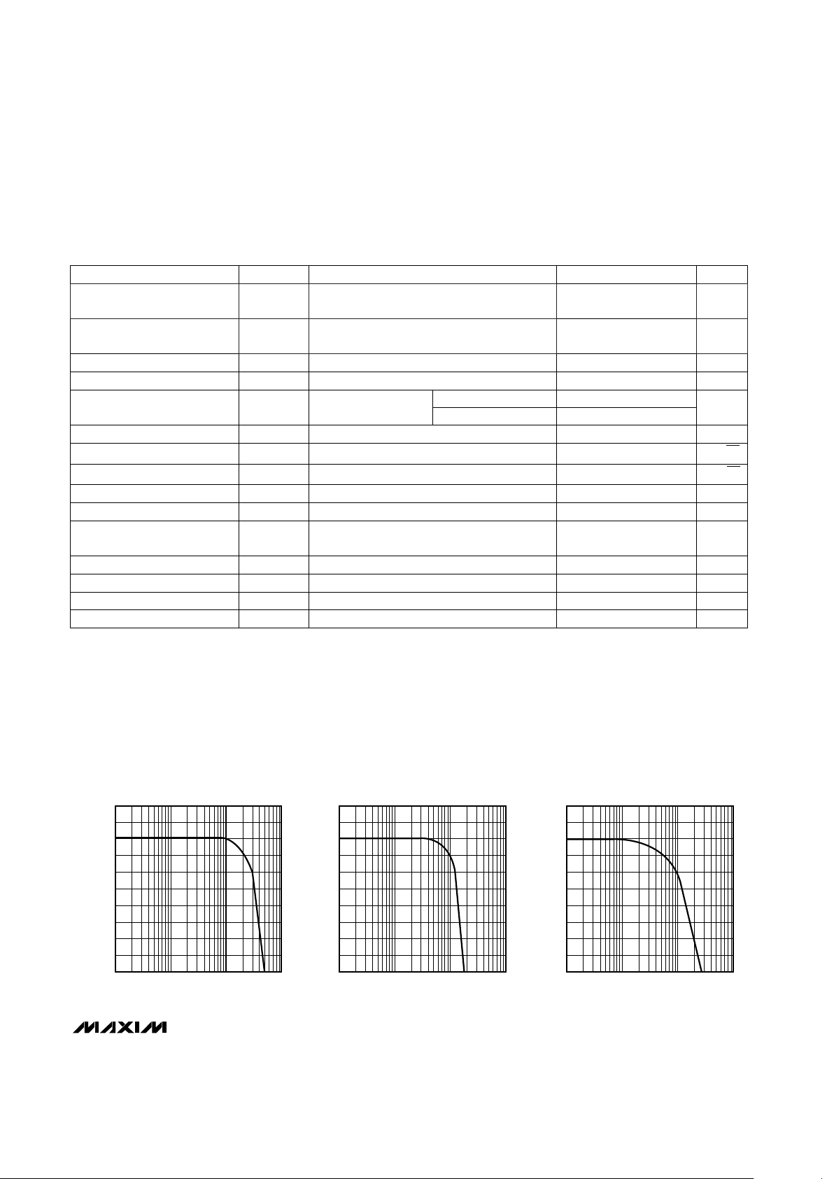
__________________________________________Typical Operating Characteristics
(VCC= +5V, VEE= -5V, RL= 100Ω, CL= 0pF, TA= +25°C, unless otherwise noted.)
1
2
0
-1
-2
1M 10M 100M 1G
SMALL-SIGNAL GAIN
vs. FREQUENCY (A
VCL
= +1V/V)
-6
-7
-8
-3
-4
-5
MAX477-01
FREQUENCY (Hz)
GAIN (dB)
6
7
8
5
4
3
1M 10M 100M 1G
SMALL-SIGNAL GAIN vs.
FREQUENCY (A
VCL
= +2V/V)
-1
-2
2
1
0
MAX477-02
FREQUENCY (Hz)
GAIN (dB)
20
21
22
19
18
17
100k 1M 10M 100M
SMALL-SIGNAL GAIN vs.
FREQUENCY (A
VCL
= +10V/V)
13
12
16
15
14
MAX477-03
FREQUENCY (Hz)
GAIN (dB)
V
OUT
≤ 0.1Vp-p MHzBW
-3dB
Small-Signal, -3dB Bandwidth
(Note 2)
BW
0.1dB
V
OUT
≤ 0.1Vp-p MHz
MAX477
300MHz High-Speed Op Amp
4 _______________________________________________________________________________________
____________________________Typical Operating Characteristics (continued)
(VCC= +5V, VEE= -5V, RL= 100Ω, CL= 0pF, TA= +25°C, unless otherwise noted.)
0
0.1
0.2
-0.1
-0.2
-0.3
1M 10M 100M 1G
GAIN FLATNESS
vs. FREQUENCY (A
VCL
= +1V/V)
-0.4
-0.5
-0.6
MAX477-04
FREQUENCY (Hz)
GAIN (dB)
1
2
3
0
-1
-2
1M 10M 100M 1G
LARGE-SIGNAL GAIN
vs. FREQUENCY (A
VCL
= +1V/V)
-3
-4
-5
-6
MAX477-05
FREQUENCY (Hz)
GAIN (dB)
SMALL-SIGNAL PULSE RESPONSE
(A
VCL
= +1V/V)
TIME (10ns/div)
VOLTAGE
(100mV/div)
GND
GND
IN
OUT
SMALL-SIGNAL PULSE RESPONSE
(A
VCL
= +2V/V)
TIME (10ns/div)
VOLTAGE
GND
GND
IN
(50mV/
div)
OUT
(100mV/
div)
LARGE-SIGNAL PULSE RESPONSE
(A
VCL
= +2V/V)
TIME (10ns/div)
VOLTAGE
GND
GND
IN
(1V/div)
OUT
(2V/div)
SMALL-SIGNAL PULSE RESPONSE
(A
VCL
= +10V/V)
TIME (50ns/div)
VOLTAGE
GND
GND
IN
(50mV/
div)
OUT
(500mV/
div)
LARGE-SIGNAL PULSE RESPONSE
(A
VCL
= +1V/V)
TIME (10ns/div)
VOLTAGE
(2V/div)
GND
GND
IN
OUT
LARGE-SIGNAL PULSE RESPONSE
(A
VCL
= +10V/V)
TIME (50ns/div)
VOLTAGE
GND
GND
IN
(200mV/
div)
OUT
(2V/div)
SMALL-SIGNAL PULSE RESPONSE
(A
VCL
= +1V/V, CL = 50pF)
TIME (20ns/div)
VOLTAGE
(100mV/div)
GND
GND
IN
OUT

MAX477
300MHz High-Speed Op Amp
_______________________________________________________________________________________
5
SMALL-SIGNAL PULSE RESPONSE
(A
VCL
= +1V/V, CL = 100pF)
TIME (20ns/div)
VOLTAGE
(100mV/div)
GND
GND
IN
OUT
LARGE-SIGNAL PULSE RESPONSE
(A
VCL
= +1V/V, CL = 50pF)
TIME (20ns/div)
VOLTAGE
(2V/div)
GND
GND
IN
OUT
LARGE-SIGNAL PULSE RESPONSE
(A
VCL
= +1V/V, CL = 100pF)
TIME (20ns/div)
VOLTAGE
(2V/div)
GND
GND
IN
OUT
-50
INPUT BIAS CURRENT (IB)
vs. TEMPERATURE
MAX477-19
TEMPERATURE (˚C)
INPUT BIAS CURRENT (µA)
0.5
0
1.0
1.5
2.0
2.5
3.0
3.5
-25 0 25 50 75 125100
V
CM
= 0V
-50
INPUT OFFSET VOLTAGE (VOS)
vs. TEMPERATURE
MAX477-17
TEMPERATURE (˚C)
INPUT OFFSET VOLTAGE (µV)
-200
-300
-100
0
100
200
300
400
-25 0 25 50 75 125100
VCM = 0V
-50
QUIESCENT SUPPLY CURRENT (ISY)
vs. TEMPERATURE
MAX477-18
TEMPERATURE (˚C)
QUIESCENT SUPPLY CURRENT (mA)
2
0
4
6
8
10
12
14
-25 0 25 50 75 125100
-50
OUTPUT VOLTAGE SWING
vs. TEMPERATURE
MAX477-20
TEMPERATURE (˚C)
OUTPUT VOLTAGE SWING (±V)
3.0
2.5
3.5
4.0
-25 0 25 50 75 125100
RL =
RL = 100Ω
RL = 50Ω
8
-50
INPUT COMMON-MODE RANGE (VCM)
vs. TEMPERATURE
MAX477-21
TEMPERATURE (˚C)
COMMON-MODE RANGE (±V)
3.2
3.8
3.6
3.4
3.0
2.8
4.0
4.2
-25 0 25 50 75 125100
____________________________Typical Operating Characteristics (continued)
(VCC= +5V, VEE= -5V, RL= 100Ω, CL= 0pF, TA= +25°C, unless otherwise noted.)
MAX477
300MHz High-Speed Op Amp
6 _______________________________________________________________________________________
____________________________Typical Operating Characteristics (continued)
(VCC= +5V, VEE= -5V, RL= 100Ω, CL= 0pF, TA= +25°C, unless otherwise noted.)
-30
-20
-110
-50
-70
-90
30k 100k 1M 10M 100M
POWER-SUPPLY REJECTION
vs. FREQUENCY
-100
MAX477-22
FREQUENCY (Hz)
POWER SUPPLY REJECTJION (dB)
-80
-60
-40
1k
0.1
100k 1M 10M 100M 500M
OUTPUT IMPEDANCE
vs. FREQUENCY
1
MAX477-23
FREQUENCY (Hz)
OUTPUT IMPEDANCE (Ω)
10
100
-20
-100
1k 10k 1M 10M100k 100M
HARMONIC DISTORTION
vs. FREQUENCY
-80
MAX477-24
FREQUENCY (Hz)
DISTORTION (dB)
-60
-40
TOTAL HARMONIC DISTORTION
SECOND HARMONIC
THIRD HARMONIC
50M
OPEN-LOOP
GAIN AND PHASE vs. FREQUENCY
MAX477-16
FREQUENCY (Hz)
OPEN-LOOP GAIN (dB)
PHASE (DEGREES)
-8
-10
-4
0
4
8
6
2
-2
-6
10
360
180
0
-180
-360
100M 500M
GAIN
PHASE
0.004
0.002
0.000
0.006
-0.004
0 100
0 100
DIFFERENTIAL GAIN AND PHASE
(A
VCL
= +1, RL = 150Ω)
0.000
-0.002
-0.002
-0.004
IRE
IRE
DIFF PHASE (deg)
DIFF GAIN (%)
0.006
0.004
0.002
MAX477-25
0.000
-0.004
0.004
0 100
0 100
DIFFERENTIAL GAIN AND PHASE
(A
VCL
= +2, RL = 150Ω)
0.000
-0.001
-0.002
-0.008
-0.012
IRE
IRE
DIFF PHASE (deg) DIFF GAIN (%)
0.003
0.002
0.001
MAX477-26

MAX477
300MHz High-Speed Op Amp
_______________________________________________________________________________________ 7
_______________Detailed Description
The MAX477 allows the flexibility and ease of a classic
voltage-feedback architecture while maintaining the
high-speed benefits of current-mode feedback (CMF)
amplifiers. Although the MAX477 is a voltage-feedback
op amp, its internal architecture provides an 1100V/µs
slew rate and a low 8mA supply current. CMF amplifiers offer high slew rates while maintaining low supply
current, but use the feedback and load resistors as part
of the amplifier’s frequency compensation network. In
addition, they have only one input with high impedance.
The MAX477 has speed and power specifications like
those of current-feedback amplifiers, but has high input
impedance at both input terminals. Like other voltagefeedback op amps, its frequency compensation is
independent of the feedback and load resistors, and it
exhibits a constant gain-bandwidth product. However,
unlike standard voltage-feedback amplifiers, its largesignal slew rate is not limited by an internal current
source, so the MAX477 exhibits a very high full-power
bandwidth.
Output Short-Circuit Protection
Under short-circuit conditions, the output current is typically limited to 150mA. This is low enough that a short to
ground of any duration will not cause permanent damage to the chip. However, a short to either supply will
significantly increase the power dissipation and may
cause permanent damage. The high outputcurrent capability is an advantage in systems that transmit a signal to several loads. See
High-Performance
Video Distribution Amplifier
in the
Applications
Information
section.
__________Applications Information
Grounding, Bypassing,
and PC Board Layout
To obtain the MAX477’s full 300MHz bandwidth, Microstrip and Stripline techniques are recommended in
most cases. To ensure the PC board does not degrade
the amplifier’s performance, design the board for a frequency greater than 1GHz. Even with very short traces,
use these techniques at critical points, such as inputs
and outputs. Whether you use a constant-impedance
board or not, observe the following guidelines when
designing the board:
• Do not use wire-wrap boards. They are too inductive.
• Do not use IC sockets. They increase parasitic
capacitance and inductance.
• In general, surface-mount components have shorter
leads and lower parasitic reactance, giving better
high-frequency performance than through-hole components.
• The PC board should have at least two layers, with
one side a signal layer and the other a ground plane.
• Keep signal lines as short and straight as possible.
Do not make 90° turns; round all corners.
• The ground plane should be as free from voids as
possible.
_____________________Pin Description
MAX477
V
OUT
= -(RF/RG) V
IN
V
OUT
V
IN
R
F
R
G
Figure 1a. Inverting Gain Configuration
MAX477
V
OUT
= [1 + (RF/RG)] V
IN
V
OUT
V
IN
R
F
R
G
Figure 1b. Noninverting Gain Configuration
Amplifier Output16
Positive Power
Supply
57
Negative Power
Supply
24
Noninverting Input33
PIN
SO/µMAX/DIP
Inverting Input42
No Connect. Not internally connected.
—1, 5, 8
FUNCTIONSOT23
OUT
V
CC
V
EE
IN+
IN-
N.C.
NAME

MAX477
300MHz High-Speed Op Amp
8 _______________________________________________________________________________________
Setting Gain
The MAX477 can be configured as an inverting or noninverting gain block in the same manner as any other
voltage-feedback op amp. The gain is determined by
the ratio of two resistors and does not affect amplifier
frequency compensation. This is unlike CMF op amps,
which have a limited range of feedback resistors, typically one resistor value for each gain and load setting.
This is because the -3dB bandwidth of a CMF op amp
is set by the feedback and load resistors. Figure 1a
shows the inverting gain configuration and its gain
equation, while Figure 1b shows the noninverting gain
configuration.
Choosing Resistor Values
The feedback and input resistor values are not critical
in the inverting or noninverting gain configurations (as
with current-feedback amplifiers). However, be sure to
select resistors that are small and noninductive.
Surface-mount resistors are best for high-frequency circuits. Their material is similar to that of metal-film resistors, but to minimize inductance, it is deposited in a flat,
linear manner using a thick film. Their small size and
lack of leads also minimize parasitic inductance and
capacitance.
The MAX477’s input capacitance is approximately 1pF.
In either the inverting or noninverting configuration,
excess phase resulting from the pole frequency formed
by Rf || Rgand C can degrade amplifier phase margin
and cause oscillations (Figure 2). Table 1 shows the
recommended resistor combinations and measured
bandwidth for several gain values.
DC and Noise Errors
The standard voltage-feedback topology of the
MAX477 allows DC error and noise calculations to be
done in the usual way. The following analysis shows
that the MAX477’s voltage-feedback architecture provides a precision amplifier with significantly lower DC
errors and lower noise compared to CMF amplifiers.
1) In Figure 3, total output offset error is given by:
For the special case in which R
S
is arranged to be
equal to R
f
|| Rg, the I
B
terms cancel out. Note also,
for IOS(RS+ (R
f
|| Rg) << V
OS
, the IOSterm also
drops out of the equation for total DC error. In practice, high-speed configurations for the MAX477
necessitate the use of low-value resistors for RS, Rf,
and Rg. In this case, the VOSterm is the dominant
DC error source.
2) The MAX477’s total input-referred noise in a closedloop feedback configuration can be calculated by:
where en= input-referred noise voltage of the
MAX477 (5nV√Hz)
in= input-referred noise current of the
MAX477 (2pA√Hz)
REQ= total equivalent source resistance at
the two inputs, i.e., REQ= RS+ R
f
|| R
g
eR =
resistor noise voltage due to REQ, i.e.,
MAX477
V
OUT
V
IN
C
R
F
R
G
R
L
Figure 2. Effect of High-Feedback Resistor Values and
Parasitic Capacitance on Bandwidth
Table 1. Resistor and Bandwidth Values for
Various Closed-Loop Gain Configurations
V = 1+
R
R
OUT
f
g
|| ||
+
( )
+ +
( )
( )
–V I R I R R I R R R
OS B S B f g OS S f g
e e e i R
T n R n EQ
= + +
( )
2 2
2
114
64
42
23
12
25
120
300
-3dB
BANDWIDTH
(MHz)
300
300
500
500
450
500
500
Short
R
f
(Ω)
300-1
150-2
100-5
50-10
50+10
125+5
GAIN
(V/V)
500+2
Open+1
R
g
(Ω)
e = 4KT R
R EQ

MAX477
300MHz High-Speed Op Amp
_______________________________________________________________________________________ 9
As an example, consider RS= 75Ω, Rf= Rg= 500Ω.
Then:
3) The MAX477’s output-referred noise is simply total
input-referred noise, eT, multiplied by the gain
factor:
In the above example, with eT= 5.5nV√Hz, and assuming a signal bandwidth of 300MHz (471MHz noise
bandwidth), total output noise in this bandwidth is:
Note that for both DC and noise calculations, errors are
dominated by offset voltage (VOS) and input noise voltage (en). For a current-mode feedback amplifier with
offset and noise errors significantly higher, the calculations are very different.
Driving Capacitive Loads
The MAX477 provides maximum AC performance with
no output load capacitance. This is the case when the
MAX477 is driving a correctly terminated transmission
line (i.e., a back-terminated 75Ω cable). However, the
MAX477 is capable of driving capacitive loads up to
100pF without oscillations, but with reduced AC performance.
Driving large capacitive loads increases the chance of
oscillations in most amplifier circuits. This is especially
true for circuits with high loop gain, such as voltage followers. The amplifier’s output resistance and the load
capacitor combine to add a pole and excess phase to
the loop response. If the frequency of this pole is low
enough and phase margin is degraded sufficiently,
oscillations may occur.
A second problem when driving capacitive loads
results from the amplifier’s output impedance, which
looks inductive at high frequency. This inductance
forms an L-C resonant circuit with the capacitive load,
which causes peaking in the frequency response and
degrades the amplifier’s gain margin.
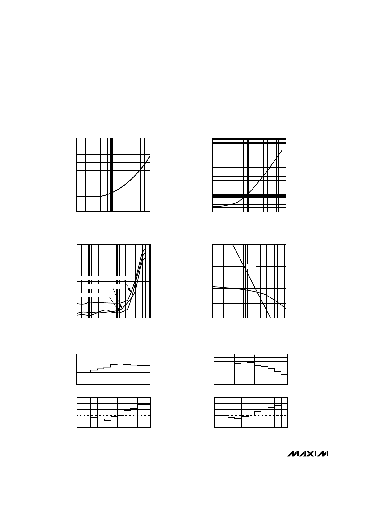
The MAX477 drives capacitive loads up to 100pF without oscillation. However, some peaking (in the frequency domain) or ringing (in the time domain) may occur.
This is shown in Figure 4 and the in the Small and
Large-Signal Pulse Response graphs in the
Typical
Operating Characteristics
.
To drive larger-capacitance loads or to reduce ringing,
add an isolation resistor between the amplifier’s output
and the load, as shown in Figure 5.
The value of R
ISO
depends on the circuit’s gain and the
capacitive load. Figure 6 shows the Bode plots that
result when a 20Ω isolation resistor is used with a voltage follower driving a range of capacitive loads. At the
higher capacitor values, the bandwidth is dominated by
the RC network, formed by R
ISO
and CL; the bandwidth
of the amplifier itself is much higher. Note that adding
an isolation resistor degrades gain accuracy. The load
and isolation resistor form a divider that decreases the
voltage delivered to the load.
R
e KT x nV Hz at C
e nV nV pA x nV Hz
EQ
R
T
= +
( )
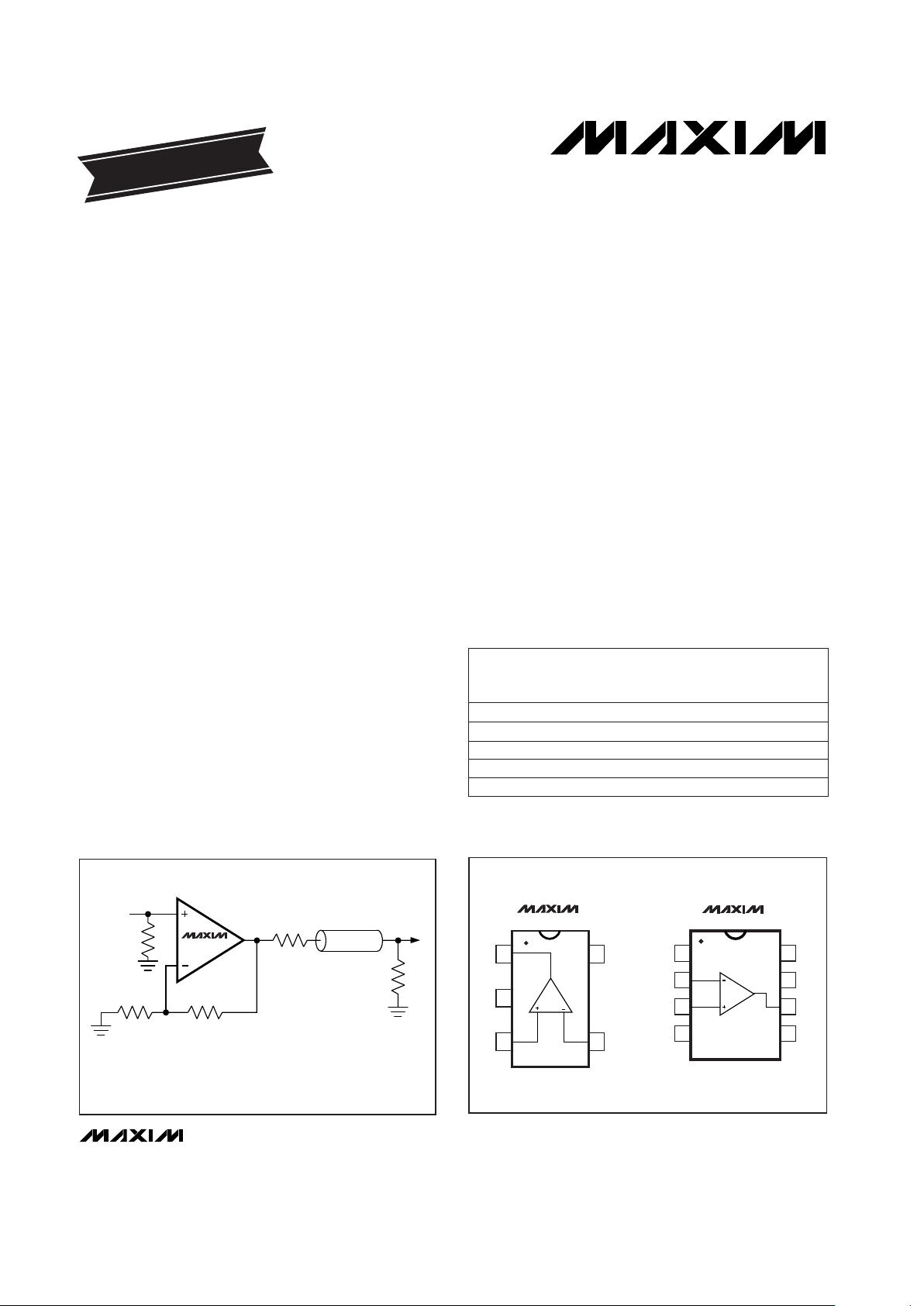
=
= = °
=
( )+( )+( )
=
75 500 500 325
4 325 2 3 25
5 2 3 2 325 5 5
2 2 2
Ω Ω Ω Ω
. /
. .
||
e = 5.5nV x
OUT
1
500
500
471 239+
= x MHz V
RMS
µ
e = e 1+
R
R
OUT T
f
g
MAX477
V
OUT
I
B-
I
B+
R
f
R
g
R
S
V
IN
Figure 3. Output Offset Voltage
Figure 4. Effect of C
LOAD
on Frequency Response
(A
VCL
= +1V/V)
15
10
5
0
1M 10M 100M 1G
-20
-5
-10
-15
FREQUENCY (Hz)
GAIN (dB)
CL = 100pF
C
L
= 22pF
C
L
= 41pF
CL = 0pF

MAX477
300MHz High-Speed Op Amp
10 ______________________________________________________________________________________
Flash ADC Preamp
The MAX477’s high output-drive capability and ability
to drive capacitive loads make it well suited for buffering the low-impedance input of a high-speed flash
ADC. With its low output impedance, the MAX477 can
drive the inputs of the ADC while maintaining accuracy.
Figure 7 shows a preamp for digitizing video, using the
250Msps MAX100 and the 500Msps MAX101 flash
ADCs. Both of these ADCs have a 50Ω input resistance
and a 1.2GHz input bandwidth.
High-Performance Video
Distribution Amplifier
In a gain of +2 configuration, the MAX477 makes an
excellent driver for back-terminated 75Ω video coaxial
cables (Figure 8). The high output-current drive allows
the attachment of up to six ±2Vp-p, 150Ω loads to the
MAX477 at +25°C. With the output limited to ±1Vp-p,
the number of loads may double. The MAX4278 is a
similar amplifier configured for a gain of +2 without the
need for external gain-setting resistors. For multiple
gain-of-2 video line drivers in a single package, see the
MAX496/MAX497 data sheet.
Wide-Bandwidth Bessel Filter
Two high-impedance inputs allow the MAX477 to be
used in all standard active filter topologies. The filter
design is straightforward because the component values can be chosen independently of op amp bias.
Figure 9 shows a wide-bandwidth, second-order Bessel
filter using a multiple feedback topology. The component values are chosen for a gain of +2, a -3dB bandwidth of 10MHz, and a 28ns delay. Figure 10a shows a
square-wave pulse response, and Figure 10b shows the
filter’s frequency response and delay. Notice the flat
delay in the passband, which is characteristic of the
Bessel filter.
MAX477
V
OUT
V
IN
R
ISO
C
L
R
L
Figure 5. Capacitive-Load Driving Circuit
MAX477
VIDEO IN
75Ω
500Ω500Ω
75Ω
75Ω
75Ω
75Ω
75Ω
75Ω
75Ω
75Ω
OUT1
OUT2
OUTN
Figure 8. High-Performance Video Distribution Amplifier
MAX477
VIDEO IN
500Ω 500Ω
FLASH ADC
(MAX100/MAX101)
Figure 7. Preamp for Video Digitizer
Figure 6. Effect of C
LOAD
on Frequency Response With
Isolation Resistor
1
0
-1
-2
1M 10M 100M 1G
-6
-3
-4
-5
FREQUENCY (Hz)
GAIN (dB)
CL = 0pF
R
ISO
= 20Ω
C
L
= 22pF
CL = 47pF
CL = 100pF

MAX477
300MHz High-Speed Op Amp
______________________________________________________________________________________ 11
MAX477
V
OUT
V
IN
20pF
100pF
602Ω
110Ω301Ω
Figure 9. 8MHz Bessel Filter
Figure 10a. 5MHz Square Wave Input
TIME (50ns/div)
VOLTAGE (V)
GND
GND
IN
(100mV/div)
-0.2V
OUT
(200mV/div)
0.2V
Figure 10b. Gain and Delay vs. Frequency
1M 10M 100M
FREQUENCY (MHz)
GAIN (dB)
DELAY (ns)
-8
0
4
-4
38
48
18
8
28
-2
-12
-22
-32
-42
-52
8
10
6
2
-2
-6
-10
DELAY
GAIN
___________________Chip Information
TRANSISTOR COUNT: 175
SUBSTRATE CONNECTED TO V
EE

MAX477
300MHz High-Speed Op Amp
12 ______________________________________________________________________________________
________________________________________________________Package Information
SOT5L.EPS
8LUMAXD.EPS
 Loading...