

General Description
The MAX4762–MAX4764/MAX4764A/MAX4765 dual
SPDT (single-pole/double-throw) switches feature negative signal capability that allows signals below ground to
pass through without distortion. These analog switches
operate from a single +1.8V to +5.5V supply and have
low 0.6Ω on-resistance, making them ideal for switching
audio signals.
The MAX4763/MAX4765 include a comparator that can
be used for headphone detection or a mute/send key
function. The MAX4764/MAX4764A/MAX4765 have an
internal shunt switch to automatically discharge any
capacitance at the NO and NC connection points. This
reduces click-and-pop sounds that occur when switching
audio signals between precharged points.
These SPDT switches are available in space-saving
µMAX®, TDFN, thin QFN, and UCSP™packages and
operate over the -40°C to +85°C extended temperature range.
Applications
Cell Phones
PDAs and Handheld Devices
Notebook Computers
MP3 Players
Features
♦ Distortion-Free Negative Signal Throughput Down
to VCC- 5.5V
♦ Comparator for Headphone or Mute Detection
(MAX4763/MAX4765)
♦ Internal Shunt Resistor Reduces Click/Pop
(MAX4764/MAX4764A/MAX4765)
♦ Low On-Resistance (R
ON
)
0.6Ω at +2.7V Supply
♦ 0.25Ω On-Resistance Flatness
♦ 0.05Ω On-Resistance Matching
♦ +1.8V to +5.5V Supply Voltage
♦ -70dB Crosstalk (100kHz)
♦ -65dB Off-Isolation (100kHz)
♦ 0.01% Total Harmonic Distortion
♦ Available in µMAX, TDFN, Thin QFN, and UCSP
Packages
MAX4762–MAX4764/MAX4764A/MAX4765
Low-Voltage, Dual SPDT, Audio Clickless
Switches with Negative Rail Capability
________________________________________________________________ Maxim Integrated Products 1
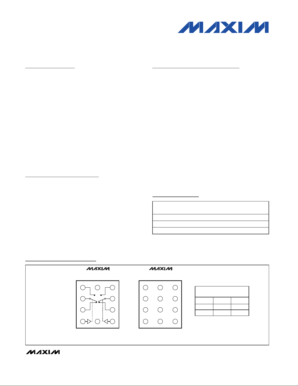
NC1NC2
IN1IN2
NO1
COM1COM2
NO2 V
CC
GND
TOP VIEW
IN_
0
1
NO_
MAX4762–MAX4764/
MAX4764A/MAX4765
OFF
ON
NC_
ON
SWITCHES SHOWN FOR LOGIC "0" INPUT
OFF
UCSP
MAX4762/MAX4764
C1
C2
C3
C4 B4 A4
A3
A2
A1B1
UCSP
MAX4763/MAX4765
C1
C2
C3
C4 B4 A4
A3
A2
A1B1
(BUMP SIDE DOWN)
B2
B3
NO2 V
CC
NO1
COM2 COM1
NC1CMP-NC2
IN2 GND IN1
CMPO
Pin Configurations/Functional Diagrams/Truth Table
Ordering Information
19-3152; Rev 2; 1/06
For pricing, delivery, and ordering information, please contact Maxim/Dallas Direct! at
1-888-629-4642, or visit Maxim’s website at www.maxim-ic.com.
Pin Configurations/Functional Diagrams/Truth Table continued at end of data sheet.
PART
TEMP RANGE
PINPACKAGE
TOP
MARK
MAX4762ETB
10 TDFN
ACG
MAX4762EUB
10 µMAX —
MAX4762EBC-T
12 UCSP-12
ABU
Ordering Information continued at end of data sheet.
Selector Guide appears at end of data sheet.
µMAX is a registered trademark and UCSP is a trademark of
Maxim Integrated Products, Inc.
-40°C to +85°C
-40°C to +85°C
-40°C to +85°C
MAX4762–MAX4764/MAX4764A/MAX4765
Low-Voltage, Dual SPDT, Audio Clickless
Switches with Negative Rail Capability
2 _______________________________________________________________________________________
ABSOLUTE MAXIMUM RATINGS
ELECTRICAL CHARACTERISTICS
(VCC= +2.7V to +5.5V, TA= -40°C to +85°C, unless otherwise noted. Typical values are at VCC= +3.0V, TA= +25°C, unless otherwise
noted.) (Note 1)
Stresses beyond those listed under “Absolute Maximum Ratings” may cause permanent damage to the device. These are stress ratings only, and functional
operation of the device at these or any other conditions beyond those indicated in the operational sections of the specifications is not implied. Exposure to
absolute maximum rating conditions for extended periods may affect device reliability.
(All voltages referenced to GND.)
V
CC
, IN_, CMP-......................................................-0.3V to +6.0V
COM_, NO_, NC_ ...............................(V
CC
- 6V) to (VCC+ 0.3V)
CMPO .........................................................-0.3V to (V
CC
+ 0.3V)
Closed-Switch Continuous Current COM_, NO_, NC_......±150mA
Open-Switch Continuous Current NO_, NC_
(MAX4764/MAX4764A/MAX4765) ................................±30mA
Peak Current COM_, NO_, NC_
(pulsed at 1ms, 50% duty cycle)................................±300mA
Peak Current COM_, NO_, NC_
(pulsed at 1ms, 10% duty cycle)................................±400mA
Continuous Power Dissipation (T
A
= +70°C)
10-Pin TDFN (derate 24.4mW/°C above +70°C) .......1951mW
10-Pin µMAX (derate 5.6mW/°C above +70°C) ...........444mW
12-Bump UCSP (MAX4762/MAX4764)
(derate 5.6mW/°C above +70°C).............................449mW
12-Bump UCSP (MAX4763/MAX4765)
(derate 6.5mW/°C above +70°C).............................519mW
12-Pin Thin QFN (derate 16.9mW/°C above +70°C) ....1349mW
ESD Method 3015.7 .............................................................±2kV
Operating Temperature Range ...........................-40°C to +85°C
Junction Temperature......................................................+150°C
Storage Temperature Range .............................-65°C to +150°C
Lead Temperature (soldering, 10s) .................................+300°C
Bump Temperature (soldering)
Infrared (15s) ...............................................................+220°C
Vapor Phase (60s) .......................................................+215°C
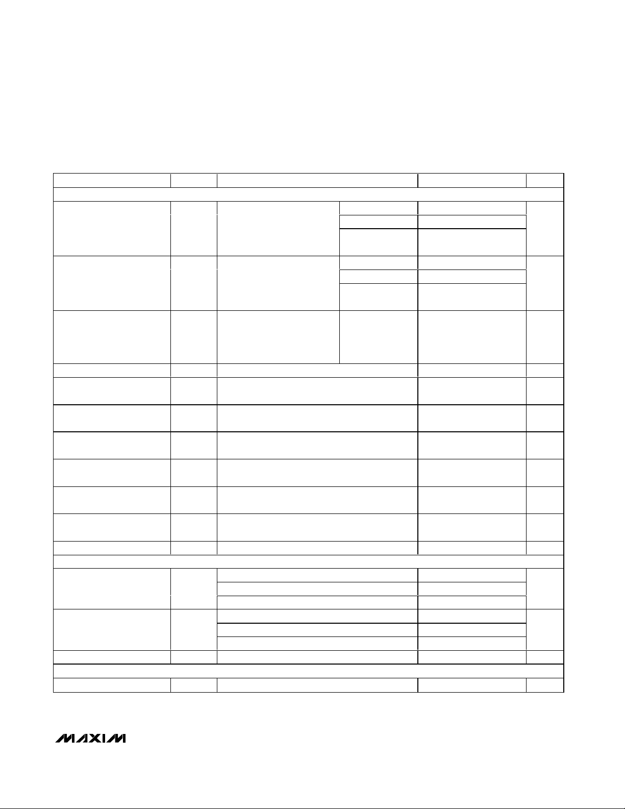
PARAMETER
CONDITIONS
UNITS
ANALOG SWITCH
Analog Signal Range
(Note 2)
V
NO_
,
V
NC_
,
VCC -
5.5
V
0.6
On-Resistance
(Notes 3 and 4)
),
)
VCC = 2.7V; V
NC_
or V
NO_
=
V
CC
- 5.5V, -1V, 0V, 1V, 2V, VCC;
I
COM_
= 100mA
T
A
= T
MIN
to T
MAX
Ω
0.1
On-Resistance Match
Between Channels
(Notes 3, 4, and 5)
∆R
ON
VCC = 2.7V, V
NC_
or V
NO_
= 0V,
I
COM
= 100mA
T
A
= T
MIN
to T
MAX
Ω
0.4
On-Resistance Flatness
(Notes 4 and 6)
)
VCC = 2.7V; V
NC_
or VNC =
-1V, 0V, 1V, 2V, V
CC
;
I
COM_
= 100mA
T
A
= T
MIN
to T
MAX
Ω
Shunt Switch Resistance R
SH
I
NO_
or I
NC_
= 10mA, VCC = 2.7V
T
A
= T
MIN
to T
MAX
25 50 Ω
-2 +2
NO_, NC_
Off-Leakage Current
(Notes 8 and 9)
),
)
MAX4762/MAX4763 only (Note 7),
V
CC
= 2.7V, switch open;
V
NC_
or V
NO_
= -2.5V, +2.5V;
V
COM_
= +2.5V, -2.5V
TA = T
MIN
to T
MAX
-10
nA
-6 +6
COM_ On-Leakage Current
(Notes 8 and 9)
)
VCC = 2.7V, switch closed;
V
NC_
or V
NO_
= -2.5V, +2.5V, or
floating; V
COM_
= -2.5V, +2.5V, or
floating
T
A
= T
MIN
to T
MAX
-50
nA
SYMBOL
MIN TYP MAX
V
COM_
TA = +25°C
R
ON(NC
R
ON(NO
TA = +25°C 0.05
R
FLAT(NC
I
NO_(OFF
I
NC_(OFF
I
COM_(ON
MAX4764/MAX4764A/MAX4765 only,
TA = +25°C 0.25
TA = +25°C
TA = +25°C
V
CC
0.85
0.95
0.15
0.45
+10
+50
MAX4762–MAX4764/MAX4764A/MAX4765
Low-Voltage, Dual SPDT, Audio Clickless
Switches with Negative Rail Capability
_______________________________________________________________________________________ 3
ELECTRICAL CHARACTERISTICS (continued)
(VCC= +2.7V to +5.5V, TA= -40°C to +85°C, unless otherwise noted. Typical values are at VCC= +3.0V, TA= +25°C, unless otherwise
noted.) (Note 1)
PARAMETER
CONDITIONS
UNITS
DYNAMIC CHARACTERISTICS
TA = +25°C 25 80
80
Turn-On Time t
ON
VCC = 2.7V, VNO = 1.5V; for
NO_, V
IN_
= 0V to VCC; for
NC_, V
IN_
= VCC to 0V; RL =
300Ω, C
L
= 35pF, Figure 2
T
A
= T
MIN
to T
MAX
(MAX4764A)
500
ns
TA = +25°C 20 70
70
Turn-Off Time t
OFF
VCC = 2.7V, VNC = 1.5V; for
NO_, V
IN_
= VCC to 0V; for
NC_, V
IN_
= 0V to VCC; RL =
300Ω, C
L
= 35pF, Figure 2
T
A
= T
MIN
to T
MAX
(MAX4764A)
500
ns
Break-Before-Make
Time Delay
t
D
VCC = 2.7V, VN_ = 1.5V, for
NO_, V
IN_
= VCC to 0V; for
NC_, V
IN_
= 0V to VCC; RL =
300Ω, C
L
= 35pF, Figure 3
T
A
= +25°C 1 7 ns
Charge Injection Q V
COM_
= 0V, CL = 1.0nF, Figure 4
pC
Off-Isolation (Note 10) V
ISO
f = 100kHz, V
COM_
= 1V
RMS
, RL = 50Ω, CL = 5pF,
Figure 5
-65 dB
Crosstalk V
CT
f = 100kHz, V
COM_
= 1V
RMS
, RL = 50Ω, CL = 5pF,
Figure 5
-70 dB
Power-Supply Rejection
Ratio
PSRR f = 10kHz, V
COM_
= 1V
RMS
, RL = 50Ω, CL = 5pF 60 dB
On-Channel -3dB
Bandwidth
BW Signal = 0dBm, R
L
= 50Ω, CL = 5pF, Figure 5 27
MHz
Total Harmonic Distortion THD
f = 20Hz to 20kHz, V
COM_
= 0.5V
P-P
, DC Bias = 0,
R
L
= 32Ω
%
NO_, NC_ Off-Capacitance
)
)
50 pF
COM On-Capacitance
)
pF
DIGITAL I/O (IN_)
VCC = 2.7V to 3.6V 1.4
VCC = 4.2V to 5.5V 2.0Input-Logic High Voltage V
IH
VCC = 2.7V to 5.5V (MAX4764A only) 1.6
V
VCC = 2.7V to 3.6V 0.5
VCC = 4.2V to 5.5V 0.8Input-Logic Low Voltage V
IL
VCC = 2.7V to 5.5V (MAX4764A only) 0.5
V
Input Leakage Current I
IN
V
IN_
= 0V or V
CC
-1 +1 µA
COMPARATOR (MAX4763/MAX4765)
Comparator Threshold
V
SYMBOL
C
NO_(OFF
C
NC_(OFF
C
COM_(ON
f = 1MHz, V
f = 1MHz, V
MIN TYP MAX
TA = T
MIN
to T
MAX
225
TA = T
MIN
to T
MAX
225
150
= 0.5V
COM_
= 0.5V
COM_
, DC Bias = 0, Figure 6
P-P
, DC Bias = 0, Figure 6 200
P-P
0.01
VCC / 3

MAX4762–MAX4764/MAX4764A/MAX4765
Low-Voltage, Dual SPDT, Audio Clickless
Switches with Negative Rail Capability
4 _______________________________________________________________________________________
ELECTRICAL CHARACTERISTICS (continued)
(VCC= +2.7V to +5.5V, TA= -40°C to +85°C, unless otherwise noted. Typical values are at VCC= +3.0V, TA= +25°C, unless otherwise
noted.) (Note 1)
PARAMETER
SYMBOL
CONDITIONS
MIN
TYP
MAX
UNITS
Comparator Output High
Voltage
I
SOURCE
= 1mA
V
CC
V
Comparator Output Low
Voltage
I
SINK
= 1mA
V
Comparator Input Leakage
Current
V
CMP-
= 0 to 2.7V
nA
Comparator Switching Time
VCC = 2.7V, V
CMP-
= 0V to VCC,
from 50% of V
CMP-
to 50% of V
CMPO
12µs
POWER SUPPLY
Power-Supply Range V
CC
1.8 5.5 V
510
VCC = 5.5V, V
IN_
= 0V or
V
CC
MAX4762/MAX4764/
MAX4764A
1
VCC = 5.5V, V
IN_
= 1.8V MAX4764A 5 10
Supply Current I+
V
CC
= 4.2V, V
IN_
= 1.8V
(Note 11)
MAX4764A 2 5
µA
Note 1: UCSP and TDFN parts are 100% tested at TA= +25°C only, and guaranteed by design over the specified temperature range.
Thin QFN parts are 100% tested at T
A
= +85°C only, and guaranteed by design over the specified temperature range.
Note 2: Signals on COM_, NO_, or NC_ exceeding V
CC
are clamped by internal diodes. Limit forward-diode current to maximum
current rating.
Note 3: Thin QFN and UCSP are guaranteed by design; not production tested.
Note 4: I
COM
for UCSP is 10mA.
Note 5: ∆R
ON
= R
ON(MAX)
- R
ON(MIN).
Note 6: Flatness is defined as the difference between the maximum and minimum value of on-resistance as measured over the
specified analog signal ranges.
Note 7: MAX4764/MAX4764A/MAX4765 have an internal shunt switch when in off-state, which determines OFF current.
Note 8: Leakage parameters are 100% tested at maximum-rated hot operating temperature and guaranteed by design at T
A
= +25°C.
Note 9: UCSP parts are guaranteed by design.
Note 10: Off-isolation = 20log
10(VCOM
/ VNO), V
COM
= output, VNO= input to off switch.
Note 11: Guaranteed by design, not production tested.
0.4V
0.4V
-100 +100
MAX4763/MAX4765
0.01
MAX4762–MAX4764/MAX4764A/MAX4765
Low-Voltage, Dual SPDT, Audio Clickless
Switches with Negative Rail Capability
_______________________________________________________________________________________ 5
ON-RESISTANCE vs. COM VOLTAGE
MAX4762 toc01
COM VOLTAGE (V)
ON-RESISTANCE (Ω)
43210-1-2-3
1
2
3
4
5
6
0
-4 5
VCC = 1.8V
VCC = 2.0V
VCC = 2.3V
V+ = 2.5V
V+ = 3.0V
V+ = 5.0V
ON-RESISTANCE vs. COM VOLTAGE
MAX4762 toc02
COM VOLTAGE (V)
ON-RESISTANCE (Ω)
43210
0.2
0.4
0.6
0.8
1.0
1.2
0
-1 5
VCC = 5.0V
TA = +85°C
TA = +25°C
TA = -40°C
ON-RESISTANCE vs. COM VOLTAGE
MAX4762 toc03
COM VOLTAGE (V)
ON-RESISTANCE (Ω)
210-1-2
0.2
0.4
0.6
0.8
1.0
1.2
0
-3 3
VCC = 3.0V
TA = +85°C
TA = +25°C
TA = -40°C
MAX4762/MAX4764/MAX4764A
SUPPLY CURRENT vs. SUPPLY VOLTAGE
MAX4762 toc04
SUPPLY VOLTAGE (V)
SUPPLY CURRENT (nA)
5.34.84.33.83.32.82.3
20
40
60
80
100
0
1.8
MAX4763/MAX4765
SUPPLY CURRENT vs. SUPPLY VOLTAGE
MAX4762 toc05
SUPPLY VOLTAGE (V)
SUPPLY CURRENT (nA)
5.34.84.33.83.32.82.31.8
1
2
3
4
5
6
0
MAX4762–MAX4765
TURN-ON/TURN-OFF TIME
vs. SUPPLY VOLTAGE
MAX4762 toc06
SUPPLY VOLTAGE (V)
t
ON
/t
OFF
(ns)
5.34.84.33.83.32.82.31.8
10
20
30
40
50
60
70
0
t
ON
t
OFF
MAX4762–MAX4765
TURN-ON/TURN-OFF TIME
vs. TEMPERATURE
MAX4762 toc07
TEMPERATURE (°C)
t
ON
/t
OFF
(ns)
603510-15
10
20
30
40
0
-40 85
t
ON
t
OFF
V
CC
= 3.0V
MAX4762–MAX4765
LOGIC THRESHOLD vs. SUPPLY VOLTAGE
MAX4762 toc08
SUPPLY VOLTAGE (V)
LOGIC THRESHOLD (V)
5.34.84.33.83.32.82.3
0.4
0.8
1.2
1.6
2.0
0
1.8
VIN RISING
VIN FALLING
-200
-100
100
0
200
300
-3 -1 0-2 12345
CHARGE INJECTION
vs. V
COM
MAX4762 toc09
V
COM
(V)
CHARGE INJECTION (pC)
CL = 1nF
VCC = 5.0V
VCC = 2.0V
Typical Operating Characteristics
(VCC= 3.0V, TA = +25°C, unless otherwise noted.)

MAX4762–MAX4764/MAX4764A/MAX4765
Low-Voltage, Dual SPDT, Audio Clickless
Switches with Negative Rail Capability
6 _______________________________________________________________________________________
Typical Operating Characteristics (continued)
(VCC= 3.0V, TA = +25°C, unless otherwise noted.)
LEAKAGE CURRENT vs. TEMPERATURE
MAX4762 toc10
TEMPERATURE (°C)
LEAKAGE CURRENT (pA)
603510-15
10
100
1000
1
-40 85
VCC = 3.0V
I
COM(ON)
I
COM(OFF)
0
0.001 0.01 0.1 1 10 100
-3
-9
-12
-6
-15
-18
FREQUENCY RESPONSE
vs. ON-LOSS
MAX4762 toc11
FREQUENCY (MHz)
ON-LOSS (dB)
VCC = 3.0V
0
0.001 0.01 0.1 1 10 100
-20
-60
-80
-40
-100
-120
FREQUENCY RESPONSE
OFF-ISOLATION, CROSSTALK
MAX4762 toc12
FREQUENCY (MHz)
ON-LOSS (dB)
VCC = 3.0V
OFF-ISOLATION
CROSSTALK
10 1k
100 10k
100k
TOTAL HARMONIC DISTORTION
vs. FREQUENCY
FREQUENCY (Hz)
THD (%)
1
0.01
0.1
MAX4762 toc13
VCC = 3.0V
R
L
= 32Ω
0
20
60
40
80
100
POWER-SUPPLY REJECTION RATIO
vs. FREQUENCY
MAX4762 toc14
FREQUENCY (Hz)
PSRR (dB)
100 10k1k 100k 1M
VCC = 1V
RMS
DC BIAS = 3V
C
L
= 5pF
R
L
= 50Ω
COMPARATOR THRESHOLD
vs. TEMPERATURE
MAX4762 toc15
TEMPERATURE (°C)
COMPARATOR THRESHOLD (V)
603510-15
1.60
1.65
1.70
1.75
1.55
-40 85
VCC = 5.0V
V
CMP-
RISING
V
CMP-
FALLING
COMPARATOR THRESHOLD
vs. TEMPERATURE
MAX4762 toc16
TEMPERATURE (°C)
COMPARATOR THRESHOLD (V)
603510-15-40 85
VCC = 3.0V
V
CMP-
RISING
V
CMP-
FALLING
0.94
0.96
0.98
1.00
1.02
0.92

MAX4762–MAX4764/MAX4764A/MAX4765
Low-Voltage, Dual SPDT, Audio Clickless
Switches with Negative Rail Capability
_______________________________________________________________________________________ 7
Pin Description (MAX4762/MAX4764/MAX4764A)
PIN
10-µMAX
10-TDFN
NAME FUNCTION
1B1VCCPositive-Supply Voltage Input
2A1NO1 Analog Switch 1—Normally Open Terminal
3A2COM1 Analog Switch 1—Common Terminal
4A3NC1 Analog Switch 1—Normally Closed Terminal
5A4IN1
Digital Control Input for Analog Switch 1. A logic LOW on IN1 connects COM1 to NC1 and
a logic HIGH connects COM1 to NO1.
6B4GND Ground
7C4IN2
Digital Control Input for Analog Switch 2. A logic LOW on IN2 connects COM2 to NC2 and
a logic HIGH connects COM2 to NO2.
8C3NC2 Analog Switch 2—Normally Closed Terminal
9C2COM2 Analog Switch 2—Common Terminal
10 C1 NO2 Analog Switch 2—Normally Open Terminal
EP (TDFN
only)
—EPExposed pad for TDFN package. Connect to GND.
Pin Description (MAX4763/MAX4765)
PIN
12-Thin
QFN
NAME FUNCTION
1A2COM1 Analog Switch 1—Common Terminal
2A3NC1 Analog Switch 1—Normally Closed Terminal
3A4IN1
Digital Control Input for Analog Switch 1. A logic LOW on IN1 connects COM1 to NC1
and a logic HIGH connects COM1 to NO1.
4B3CMP- Comparator Inverting Input
5B4GND Ground
6C4IN2
Digital Control Input for Analog Switch 2. A logic LOW on IN2 connects COM2 to NC2
and a logic HIGH connects COM2 to NO2.
7C3NC2 Analog Switch 2—Normally Closed Terminal
8C2COM2 Analog Switch 2—Common Terminal
9C1NO2 Analog Switch 2—Normally Open Terminal
10 B2 CMPO Comparator Output
11 B1 V
CC
Positive-Supply Voltage Input
12 A1 NO1 Analog Switch 1—Normally Open Terminal
EP — EP Exposed pad. Connect to GND.
12-UCSP
12-UCSP

MAX4762–MAX4764/MAX4764A/MAX4765
Detailed Description
The MAX4762–MAX4764/MAX4764A/MAX4765 are low
on-resistance, low-voltage, dual SPDT analog switches
that operate from a +1.8V to +5.5V supply and are fully
specified for nominal 3.0V applications. The devices
feature a negative signal capability that allows signals
below ground to pass through without distortion and
have break-before-make switching.
The MAX4763/MAX4765 feature a comparator that can be
used for headphone or mute detection. The comparator
threshold is internally generated to be approximately 1/3
of VCC. The MAX4764/MAX4764A/MAX4765 feature an
internal shunt switch to discharge any capacitance at the
NO and NC connection points. This reduces the clickand-pop sounds that occur when switching audio signals.
Applications Information
Digital Control Inputs
The MAX4762–MAX4764/MAX4764A/MAX4765 logic
inputs accept up to +5.5V, regardless of supply voltage.
For example, with a +3.3V supply, IN_ can be driven low
to GND and high to +5.5V allowing for mixing of logic
levels in a system. Driving IN_ rail-to-rail minimizes
power consumption. For a +1.8V supply voltage, the
logic thresholds are 0.5V (low) and 1.4V (high); for a
+5V supply voltage, the logic thresholds are 0.8V (low)
and 2.0V (high).
Analog Signal Levels
The on-resistance of the MAX4762–MAX4764/
MAX4764A/MAX4765 changes very little for analog input
signals across the entire supply voltage range (see the
Typical Operating Characteristics). The switches are bidirectional, so the NO_, NC_, and COM_ pins can be either
inputs or outputs.
The MAX4762–MAX4764/MAX4764A/MAX4765 pass
signals as low as VCC- 5.5V, including signals below
ground with minimal distortion.
Comparator (MAX4763/MAX4765)
The MAX4763/MAX4765 include a comparator that can
be used for mute and headphone detection functions.
The positive terminal of the comparator is internally set to
V
CC
/ 3. When the negative terminal (CMP-) is below the
threshold, the comparator output (CMPO) is a logic high.
When CMP- rises above V
CC
/ 3, CMPO is a logic low.
The comparator threshold of V
CC
/ 3 allows for detection
of headphones because headphone audio signals are
typically biased to V
CC
/ 2.
Shunt Switch
(MAX4764/MAX4764A/MAX4765)
The 100Ω shunt switches on the MAX4764/MAX4764A/
MAX4765 automatically discharge any capacitance at
the NC_ or NO_ terminals when they are unconnected
to COM_. This reduces audible click-and-pop sounds
that occur when switching between audio sources.
Audible clicks and pops are caused when a step DC
voltage is switched into the speaker. By automatically
discharging the side that is not connected, any residual
DC voltage is removed, thereby reducing the clicks
and pops.
Power-Supply Sequencing and
Overvoltage Protection
Caution: Do not exceed the absolute maximum ratings
since stresses beyond the listed ratings may cause
permanent damage to the device.
Proper power-supply sequencing is recommended for
all CMOS devices. Always apply VCCbefore applying
analog signals, especially if the analog signal is not
current-limited.
UCSP Applications Information
For the latest application details on UCSP construction,
dimensions, tape carrier information, printed circuit board
techniques, bump-pad layout, and recommended reflow
temperature profile, as well as the latest information on
reliability testing results, go to the Maxim’s website at
www.maxim-ic.com/ucsp and search for the Application
Note, “UCSP—A Wafer-Level Chip-Scale Package.”
Low-Voltage, Dual SPDT, Audio Clickless
Switches with Negative Rail Capability
8 _______________________________________________________________________________________
AUDIO
SOURCE 1
AUDIO
SOURCE 2
V+
3
MUTE
BUTTON
V+
MAX4765
OUT+
OUT-
OUT+
OUT-
NC1
NO1
NC2
NO2
CMPO
COM1
IN1
IN2
COM2
CMP-
8Ω
SPEAKER
INPUT
SELECT
MUTE
SHUNT
SWITCH
Figure 1. Typical Operating Circuit

MAX4762–MAX4764/MAX4764A/MAX4765
Low-Voltage, Dual SPDT, Audio Clickless
Switches with Negative Rail Capability
_______________________________________________________________________________________ 9
Test Circuits/Timing Diagrams
tr < 5ns
tf < 5ns
50%
0V
LOGIC
INPUT
R
L
COM_
GND
IN_
C
L
INCLUDES FIXTURE AND STRAY CAPACITANCE.
V
OUT
= V
N_ (
R
L
)
RL + R
ON
V
N_
V
CC
t
OFF
0V
NO_
OR NC_
0.9 x V
0UT
0.9 x V
OUT
t
ON
V
OUT
SWITCH
OUTPUT
LOGIC
INPUT
IN DEPENDS ON SWITCH CONFIGURATION;
INPUT POLARITY DETERMINED BY SENSE OF SWITCH.
V
CC
C
L
V
CC
V
OUT
MAX4762–MAX4764
MAX4764A/MAX4765
Figure 2. Switching Time
GND
NC_
OR NO_
C
L
V
OUT
V
CC
V
OUT
IN
OFF
ON
OFF
∆V
OUT
Q = (∆V
OUT
)(CL)
COM_
LOGIC INPUT WAVEFORMS INVERTED FOR SWITCHES
THAT HAVE THE OPPOSITE LOGIC SENSE.
OFF
ON
OFF
IN
V
IL
TO V
IH
V
CC
IN_
MAX4762–MAX4764
MAX4764A/MAX4765
Figure 4. Charge Injection
50%
V
CC
0V
LOGIC
INPUT
V
OUT
0.9 x V
OUT
t
BBM
LOGIC
INPUT
R
L
GND
C
L
INCLUDES FIXTURE AND STRAY CAPACITANCE.
NO_
IN_
NC_
V
OUT
V
CC
V
CC
C
L
V
N_
COM_
MAX4762–MAX4764
MAX4764A/MAX4765
Figure 3. Break-Before-Make Interval

MAX4762–MAX4764/MAX4764A/MAX4765
Low-Voltage, Dual SPDT, Audio Clickless
Switches with Negative Rail Capability
10 ______________________________________________________________________________________
Test Circuits/Timing Diagrams (continued)
MEASUREMENTS ARE STANDARDIZED AGAINST SHORTS AT IC TERMINALS.
OFF-ISOLATION IS MEASURED BETWEEN COM_ AND "OFF" NO_ OR NC_ TERMINAL ON EACH SWITCH.
ON-LOSS IS MEASURED BETWEEN COM_ AND "ON" NO_ OR NC_ TERMINAL ON EACH SWITCH.
CROSSTALK IS MEASURED FROM ONE CHANNEL TO THE OTHER CHANNEL.
SIGNAL DIRECTION THROUGH SWITCH IS REVERSED; WORST VALUES ARE RECORDED.
+5V
V
OUT
V
CC
IN_
NC1
COM1
NO1*
V
IN
OFF-ISOLATION = 20log
V
OUT
V
IN
ON-LOSS = 20log
V
OUT
V
IN
CROSSTALK = 20log
V
OUT
V
IN
NETWORK
ANALYZER
50Ω
50Ω
50Ω
50Ω
MEAS
REF
10nF
0V OR V
CC
50Ω
GND
*FOR CROSSTALK THIS PIN IS NO2.
NC2 AND COM2 ARE OPEN.
MAX4762–MAX4764
MAX4764A/MAX4765
Figure 5. On-Loss, Off-Isolation, and Crosstalk
CAPACITANCE
METER
NC_ or
NO_
COM_
GND
IN
V
IL
OR V
IH
10nF
V
CC
f = 1MHz
V
CC
MAX4762–MAX4764
MAX4764A/MAX4765
Figure 6. Channel Off/On-Capacitance

MAX4762–MAX4764/MAX4764A/MAX4765
Low-Voltage, Dual SPDT, Audio Clickless
Switches with Negative Rail Capability
______________________________________________________________________________________ 11
TOP VIEW
MAX4762/MAX4764/MAX4764A
µMAX/TDFN
IN2
NC1
GND
IN1
2
3
9
8
COM2
NC2
COM1
NO1
1
10
NO2
V
CC
4
5
7
6
MAX4763/MAX4765
THIN QFN
NC2
IN1
1
2
9
8
NO2
COM2
NC1
COM1
3
7
CMP-
65
IN2GND
4
NO1
1011
CMPOV
CC
12
V+
3
Pin Configurations/Functional Diagrams/Truth Table (continued)
Ordering Information (continued)
PART
TEMP RANGE
PINPACKAGE
TOP
MARK
MAX4763EBC-T
12 UCSP-12 ABS
MAX4763ETC
12 Thin QFN
AAED
MAX4764ETB
10 TDFN
ACH
MAX4764EUB
10 µMAX —
MAX4764EBC-T
12 UCSP-12 ABV
MAX4764AETB
10 TDFN
AQP
MAX4765EBC-T
12 UCSP-12 ABT
MAX4765ETC
12 Thin QFN
AAEE
Chip Information
TRANSISTOR COUNT: 769
PROCESS: BiCMOS
Selector Guide
PART
COMPARATOR
SHUNT
PACKAGE
SIZE (mm)
MAX4762EBC-T
No No 1.5 x 2.0
MAX4762ETB No No 3.0 x 3.0
MAX4762EUB No No 3.0 x 5.0
MAX4763EBC-T
Yes No 1.5 x 2.0
MAX4763ETC Yes No 4.0 x 4.0
MAX4764EBC-T
No Yes 1.5 x 2.0
MAX4764ETB No Yes 3.0 x 3.0
MAX4764AETB
No Yes 3.0 x 3.0
MAX4764EUB No Yes 3.0 x 5.0
MAX4765EBC-T
Yes Yes 1.5 x 2.0
MAX4765ETC Yes Yes 4.0 x 4.0
-40°C to +85°C
-40°C to +85°C
-40°C to +85°C
-40°C to +85°C
-40°C to +85°C
-40°C to +85°C
-40°C to +85°C
-40°C to +85°C

MAX4762–MAX4764/MAX4764A/MAX4765
Low-Voltage, Dual SPDT, Audio Clickless
Switches with Negative Rail Capability
12 ______________________________________________________________________________________
Package Information
(The package drawing(s) in this data sheet may not reflect the most current specifications. For the latest package outline information,
go to www.maxim-ic.com/packages
.)
12L, UCSP 4x3.EPS
F
1
1
21-0104
PACKAGE OUTLINE, 4x3 UCSP

MAX4762–MAX4764/MAX4764A/MAX4765
Low-Voltage, Dual SPDT, Audio Clickless
Switches with Negative Rail Capability
______________________________________________________________________________________ 13
Package Information (continued)
(The package drawing(s) in this data sheet may not reflect the most current specifications. For the latest package outline information,
go to www.maxim-ic.com/packages
.)
6, 8, &10L, DFN THIN.EPS
L
C
L
C
PIN 1
INDEX
AREA
D
E
L
e
L
A
e
E2
N
G
1
2
21-0137
PACKAGE OUTLINE, 6,8,10 & 14L,
TDFN, EXPOSED PAD, 3x3x0.80 mm
-DRAWING NOT TO SCALE-
k
e
[(N/2)-1] x e
REF.
PIN 1 ID
0.35x0.35
DETAIL A
b
D2
A2
A1
COMMON DIMENSIONS
SYMBOL
MIN. MAX.
A
0.70 0.80
D 2.90 3.10
E
2.90 3.10
A1
0.00 0.05
L
0.20 0.40
PKG. CODE
N
D2 E2 e
JEDEC SPEC
b
[(N/2)-1] x e
PACKAGE VARIATIONS
0.25 MIN.k
A2 0.20 REF.
2.30±0.101.50±0.106T633-1 0.95 BSC MO229 / WEEA 1.90 REF0.40±0.05
1.95 REF0.30±0.05
0.65 BSC
2.30±0.108T833-1
2.00 REF0.25±0.05
0.50 BSC
2.30±0.1010T1033-1
2.40 REF0.20±0.05- - - -
0.40 BSC
1.70±0.10 2.30±0.1014T1433-1
1.50±0.10
1.50±0.10
MO229 / WEEC
MO229 / WEED-3
0.40 BSC
- - - - 0.20±0.05 2.40 REFT1433-2 14 2.30±0.101.70±0.10
T633-2 6 1.50±0.10 2.30±0.10 0.95 BSC
MO229 / WEEA
0.40±0.05 1.90 REF
T833-2 8 1.50±0.10 2.30±0.10
0.65 BSC MO229 / WEEC
0.30±0.05 1.95 REF
T833-3 8 1.50±0.10 2.30±0.10
0.65 BSC MO229 / WEEC
0.30±0.05 1.95 REF
-DRAWING NOT TO SCALE-
G
2
2
21-0137
PACKAGE OUTLINE, 6,8,10 & 14L,
TDFN, EXPOSED PAD, 3x3x0.80 mm
DOWNBONDS
ALLOWED
NO
NO
NO
NO
YES
NO
YES
NO

MAX4762–MAX4764/MAX4764A/MAX4765
Low-Voltage, Dual SPDT, Audio Clickless
Switches with Negative Rail Capability
14 ______________________________________________________________________________________
Package Information (continued)
(The package drawing(s) in this data sheet may not reflect the most current specifications. For the latest package outline information,
go to www.maxim-ic.com/packages
.)
24L QFN THIN.EPS
PACKAGE OUTLINE,
21-0139
2
1
E
12, 16, 20, 24, 28L THIN QFN, 4x4x0.8mm
PACKAGE OUTLINE,
21-0139
2
2
E
12, 16, 20, 24, 28L THIN QFN, 4x4x0.8mm

MAX4762–MAX4764/MAX4764A/MAX4765
Low-Voltage, Dual SPDT, Audio Clickless
Switches with Negative Rail Capability
Maxim cannot assume responsibility for use of any circuitry other than circuitry entirely embodied in a Maxim product. No circuit patent licenses are
implied. Maxim reserves the right to change the circuitry and specifications without notice at any time.
Maxim Integrated Products, 120 San Gabriel Drive, Sunnyvale, CA 94086 408-737-7600 ____________________ 15
© 2006 Maxim Integrated Products Printed USA is a registered trademark of Maxim Integrated Products, Inc.
Package Information (continued)
(The package drawing(s) in this data sheet may not reflect the most current specifications. For the latest package outline information,
go to www.maxim-ic.com/packages
.)
10LUMAX.EPS
PACKAGE OUTLINE, 10L uMAX/uSOP
1
1
21-0061
REV.DOCUMENT CONTROL NO.APPROVAL
PROPRIETARY INFORMATION
TITLE:
TOP VIEW
FRONT VIEW
1
0.498 REF
0.0196 REF
S
6°
SIDE VIEW
α
BOTTOM VIEW
0° 0° 6°
0.037 REF
0.0078
MAX
0.006
0.043
0.118
0.120
0.199
0.0275
0.118
0.0106
0.120
0.0197 BSC
INCHES
1
10
L1
0.0035
0.007
e
c
b
0.187
0.0157
0.114
H
L
E2
DIM
0.116
0.114
0.116
0.002
D2
E1
A1
D1
MIN
-A
0.940 REF
0.500 BSC
0.090
0.177
4.75
2.89
0.40
0.200
0.270
5.05
0.70
3.00
MILLIMETERS
0.05
2.89
2.95
2.95
-
MIN
3.00
3.05
0.15
3.05
MAX
1.10
10
0.6±0.1
0.6±0.1
Ø0.50±0.1
H
4X S
e
D2
D1
b
A2
A
E2
E1
L
L1
c
α
GAGE PLANE
A2 0.030 0.037 0.75 0.95
A1
 Loading...