

General Description
The MAX4760/MAX4760A/MAX4761/MAX4761A (DPDT)
analog switches operate from a single +1.8V to +5.5V
supply. These switches feature a low 54pF (typ)
capacitance for high-speed data switching applications.
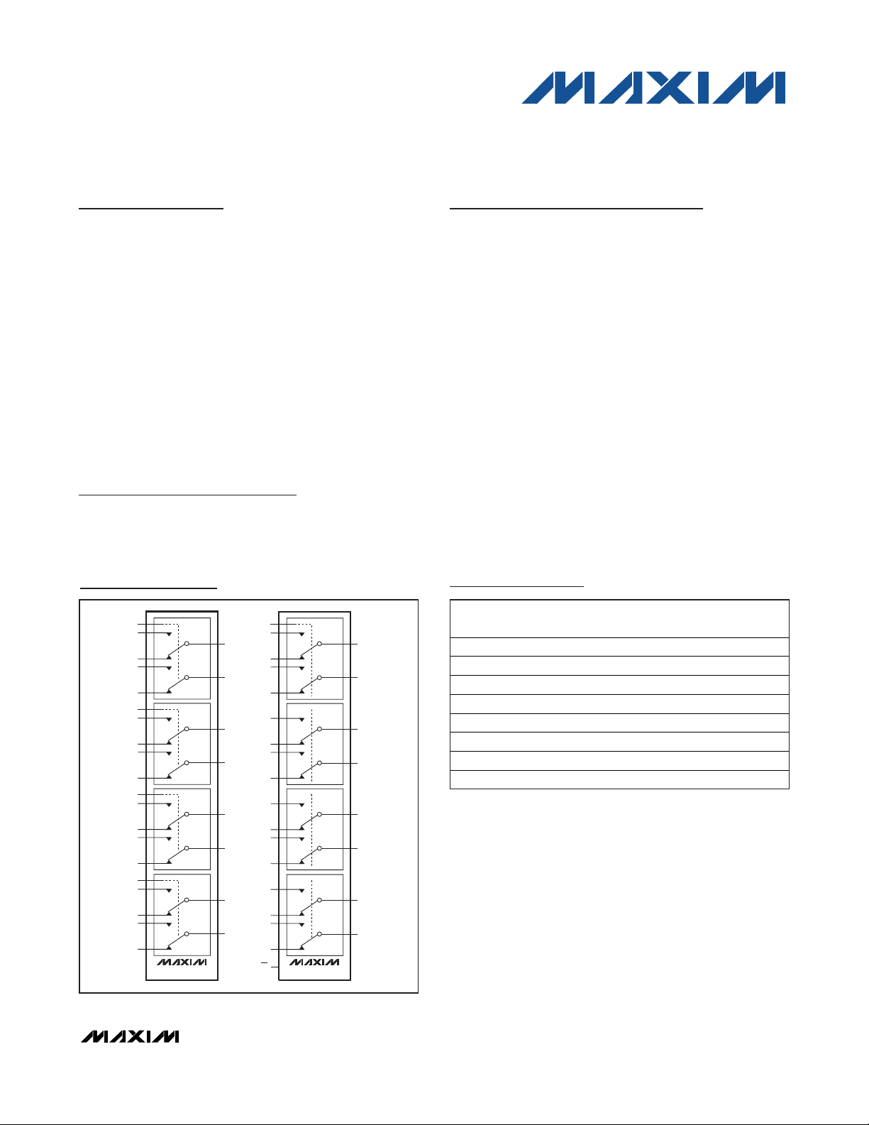
The MAX4760/MAX4760A are quad double-pole/double-throw (DPDT) switches, and the MAX4761/
MAX4761A are octal single-pole/double-throw (SPDT)
switches. They have eight 2.0Ω (typ) on-resistance,
low-capacitance switches to route audio and data signals. The MAX4760/MAX4760A have four logic inputs to
control the switches in pairs. The MAX4761/MAX4761A
have one logic control input and an enable input (EN)
to disable the switches.
The MAX4760/MAX4760A/MAX4761/MAX4761A are
available in a small 36-pin (6mm x 6mm) TQFN and
36-bump (3mm x 3mm) chip-scale package (UCSP™).
Applications
Features
♦ USB 1.1 and USB 2.0 (Full Speed 12Mbps)
Signal-Switching Compliant
♦ Data and Audio Signal Routing
♦ Low-Capacitance Data Switches
♦ Less than 0.2ns Skew
♦ -3dB Bandwidth: 150MHz (typ)
♦ 0.2Ω (typ) Channel-to-Channel Matching
♦ 0.8Ω (typ) On-Resistance Flatness
♦ Rail-to-Rail Signal Handling
♦ 0.03% (typ) THD
♦ +1.8V to +5.5V Supply Range
♦ Low Supply Current with 1.8V Logic Threshold
(MAX4760A/MAX4761A)
♦ Tiny 36-Bump UCSP (3mm x 3mm)
♦ 36-Pin TQFN (6mm x 6mm)
♦ -40°C to +85°C Operating Temperature Range
MAX4760/MAX4760A/MAX4761/MAX4761A
High-Bandwidth, Quad DPDT Switches
________________________________________________________________
Maxim Integrated Products
1
Ordering Information
19-3037; Rev 5; 4/09
For pricing, delivery, and ordering information, please contact Maxim Direct at 1-888-629-4642,
or visit Maxim’s website at www.maxim-ic.com.
UCSP is a trademark of Maxim Integrated Products, Inc.
Functional Diagrams
Pin Configurations/Truth Tables and Typical Operating Circuit
appear at end of data sheet.
*Future product—contact factory for availability.
**EP = Exposed Pad.
+
Denotes a lead(Pb)-free/RoHS-compliant package.
T = Tape and reel.
USB Signal Switching
Audio-Signal Switching
Cellular Phones
PDAs/Handheld Devices
Notebook Computers
NO1
NC1
NO2
NC2
NO3
NC3
NO4
NC4
NO5
NC5
NO6
NC6
NO7
NC7
NO8
NC8
INA
INB
INC
IND
DATA 1
DATA 2
DATA 3
DATA 4
DATA 5
DATA 6
DATA 7
DATA 8
MAX4760/MAX4760A
COM1
COM2
COM3
COM4
COM5
COM6
COM7
COM8
NO1
NC1
NO2
NC2
NO3
NC3
NO4
NC4
NO5
NC5
NO6
NC6
NO7
NC7
NO8
NC8
INA
EN
DATA 1
DATA 2
DATA 3
DATA 4
DATA 5
DATA 6
DATA 7
DATA 8
MAX4761/MAX4761A
COM1
COM2
COM3
COM4
COM5
COM6
COM7
COM8
PART
TEMP RANGE
MAX4760EBX+T -40°C to +85°C 36 UCSP
MAX4760ETX+T -40°C to +85°C 36 TQFN-EP**
MAX4760AEWX+T -40°C to +85°C 36 UCSP
MAX4760AETX+T* -40°C to +85°C 36 TQFN-EP**
MAX4761EBX+T -40°C to +85°C 36 UCSP
MAX4761ETX+T -40°C to +85°C 36 TQFN-EP**
MAX4761AEBX+T* -40°C to +85°C 36 UCSP
MAX4761AETX+T* -40°C to +85°C 36 TQFN-EP**
PINPACKAGE
MAX4760/MAX4760A/MAX4761/MAX4761A
High-Bandwidth, Quad DPDT Switches
2 _______________________________________________________________________________________
ABSOLUTE MAXIMUM RATINGS
ELECTRICAL CHARACTERISTICS
(V+ = +2.7V to +5.25V, TA= -40°C to +85°C, unless otherwise noted. Typical values are at V+ = 3V, TA= +25°C.) (Notes 2, 3)
Stresses beyond those listed under “Absolute Maximum Ratings” may cause permanent damage to the device. These are stress ratings only, and functional
operation of the device at these or any other conditions beyond those indicated in the operational sections of the specifications is not implied. Exposure to
absolute maximum rating conditions for extended periods may affect device reliability.
(All voltages referenced to GND.)
V+ .............................................................................-0.3V to +6V
IN_, EN (MAX4761) ..................................................-0.3V to +6V
IN_, EN (MAX4761A)....................................-0.3V to (V+ + 0.3V)
COM_, NO_, NC_ (Note 1) ...........................-0.3V to (V+ + 0.3V)
Continuous Current
NO_, NC_, COM_ .......................................................±100mA
Peak Current
(pulsed at 1ms, 10% duty cycle)................................±200mA
(pulsed at 1ms, 50% duty cycle)............................... ±300mA
Continuous Power Dissipation (T
A
= +70°C)
36-Bump UCSP (derate 15.3mW/°C above +70°C).... 1221mW
36-Pin TQFN (derate 26.3mW/°C above +70°C)......... 2105mW
Operating Temperature Range ...........................-40°C to +85°C
Junction Temperature......................................................+150°C
Storage Temperature Range .............................-65°C to +150°C
Lead Temperature (soldering, 10s) ................................ +300°C
Bump Temperature (soldering)
Infrared (15s) ...............................................................+220°C
Vapor Phase (60s) .......................................................+215°C
Note 1: Signals on NO_, NC_, COM_ exceeding V+ or GND are clamped by internal diodes. Limit forward-diode current to maximum
current rating.
,
_
)
)
)
_
_
_
PARAMETER SYMBOL CONDITIONS T
ANALOG SWITCH
V
,
Analog Signal Range
On-Resistance R
On-Resistance Match
Between Channels
On-Resistance Flatness R
NO_, NC_ Off-Leakage
Current
C OM_
V
N O_
ON
ΔR
ON
FLAT(ON
I
NO_(OFF),
I
NC_(OFF
V
N C
V+ = 2.7V, I
V
or V
NC_
NO
V+ = 2.7V, I
or V
V
NO_
NC_
V+ = 2.7V, I
or V
V
NC_
NO_
V+ = 3.6V;
= 3.3V, 0.3V;
V
COM
_
V
or V
NO
_
= 10mA,
COM
_
0V or V+ (Note 4)
_ =
= 10mA,
COM
_
= 1.5V (Notes 4, 5)
= 10mA,
COM
_
= 0V or V+ (Note 6)
= 0.3V, 3.3V
NC
_
V + = 3.6V ( M AX 4761/M AX 4761A) ;
= 3.3V , 0.3V ; V
COM_ Off-Leakage Current
COM_ On-Leakage Current I
COM_(ON
V
COM
_
V
= 0.3V , 3.3V
NC
_
V + = 3.6V ; V
or V
= 3.3V , 0.3V or unconnected
NC
= 3.3V , 0.3V ; V
COM
_
NO
or
_
NO
_
DYNAMIC
MAX4760/
MAX4761
MAX4760A/
Turn-On Time t
ON
V
NO
= 50Ω; CL = 35pF,
R
L
or V
NC
= 1.5V;
Figure 2
MAX4761A
A
T
to T
MIN
+25°C 2.0 3.5
to T
T
MIN
+25°C 0.2 0.4
T
to T
MIN
+25°C 0.8 1.5
T
to T
MIN
+25°C -5 +5
to T
T
MIN
+25°C -5 0.1 +5
T
to T
MIN
+25°C -5 +5
T
to T
MIN
+25°C 45 140
to T
T
MIN
+25°C 400 800
T
to T
MIN
MIN TYP MAX UNITS
MAX
MAX
MAX
MAX
MAX
MAX
MAX
MAX
MAX
0V+V
-25 +25
-25 +25
-25 +25
4
0.55
1.8
150
800
Ω
Ω
Ω
nA
nA
nA
ns
ns
MAX4760/MAX4760A/MAX4761/MAX4761A
High-Bandwidth, Quad DPDT Switches
_______________________________________________________________________________________ 3
ELECTRICAL CHARACTERISTICS (continued)
(V+ = +2.7V to +5.25V, TA= -40°C to +85°C, unless otherwise noted. Typical values are at V+ = 3V, TA= +25°C.) (Notes 2, 3)
),
)
)
)
PARAMETER SYMBOL CONDITIONS T
or
or V
MAX4760/
MAX4761
MAX4760A/
MAX4761A
= 1.5V;
NC
_
Turn-Off Time t
Break-Before-Make t
OFF
BBM
V+ = 2.7V, V
V
NC
_
= 50Ω; CL = 35pF,
R
L
= 1.5V;
NO
_
Figure 2
V+ = 2.7V, V
R
= 50Ω, CL = 35pF, Figure 3
L
NO
_
(Note 7)
Skew t
SKEW
Charge Injection Q
RS = 39Ω, CL = 50pF, Figure 4
(Note 7)
V
= 0V, R
GEN
C
= 1.0nF, Figure 5
L
GEN
= 0V,
A
+25°C 25 50
T
to T
MIN
+25°C 300 800
T
to T
MIN
+25°C 100
to T
T
MIN
+25°C 0.2 ns
+25°C 15 pC
On-Channel -3dB Bandwidth BW Signal = 0dBm, CL = 5pF, RL = 50Ω +25°C 150 MHz
Off-Isolation V
Crosstalk V
ISO
CT
Total Harmonic Distortion THD
C
NO_, NC_ Off-Capacitance
COM_ On-Capacitance C
COM_ Off-Capacitance C
NO_(OFF
C
NC_(OFF
COM(ON
COM(OFF
C L = 5p F, R
= 50Ω, V
L
f = 100kH z, Fi g ur e 6 (Note 8)
C L = 5p F, R
= 50Ω, V
L
f = 100kH z, Fi g ur e 6 (Note 9)
f = 20H z to 20kH z , V
DC bias = V+/2, R
V
, V
NO_
NC
L
= GND, f = 1MHz,
_
Figure 7
V
, V
NO_
= GND, f = 1MHz,
NC
_
Figure 7
V
= GND, f = 1MHz (MAX4761/
COM_
MAX4761A), Figure 7
COM_
COM_
COM_
= R
= 1V
= 1V
= 600Ω
S
= 1V
P-P
P-P,
P-P
,
+25°C 80 dB
,
+25°C 95 dB
+25°C 0.03 %
+25°C 25 pF
+25°C 54 pF
+25°C 25 pF
DIGITAL I/O (IN_, EN)
Input-Logic High V
Input-Logic Low V
Input Leakage Current IIN, I
V+ = 2.7V to 3.6V T
V+ = 3.6V to 5.5V
(MAX4760A/MAX4761A)
IH
V+ = 3.6V to 5.25V
(MAX4760/MAX4761)
V+ = 2.7V to 3.6V T
V+ = 3.6V to 5.5V
(MAX4760A/MAX4761A)
IL
V+ = 3.6V to 5.25V
(MAX4760/MAX4761)
VIN = 0V or V+ T
EN
T
T
T
T
MIN
MIN
MIN
MIN
MIN
MIN
MIN
to T
to T
to T
to T
to T
to T
to T
MIN TYP MAX UNITS
MAX
MAX
MAX
MAX
MAX
MAX
MAX
MAX
MAX
MAX
2
1.4
1.6
2.0
60
800
0.5
0.5
0.6
1µA
ns
ns
ns
V
V
MAX4760/MAX4760A/MAX4761/MAX4761A
High-Bandwidth, Quad DPDT Switches
4 _______________________________________________________________________________________
ELECTRICAL CHARACTERISTICS (continued)
(V+ = +2.7V to +5.25V, TA= -40°C to +85°C, unless otherwise noted. Typical values are at V+ = 3V, TA= +25°C.) (Notes 2, 3)
Note 2: The algebraic convention is used in this data sheet; the most negative value is shown in the minimum column.
Note 3: UCSP packages are 100% tested at +25°C and limits across the full temperature range are guaranteed by correlation and
design. TQFN packages are 100% tested at +85°C and limits across the full temperature range are guaranteed by correlation and design.
Note 4: R
ON
and ΔR
ON
matching specifications are guaranteed by design.
Note 5: ΔR
ON
= R
ON(MAX)
- R
ON(MIN)
.
Note 6: Flatness is defined as the difference between the maximum and minimum value of on-resistance as measured over the
specified analog signal ranges.
Note 7: Guaranteed by design, not production tested.
Note 8: Off-isolation = 20log
10[VCOM_
/(V
NO_
or V
NC_
)], V
COM_
= output, V
NO_
or V
NC_
= input to off switch.
Note 9: Between any two switches.
ON-RESISTANCE
vs. V
COM
AND TEMPERATURE
(MAX4760/MAX4761)
MAX4760A/61A toc03
V
COM
(V)
R
ON
(Ω)
4.54.03.53.02.52.01.51.00.5
1
2
3
4
5
0
0 5.0
V+ = 5V
TA = +85°C
TA = -40°C
TA = +25°C
ON-RESISTANCE
vs. V
COM
AND TEMPERATURE
(MAX4760/MAX4761)
MAX4760A/61A toc02
V
COM
(V)
R
ON
(Ω)
2.52.01.51.00.5
1
2
3
4
5
0
0 3.0
V+ = 3V
TA = +85°C
TA = -40°C
TA = +25°C
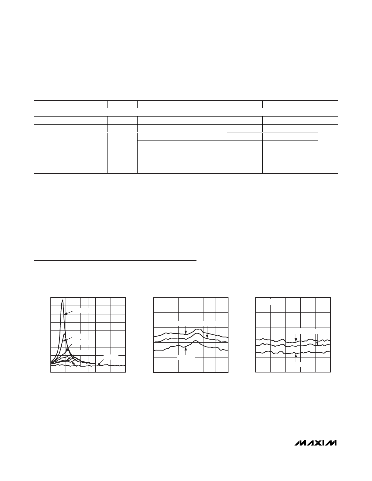
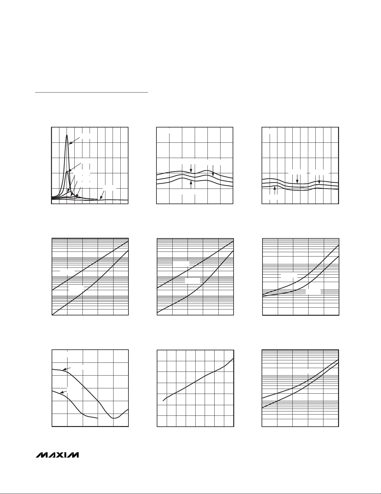
Typical Operating Characteristics
(V+ = 3V, TA= +25°C, unless otherwise noted.)
POWER SUPPLY
Power-Supply Range V+ T
Power Supply Current I+
PARAMETER SYMBOL CONDITIONS T
MIN
V+ = 4.3V, V
= 0V or V+
IN
_
(MAX4760/MAX4761)
V+ = 5.5V, V
= 0V or V+
IN
_
(MAX4760A/MAX4761A)
V+ = 5.5V, V
IN
= 1.8V
_
(MAX4760A/MAX4761A)
+25°C 0.01
T
MIN
+25°C 0.01
T
MIN
+25°C 5.5
T
MIN
A
to T
to T
to T
to T
MIN TYP MAX UNITS
1.8 5.5 V
MAX
MAX
MAX
MAX
1.0
1.0
12
µA
ON-RESISTANCE vs. V
(MAX4760/MAX4761)
10
9
8
7
6
(Ω)
ON
R
5
4
3
2
1
0 5.0
V+ = 1.8V
V+ = 2V
V+ = 2.3V
V+ = 3V
V+ = 2.7V
V
COM
(V)
COM
MAX4760A/61A toc01
V+ = 5V
4.54.03.0 3.51.0 1.5 2.0 2.50.5
MAX4760/MAX4760A/MAX4761/MAX4761A
High-Bandwidth, Quad DPDT Switches
_______________________________________________________________________________________
5
Typical Operating Characteristics (continued)
(V+ = 3V, TA= +25°C, unless otherwise noted.)
ON-RESISTANCE vs. V
COM
(MAX4760A/MAX4761A)
25
V+ = 1.8V
20
15
(Ω)
ON
R
10
5
0
0 5.0
V+ = 2V
V+ = 2.3V
V+ = 2.7V
V+ = 3V
V
COM
V+ = 5V
(V)
MAX4760A/61A toc04
4.54.03.53.02.52.01.51.00.5
NO/NC OFF-LEAKAGE CURRENT
vs. TEMPERATURE
10
1
V+ = 5V
0.1
V+ = 3V
0.01
NO/NC OFF-LEAKAGE CURRENT (nA)
MAX4760A/61A toc07
ON-RESISTANCE
AND TEMPERATURE
vs. V
COM
(MAX4760A/MAX4761A)
5
V+ = 3V
4
3
(Ω)
ON
R
2
1
0
0 3.0
TA = +85°C
TA = -40°C
V
COM
TA = +25°C
(V)
COM ON-LEAKAGE CURRENT
vs. TEMPERATURE
10
1
0.1
0.01
COM ON-LEAKAGE CURRENT (nA)
V+ = 5V
V+ = 3V
5
V+ = 5V
MAX4760A/61A toc05
2.52.01.51.00.5
MAX4760A/61A toc08
4
3
(Ω)
ON
R
2
1
0
0 5.0
10
1
0.1
COM OFF-LEAKAGE CURRENT (nA)
ON-RESISTANCE
AND TEMPERATURE
vs. V
COM
(MAX4760A/MAX4761A)
TA = +85°C
TA = -40°C
TA = +25°C
V
(V)
COM
COM OFF-LEAKAGE CURRENT
vs. TEMPERATURE
V+ = 5V
V+ = 3V
4.54.03.53.02.52.01.51.00.5
MAX4760A/61A toc06
MAX4760A/61A toc09
0.001
-40 85
TEMPERATURE (°C)
603510-15
0.001
-40 85
CHARGE INJECTION
vs. V
60
CL = 1nF
50
40
30
20
CHARGE INJECTION (pC)
10
0
05
V+ = 5V
V+ = 3V
COM
4321
V
(V)
COM
7.0
6.0
MAX4760A/61A toc10
5.0
4.0
3.0
SUPPLY CURRENT (nA)
2.0
1.0
0.0
vs. SUPPLY VOLTAGE
2.0 2.5 3.0 3.5 4.0 4.5 5.0 5.51.5
TEMPERATURE (°C)
SUPPLY CURRENT
SUPPLY VOLTAGE (V)
603510-15
0.01
-40 85
TEMPERATURE (°C)
603510-15
SUPPLY CURRENT
vs. TEMPERATURE
1000
MAX4760A/61A toc11
10
0.1
SUPPLY CURRENT (nA)
0.001
V+ = 5V
V+ = 3V
-40 85
TEMPERATURE (°C)
603510-15
MAX4760A/61A toc12

MAX4760/MAX4760A/MAX4761/MAX4761A
High-Bandwidth, Quad DPDT Switches
6 _______________________________________________________________________________________
Typical Operating Characteristics (continued)
(V+ = 3V, TA= +25°C, unless otherwise noted.)
LOGIC THRESHOLD
vs. SUPPLY VOLTAGE
MAX4760A/61A toc13
SUPPLY VOLTAGE (V)
LOGIC THRESHOLD (V)
5.04.54.03.53.02.52.0
0.4
0.8
1.2
1.6
2.0
0
1.5 5.5
V
IH
V
IL
TURN-ON/OFF TIME
vs. SUPPLY VOLTAGE
(MAX4760/MAX4761)
80
70
60
50
(ns)
OFF
40
/t
ON
t
30
20
10
0
1.5 5.5
t
ON
t
OFF
SUPPLY VOLTAGE (V)
1100
1000
900
MAX4760A/61A toc14
800
700
600
(ns)
OFF
500
/t
ON
t
400
300
200
100
5.04.52.0 2.5 3.0 3.5 4.0
0
1.5 5.5
TURN-ON/OFF TIME
vs. SUPPLY VOLTAGE
(MAX4760A/MAX4761A)
t
ON
t
OFF
MAX4760A/61A toc15
5.04.52.0 2.5 3.0 3.5 4.0
SUPPLY VOLTAGE (V)
TURN-ON/OFF TIMES
vs. TEMPERATURE
(MAX4760/MAX4761)
70
60
tON, V+ = 3V
50
40
(ns)
OFF
/t
t
tON, V+ = 5V
30
ON
20
t
, V+ = 3V
OFF
10
t
, V+ = 5V
OFF
0
-40 85
TEMPERATURE (°C)
FREQUENCY RESPONSE
20
0
-20
-40
-60
-80
ON-LOSS (dB)
-100
-120
-140
0.0001 0.01 1 100
ON-LOSS
OFF-ISOLATION
CROSS-TALK
FREQUENCY (MHz)
TURN-ON/OFF TIMES
vs. TEMPERATURE
(MAX4760A/MAX4761A)
600
500
MAX4760A/61A toc16
603510-15
tON, V+ = 3V
400
(ns)
tON, V+ = 5V
300
OFF
/t
ON
t
t
200
100
, V+ = 3V
OFF
t
, V+ = 5V
OFF
0
-40 85
10-15 35 60
TEMPERATURE (°C)
MAX4760A/61A toc17
TOTAL HARMONIC DISTORTION
vs. FREQUENCY
1
RL = 600Ω
MAX4760A/61A toc18
0.001
0.1
THD (%)
0.01
10 100 10,0001,000 100,000
FREQUENCY (Hz)
MAX4760A/61A toc19

MAX4760/MAX4760A/MAX4761/MAX4761A
High-Bandwidth, Quad DPDT Switches
_______________________________________________________________________________________ 7
Pin Description
PIN
MAX4760/MAX4760A MAX4761/MAX4761A
TQFN-EP UCSP TQFN-EP UCSP
1 A1 1 A1 NC1 Analog Switch 1, Normally Closed Terminal 1
2 B2 2 B2 COM2 Analog Switch 2, Common Terminal 2
3 A2 3 A2 NC2 Analog Switch 2, Normally Closed Terminal 2
4 A3 4 A3 INA
5 C3, D4 5 C3, D4 V+ Positive Supply Voltage
6 A4 — — INB Logic Control Digital Input for Switches 3 and 4
7 A5 7 A5 NC3 Analog Switch 3, Normally Closed Terminal 3
8 B5 8 B5 COM3 Analog Switch 3, Common Terminal 3
9 A6 9 A6 NC4 Analog Switch 4, Normally Closed Terminal 4
10 B6 10 B6 COM4 Analog Switch 4, Common Terminal 4
11, 14,
17, 29,
32, 35
12 C5 12 C5 NO3 Analog Switch 3, Normally Open Terminal 3
13 C6 13 C6 NO4 Analog Switch 4, Normally Open Terminal 4
15 D6 15 D6 NO8 Analog Switch 8, Normally Open Terminal 8
16 D5 16 D5 NO7 Analog Switch 7, Normally Open Terminal 7
18 E6 18 E6 COM8 Analog Switch 8, Common Terminal 8
19 F6 19 F6 NC8 Analog Switch 8, Normally Closed Terminal 8
20 E5 20 E5 COM7 Analog Switch 7, Common Terminal 7
21 F5 21 F5 NC7 Analog Switch 7, Normally Closed Terminal 7
22 F4 — — IND Logic Control Digital Input for Switches 7 and 8
23 C4, D3 23 C4, D3 GND Ground
24 F3 — — INC Logic Control Digital Input for Switches 5 and 6
25 F2 25 F2 NC6 Analog Switch 6, Normally Closed Terminal 6
26 E2 26 E2 COM6 Analog Switch 6, Common Terminal 6
27 F1 27 F1 NC5 Analog Switch 5, Normally Closed Terminal 5
28 E1 28 E1 COM5 Analog Switch 5, Common Terminal 5
30 D2 30 D2 NO6 Analog Switch 6, Normally Open Terminal 6
31 D1 31 D1 NO5 Analog Switch 5, Normally Open Terminal 5
33 C1 33 C1 NO1 Analog Switch 1, Normally Open Terminal 1
34 C2 34 C2 NO2 Analog Switch 2, Normally Open Terminal 2
36 B1 36 B1 COM1 Analog Switch 1, Common Terminal 1
— — 22 F4 EN Output Enable, Active Low
— — — — EP Exposed Pad (TQFN Only). Connect EP to GND.
—
6, 11, 14,
17, 24,
29, 32, 35
A4, F3 N.C. No Connection. Leave N.C. unconnected.
NAME FUNCTION
Logic Control Digital Input for the MAX4760/MAX4760A Switch 1
and Switch 2. Digital control input for all MAX4761/MAX4761A
switches.

MAX4760/MAX4760A/MAX4761/MAX4761A
High-Bandwidth, Quad DPDT Switches
8 _______________________________________________________________________________________
Detailed Description
The MAX4760/MAX4760A quad double-pole/doublethrow (DPDT) and the MAX4761/MAX4761A octal single-pole/double-throw (SPDT) analog switches operate
from a single +1.8V to +5.5V supply. These devices are
fully specified for +3V applications.
The MAX4760/MAX4760A/MAX4761/MAX4761A have a
guaranteed 2.0Ω (typ) on-resistance to switch data or
audio signals. The low 54pF (typ) capacitance and 0.2ns
change in skew makes them ideal for data switching
applications. The MAX4760/MAX4760A have four logic
inputs to control two switches in pairs and the
MAX4761/MAX4761A have one logic control input and an
enable input (EN) to disable the switches.
Applications Information
Digital Control Inputs
The MAX4760/MAX4760A/MAX4761/MAX4761A logic
inputs accept up to +5.5V regardless of the supply voltage. For example, with a +3.3V supply, IN_ can be driven low to GND and high to +5.5V, which allows mixed
logic levels in a system. Driving the control logic inputs
rail-to-rail also minimizes power consumption.
For the MAX4761/MAX4761A, drive EN low to enable.
When EN is high, COM_ is high impedance.
Analog Signal Levels
Analog signal inputs over the full voltage range (0V to V+)
are passed through the switch with minimal change in onresistance (see the
Typical Operating Characteristics
).
The switches are bidirectional so NO_, NC_, and COM_
can be either inputs or outputs.
Power-Supply Bypassing
Power-supply bypassing improves noise margin and
prevents switching noise from propagating from the V+
supply to other components. A 0.1µF capacitor connected from V+ to GND is adequate for most applications.
Power-Supply Sequencing
CMOS devices require proper power-supply sequencing. Always apply V+ before the analog signals, especially if the input signal is not current limited. If
sequencing is not possible, and the input signal is not
current limited to less than 20mA, add a small-signal
diode (Figure 1). Adding the diode reduces the analog
range to a diode drop (0.7V) below V+ and increases
the on-resistance slightly. The maximum supply voltage
must not exceed +6V at any time.
UCSP Applications Information
For the latest application details on UCSP construction,
dimensions, tape carrier information, printed circuit
board techniques, bump-pad layout, and recommended reflow temperature profile, as well as the latest information on reliability testing results, refer to the
Application Note 1891:
Wafer-Level Packaging (WLP)
and Its Applications
available on Maxim’s website at
www.maxim-ic.com/ucsp
.
Figure 1. Overvoltage Protection Using an External Blocking
Diode
POSITIVE SUPPLY
NO
V+
D1
COM
GND
MAX4760
MAX4761

MAX4760/MAX4760A/MAX4761/MAX4761A
High-Bandwidth, Quad DPDT Switches
_______________________________________________________________________________________ 9
Timing Circuits/Timing Diagrams
Figure 2. Switching Time
Figure 3. Break-Before-Make Interval
MAX4760/MAX4760A
MAX4761/MAX4761A
V
N_
LOGIC
INPUT
C
V
RL + R
MAX4760/MAX4760A
MAX4761/MAX4761A
V
N_
V+
V+
NO_
OR NC_
IN_
GND
INCLUDES FIXTURE AND STRAY CAPACITANCE.
L
R
= V
OUT
N_ (
NC_
NO_
IN_
COM_
R
L
L
)
ON
V+
V+
COM_
R
V+
LOGIC
INPUT
V
OUT
C
L
SWITCH
OUTPUT
V
OUT
L
C
L
0V
0V
LOGIC
INPUT
50%
V
OUT
0.9 x V
0UT
t
ON
IN DEPENDS ON SWITCH CONFIGURATION;
INPUT POLARITY DETERMINED BY SENSE OF SWITCH.
V+
50%
0V
tr < 5ns
tf < 5ns
50%
t
OFF
0.9 x V
OUT
LOGIC
INPUT
C
L
GND
INCLUDES FIXTURE AND STRAY CAPACITANCE.
0.9 x V
V
OUT
t
BBM
OUT

MAX4760/MAX4760A/MAX4761/MAX4761A
High-Bandwidth, Quad DPDT Switches
10 ______________________________________________________________________________________
Timing Circuits/Timing Diagrams (continued)
Figure 4. Input/Output Skew Timing Diagram
Figure 5. Charge Injection
t
ri
90%
t
fi
t
t
50%
50%
ro
50%
50%
fo
t
skew_i
10%
90%
t
skew_o
10%
TxD+
TxD-
R
s
MAX4760/MAX4760A
MAX4761/MAX4761A
R
Rs = 39Ω
C
L
s
= 50pF
A+
A-
B+
B-
C
L
C
L
INPUT A
INPUT A-
OUTPUT B
OUTPUT B-
10%
90%
10%
90%
|
DELAY DUE TO SWITCH FOR RISING INPUT AND RISING OUTPUT SIGNALS.
|t
ro - tri
|t
|
DELAY DUE TO SWITCH FOR FALLING INPUT AND FALLING OUTPUT SIGNALS.
fo - tfi
|
|t
CHANGE IN SKEW THROUGH THE SWITCH FOR OUTPUT SIGNALS.
skew_o
|t
|
CHANGE IN SKEW THROUGH THE SWITCH FOR INPUT SIGNALS.
skew_i
IN_
V+
V+
COM_
TO V
V
IL
IH
V
OUT
C
L
V
OUT
IN
OFF
OFF
IN
LOGIC INPUT WAVEFORMS INVERTED FOR SWITCHES
THAT HAVE THE OPPOSITE LOGIC SENSE.
Q = (ΔV
ON
ON
OUT
)(CL)
MAX4760/MAX4760A
MAX4761/MAX4761A
V
GEN
R
GEN
NC_
OR NO_
GND
ΔV
OUT
OFF
OFF

MAX4760/MAX4760A/MAX4761/MAX4761A
High-Bandwidth, Quad DPDT Switches
______________________________________________________________________________________ 11
Figure 6. On-Loss, Off-Isolation, and Crosstalk
Timing Circuits/Timing Diagrams (continued)
Figure 7. Channel On-/Off-Capacitance
Typical Operating Circuit
+5V
10nF
0V OR V+
50Ω
MEASUREMENTS ARE STANDARDIZED AGAINST SHORTS AT IC TERMINALS.
OFF-ISOLATION IS MEASURED BETWEEN COM_ AND OFF NO_ OR NC_ TERMINAL ON EACH SWITCH.
ON-LOSS IS MEASURED BETWEEN COM_ AND ON NO_ OR NC_ TERMINAL ON EACH SWITCH.
CROSSTALK IS MEASURED FROM ONE CHANNEL TO THE OTHER CHANNEL.
SIGNAL DIRECTION THROUGH SWITCH IS REVERSED; WORST VALUES ARE RECORDED.
IN_
NC1
V+
COM1
MAX4760/MAX4760A
MAX4761/MAX4761A
NO1*
GND
V+
10nF
V+
MAX4760/MAX4760A
MAX4761/MAX4761A
COM_
V
NETWORK
ANALYZER
V
IN
V
OUT
50Ω
MEAS REF
50Ω 50Ω
50Ω
OFF-ISOLATION = 20log
ON-LOSS = 20log
CROSSTALK = 20log
*FOR CROSSTALK THIS PIN IS NO2.
NC2 AND COM2 ARE OPEN.
OUT
V
IN
V
OUT
V
IN
V
OUT
V
IN
INA
NO1
NC1
NO2
NC2
COM1
COM2
HEADPHONES
RIGHT
HEADPHONES
LEFT
CAPACITANCE
METER
f = 1MHz
NC_ or
NO_
GND
IN
OR V
V
IL
IH
IND
NO7
NC7
NO8
NC8
COM7
SWITCHING DATA SIGNALS
COM8
MAX4760/
MAX4760A

MAX4760/MAX4760A/MAX4761/MAX4761A
High-Bandwidth, Quad DPDT Switches
12 ______________________________________________________________________________________
Pin Configurations/Truth Tables
TOP VIEW
(BUMP SIDE DOWN)
MAX4760/MAX4760A
1
234
+
NC1
A
COM1 COM2 COM3
B
NO1
C
NO5 NO6 GND V+
D
COM5 COM6
E
NC5 NC6 INC IND
F
NC2 INA
NO2 V+ GND
INB
UCSP
56
NC3
NO3 NO4
NO7 NO8
COM7 COM8
NC7 NC8
NC4
COM4
COM1
N.C.
+
36
35
NC1
1
2
COM2
3
NC2
INA
4
5
V+
6
INB
NC3
7
10
COM4
*EP
11
N.C.
8
COM3
9
NC4
*EXPOSED PADDLE CONNECTED TO GND.
NO5
N.C.
NO1
NO2
34
33
32
31
MAX4760/MAX4760A
12
13
14
15
NO4
NO3
N.C.
NO8
TQFN
NO6
30
16
NO7
MAX4760/MAX4760A
INA
NO1/NO2
LOW
HIGH
NO3/NO4 NC3/NC4
INB
LOW
HIGH
INC
NO5/NO6
LOW
HIGH
IND
LOW
HIGH
NO7/NO8
OFF
ON
OFF
ON
OFF
ON
OFF
ON
NC1/NC2
ON
OFF
ON
OFF
NC5/NC6
ON
OFF
NC7/NC8
ON
OFF
N.C.
29
17
N.C.
COM5
28
18
COM8
NC5
27
26
COM6
25
NC6
24
INC
23
GND
22
IND
NC7
21
20
COM7
19
NC8

MAX4760/MAX4760A/MAX4761/MAX4761A
High-Bandwidth, Quad DPDT Switches
______________________________________________________________________________________ 13
Pin Configurations/Truth Tables (continued)
Chip Information
PROCESS: CMOS
Package Information
For the latest package outline information and land patterns, go
to www.maxim-ic.com/packages
.
PACKAGE TYPE PACKAGE CODE DOCUMENT NO.
36 UCSP B36-2
21-0082
36 TQFN-EP T3666-3
21-0141
TOP VIEW
MAX4761/MAX4761A
(BUMP SIDE DOWN)
1
234
+
NC1
A
COM1 COM2 COM3
B
NO1
C
NO5 NO6 GND V+
D
COM5 COM6
E
NC5 NC6 N.C. EN
F
NC2 INA
NO2 V+ GND
UCSP
N.C.
56
NC3
NO3 NO4
NO7 NO8
COM7 COM8
NC7 NC8
NC4
COM4
MAX4761/MAX4761A
EN
LOW
LOW
HIGH
HIGH
INA
LOW
HIGH
X
X
COM1
+
36
NC1
1
2
COM2
3
NC2
INA
4
5
V+
6
N.C.
NC3
7
8
COM3
9
NC4
10
COM4
*EXPOSED PADDLE CONNECTED TO GND.
NO_
NC_
OFF
OFF
OFF
ON
ON
OFF
OFF
OFF
NO2
N.C.
35
34
MAX4761/MAX4761A
*EP
11
12
NO3
N.C.
NO1
33
13
NO4
TQFN
N.C.
32
14
N.C.
NO5
31
15
NO8
NO6
30
16
NO7
N.C.
29
17
N.C.
COM5
28
18
COM8
NC5
27
26
COM6
25
NC6
24
N.C.
23
GND
22
EN
NC7
21
20
COM7
19
NC8

MAX4760/MAX4760A/MAX4761/MAX4761A
High-Bandwidth, Quad DPDT Switches
Maxim cannot assume responsibility for use of any circuitry other than circuitry entirely embodied in a Maxim product. No circuit patent licenses are
implied. Maxim reserves the right to change the circuitry and specifications without notice at any time.
14
____________________Maxim Integrated Products, 120 San Gabriel Drive, Sunnyvale, CA 94086 408-737-7600
© 2009 Maxim Integrated Products Maxim is a registered trademark of Maxim Integrated Products, Inc.
Revision History
REVISION
NUMBER
4 4/07 Addition of MAX4760A/MAX4761A 1–14
5 4/09
REVISION
DATE
DESCRIPTION
Revised Ordering Information, Electrical Characteristics table, and Pin
Description.
PAGES
CHANGED
1, 3, 7
 Loading...