

19-0260; Rev 1; 3/95
Single/Dual/Quad, 10MHz
Single-Supply Op Amps
_______________General Description
The single MAX473, dual MAX474, and quad MAX475
are single-supply (2.7V to 5.25V), unity-gain-stable op
amps with rail-to-rail output swing. Each op amp guarantees a 10MHz unity-gain bandwidth, 15V/µs slew
rate, and 600Ω drive capability while typically consuming only 2mA supply current. In addition, the input
range includes the negative supply rail and the output
swings to within 50mV of each supply rail.
Single-supply operation makes these devices ideal for
low-power and low-voltage portable applications. With
their fast slew rate and settling time, they can replace
higher-current op amps in large-signal applications.
The MAX473/MAX474/MAX475 are available in DIP and
SO packages in the industry-standard op-amp pin
configurations. The MAX473 and MAX474 are also
offered in the µMAX package, the smallest 8-pin SO.
________________________Applications
Portable Equipment
Battery-Powered Instruments
Signal Processing
Discrete Filters
Signal Conditioning
Servo-Loops
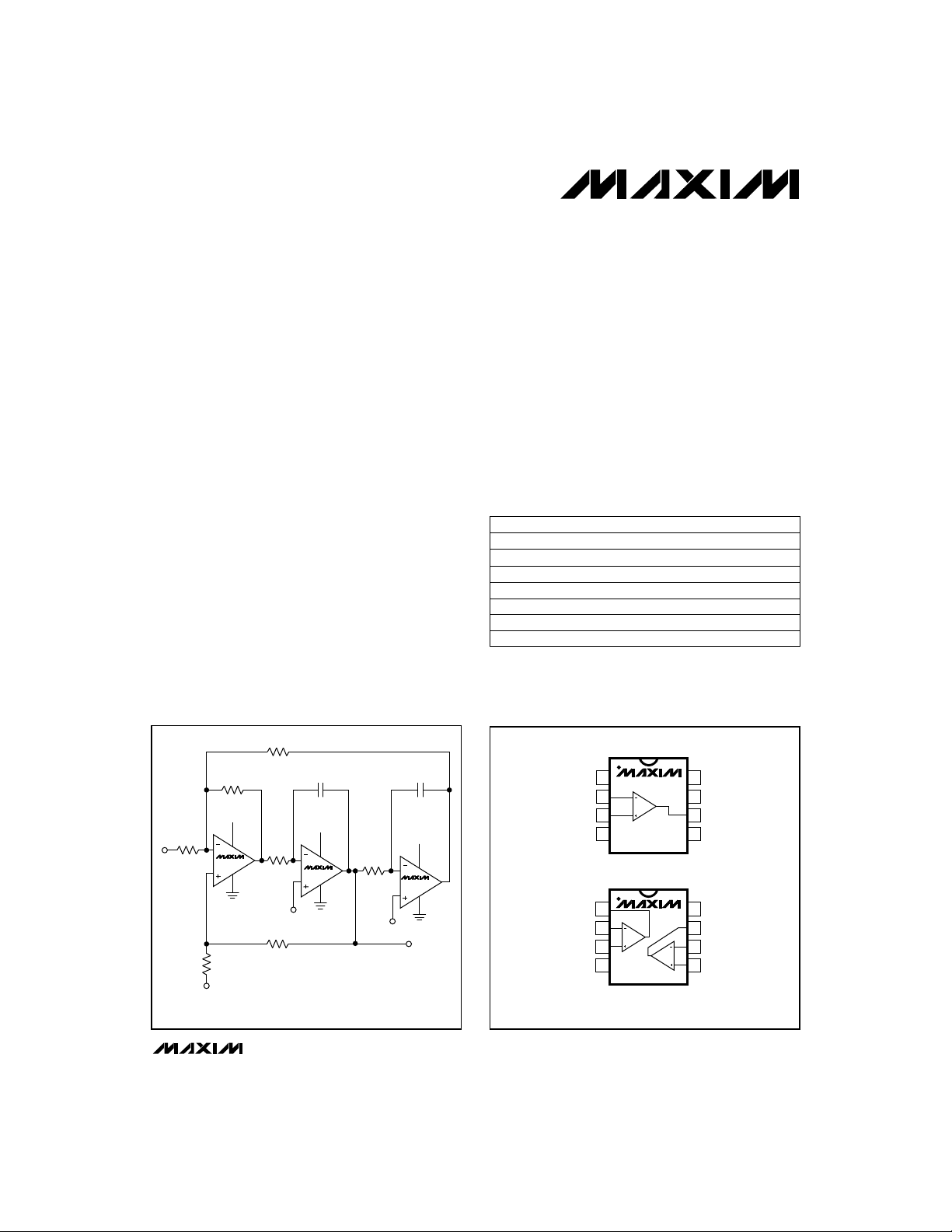
__________Typical Operating Circuit
____________________________Features
♦ 15V/µs Min Slew Rate
♦ +3V Single-Supply Operation
♦ Guaranteed 10MHz Unity-Gain Bandwidth
♦ 2mA Supply Current per Amplifier
♦ Input Range Includes Negative Rail
♦ Outputs Short-Circuit Protected
♦ Rail-to-Rail Output Swing (to within ±50mV)
♦ µMAX Package (the smallest 8-pin SO)
______________Ordering Information
PART
MAX473CPA
MAX473CSA
MAX473CUA 0°C to +70°C 8 µMAX
MAX473C/D 0°C to +70°C
MAX473EPA -40°C to +85°C 8 Plastic DIP
MAX473ESA -40°C to +85°C 8 SO
MAX473MJA -55°C to +125°C 8 CERDIP
Ordering Information continued on last page.
* Dice are specified at T
TEMP. RANGE PIN-PACKAGE
0°C to +70°C
0°C to +70°C
= +25°C, DC parameters only.
A
8 Plastic DIP
8 SO
Dice*
_________________Pin Configurations
MAX473/MAX474/MAX475
V
IN
100mVp-p
9.9k
9.9k
1V
9.9k
82pF
3V
1/4 MAX475
1V
BANDPASS OUTPUT
1Vp-p at 190kHz
9.9k
127k
1V
82pF
3V
1/4 MAX475
fo = 190kHz
Q = 10
9.9k
9.9k
3V
1/4 MAX475
BANDPASS FILTER
________________________________________________________________
TOP VIEW
1
NULL
IN+
V
OUTA
INAINA+
IN-
EE
EE
MAX473
2
3
4
DIP/SO/µMAX
1
2
A
3
4
DIP/SO/µMAX
Pin Configurations continued on last page.
Maxim Integrated Products
Call toll free 1-800-998-8800 for free samples or literature.
MAX474
B
8
NULL
7
V
CC
OUT
6
N.C.
5
8
V
CC
OUTB
7
INB-
6
INB+V
5
1
Single/Dual/Quad, 10MHz
Single-Supply Op Amps
ABSOLUTE MAXIMUM RATINGS
Supply Voltage (VCC- VEE)......................................................7V
Input Voltage (IN+, IN-, IN_+, IN_-).........................(V
Output Short-Circuit Duration.....................................Continuous
Continuous Power Dissipation (T
8-Pin Plastic DIP (derate 9.09mW/°C above +70°C) ...727mW
8-Pin SO (derate 5.88mW/°C above +70°C)................471mW
8-Pin µMAX (derate 4.1mW/°C above +70°C).............330mW
8-Pin CERDIP (derate 8.00mW/°C above +70°C)........640mW
14-Pin Plastic DIP (derate 10.00mW/°C above +70°C)...800mW
Stresses beyond those listed under “Absolute Maximum Ratings” may cause permanent damage to the device. These are stress ratings only, and functional
operation of the device at these or any other conditions beyond those indicated in the operational sections of the specifications is not implied. Exposure to
absolute maximum rating conditions for extended periods may affect device reliability.
= +70°C)
A
to (V
CC
EE
+ 0.3V)
- 0.3V)
ELECTRICAL CHARACTERISTICS
(+3V ≤ VCC≤ +5V, VEE= 0V, VCM= 0.5V, V
Input Offset Voltage ±0.70 ±2.0
Input Bias Current
MAX473/MAX474/MAX475
Input Offset Current
Common-Mode Voltage
Input Noise-Voltage Density
Large-Signal Gain
(Note 1)
Output Voltage
Unity-Gain Bandwidth
(Note 2)
V
V
A
V
GBW
= 0.5V, TA= +25°C, unless otherwise noted.)
OUT
CONDITIONS UNITSMIN TYP MAXSYMBOLPARAMETER
MAX473
MAX474
OS
MAX475
Current flows out of terminals
B
OS
High
CM
Low
VEE≤ VCM≤ (VCC- 1.9V)
VCC= 2.7V to 6.0V
f = 10kHz
n
0.3V ≤ V
(VCC- 0.5V)
VOL
Sinking 5mA
Sourcing 5mA
+ - VIN- = +1V, RL= no load
V
IN
OH
VIN+ - VIN- = -1V, RL= no load VEE+ 0.05
OL
VCC= 5V, RL= 10kΩ, CL= 20pF,
VIN+ - VIN- = +1V step
3V ≤ VCC≤ 5V 10 12
VCC= 2.7V 10
OUT
≤
14-Pin SO (derate 8.33mW/°C above +70°C)..............667mW
14-Pin CERDIP (derate 9.09mW/°C above +70°C)......727mW
Operating Temperature Ranges
MAX47_C_ _ ......................................................0°C to +70°C
MAX47_E_ _.....................................................-40°C to +85°C
MAX47_MJ_...................................................-55°C to +125°C
Junction Temperatures
MAX47_C_ _/E_ _........................................................ +150°C
MAX47_MJ_................................................................ +175°C
Storage Temperature Range.............................-65°C to +160°C
Lead Temperature (soldering, 10sec).............................+300°C
±0.70 ±2.0
±0.80 ±2.5
VCC- 1.9 VCC- 1.7
RL= no load
RL= 10kΩ
RL= 600Ω
VCC= 5V
VCC= 3V
VCC= 5V
VCC= 3V
VEE- 0.1 V
40e
110
94 105
82 90
76
100
76
90
VCC- 0.05V
15 17Slew Rate SR
EE
nV/√Hz
V/µs
MHz
mV
nA0 80 150I
nA±10 ±30I
V
dB80 90CMRRCommon-Mode Rejection Ratio
dB80 90PSRRPower-Supply Rejection Ratio
dB
V
2 _______________________________________________________________________________________
Single/Dual/Quad, 10MHz
Single-Supply Op Amps
ELECTRICAL CHARACTERISTICS (continued)
(+3V ≤ VCC≤ +5V, VEE= 0V, VCM= 0.5V, V
Settling Time
Power-Up Time
Overshoot
Phase Margin
Gain Margin
Supply Current
Operating Supply-Voltage
Range
= 0.5V, TA= +25°C, unless otherwise noted.)
OUT
CONDITIONS
To 0.1%, CL= 20pF
S
AV= +1, VIN= 1/2 VCCstep, see
PU
Operating Characteristics
CL= 150pF
CL= 20pF
VCC= 5V
VCC= 3V
VCC= 5V
VCC= 3V
S
RL= 10kΩ,
CL= 20pF
RL= 10kΩ,
CL= 20pF
Per amplifier
Single supply
Dual supplies
Typical
10
5
63
58
10
12
2.7 5.25
±1.35 ±2.625
ELECTRICAL CHARACTERISTICS
(+3V ≤ VCC≤ +5V, VEE= 0V, VCM= 0.5V, V
Input Offset Voltage ±2.0
Input Bias Current
Input Offset Current
Large-Signal Gain
(Note 1)
Output Voltage
Supply Current
Operating Supply-Voltage
Range
V
A
V
V
= 0.5V, TA= 0°C to +70°C, unless otherwise noted.)
OUT
CONDITIONS
MAX473
MAX474
OS
MAX475
Current flows out of terminals
B
OS
VEE≤ VCM≤ (VCC- 1.9V)
VCC= 2.7V to 6.0V
0.4V ≤ V
VOL
(VCC- 0.6V)
VIN+ - VIN- = +1V, RL= no load
OH
VIN+ - VIN- = -1V, RL= no load
OL
VCC= 5V, RL= 10kΩ, CL= 20pF,
VIN+ - VIN- = +1V step
Per amplifier
S
Single supply
Dual supplies
OUT
≤
RL= 10kΩ
RL= 600Ω
94
80
VCC- 0.07
VEE+ 0.07
12
2.7 5.25
±1.35 ±2.625
MAX473/MAX474/MAX475
UNITSMIN TYP MAXSYMBOLPARAMETER
ns400t
ns700t
%
degrees
dB
mA2.0 3.0I
V
UNITSMIN TYP MAXSYMBOLPARAMETER
±2.0
mV
±3.0
nA0 175I
nA±35I
dB78CMRRCommon-Mode Rejection Ratio
dB78PSRRPower-Supply Rejection Ratio
dB
V
V/µsSRSlew Rate
mA3.3I
V
_______________________________________________________________________________________ 3
Single/Dual/Quad, 10MHz
Single-Supply Op Amps
ELECTRICAL CHARACTERISTICS
(+3V ≤ VCC≤ +5V, VEE= 0V, VCM= 0.5V, V
Input Offset Voltage ±2.3
Input Bias Current
Input Offset Current
Large-Signal Gain
(Note 1)
Output Voltage
Supply Current
Operating Supply-Voltage
Range
V
A
V
V
= 0.5V, TA= -40°C to +85°C, unless otherwise noted.)
OUT
CONDITIONS
MAX473
MAX474
OS
MAX475
Current flows out of terminals
B
OS
VEE≤ VCM≤ (VCC- 2.0V)
VCC= 2.7V to 6.0V
0.4V ≤ V
VOL
(VCC- 0.6V)
VIN+ - VIN- = +1V, RL= no load
OH
VIN+ - VIN- = - 1V, RL= no load
OL
VCC= 5V, RL= 10kΩ, CL= 20pF,
VIN+ - VIN- = +1V step
Per amplifier
S
Single supply
Dual supplies
OUT
≤
RL= 10kΩ
RL= 600Ω
94
72
VCC- 0.08
10
2.7 5.25
±1.35 ±2.625
MAX473/MAX474/MAX475
ELECTRICAL CHARACTERISTICS
(+3V ≤ VCC≤ +5V, VEE= 0V, VCM= 0.5V, V
Input Offset Voltage ±2.8
Input Bias Current
Input Offset Current
Large-Signal Gain
(Note 1)
Output Voltage
Supply Current
Operating Supply-Voltage
Range
Note 1: Gain decreases to zero as the output swings beyond the specified limits.
Note 2: Guaranteed by correlation to slew rate.
V
A
V
= 0.5V, TA= -55°C to +125°C, unless otherwise noted.)
OUT
CONDITIONS
MAX473
MAX474
OS
MAX475
Current flows out of terminals
B
OS
VEE≤ VCM≤ (VCC- 2.15V)
VCC= 2.7V to 6.0V
0.5V ≤ V
VOL
(VCC- 0.6V)
VIN+ - VIN- = +1V, RL= no load
OH
VIN+ - VIN- = -1V, RL= no loadV
OL
VCC= 5V, RL= 10kΩ, CL= 20pF,
VIN+ - VIN- = +1V step
Per amplifier
S
Single supply
Dual supplies
OUT
≤
RL= 10kΩ
RL= 600Ω
90
70
VCC- 0.1
9
2.7 5.25
±1.35 ±2.625
±2.3
±3.3
VEE+ 0.08
±2.8
±4.0
VEE+ 0.1
UNITSMIN TYP MAXSYMBOLPARAMETER
mV
nA0 200I
nA±50I
dB72CMRRCommon-Mode Rejection Ratio
dB72PSRRPower-Supply Rejection Ratio
dB
V
V/µsSRSlew Rate
mA3.4I
V
UNITSMIN TYP MAXSYMBOLPARAMETER
mV
nA0 225I
nA±60I
dB70CMRRCommon-Mode Rejection Ratio
dB70PSRRPower-Supply Rejection Ratio
dB
V
V/µsSRSlew Rate
mA3.6I
V
4 _______________________________________________________________________________________

Single/Dual/Quad, 10MHz
Single-Supply Op Amps
__________________________________________Typical Operating Characteristics
(VCC= 5V, VEE= 0V, TA = +25°C, unless otherwise noted.)
SUPPLY CURRENT PER AMPLIFIER
3.0
2.5
2.0
(mA)
S
I
1.5
1.0
16
15
14
GBW (MHz)
13
12
vs. SUPPLY VOLTAGE
3 456
2
A
-60
VCC-VEE (V)
GAIN-BANDWIDTH PRODUCT
vs. TEMPERATURE
VCL = 40dB
-20 20 60 100 140
TEMPERATURE (°C)
MAX (V)
OUT
V
3.0
473 TOC-01
2.5
2.0
1.5
(mA)
S
I
1.0
0.5
0
20
473 TOC-04
17
14
SLEW RATE (V/µs)
11
8
MAXIMUM OUTPUT VOLTAGE
3.1
3.0
2.9
2.8
2.7
vs. LOAD RESISTANCE
VCC = 3V
V
1V
0.1 1 10 100 1000
LOAD RESISTANCE (kΩ)
SUPPLY CURRENT vs. TEMPERATURE
-60
-20 20 60 100 140
SLEW RATE vs. TEMPERATURE
-60
-20 20 60 100 140
CC
R
L
VCC = 5V
VCC = 3V
TEMPERATURE (°C)
VCC = 5V
VCC = 3V
TEMPERATURE (°C)
473 TOC-07
MIN (V)
OUT
V
INPUT BIAS CURRENT
120
473 TOC-02
100
80
60
(nA)
B
I
40
20
0
-60
-20 20 60 100 140
MAXIMUM OUTPUT VOLTAGE
5.2
473 TOC-05
5.1
5.0
MAX (V)
OUT
4.9
V
4.8
4.7
MINIMUM OUTPUT VOLTAGE
0.5
0.4
0.3
0.2
0.1
0
vs. LOAD RESISTANCE
VCC = 5V
VCC = 3V
0.1 1 10 100 1000 10,000
LOAD RESISTANCE (kΩ)
vs. LOAD RESISTANCE
VCC = 5V
0.1 1 10 100 1000
LOAD RESISTANCE (kΩ)
V
CC
1V
vs. TEMPERATURE
TEMPERATURE (°C)
1V
473 TOC-08
R
L
V
CC
R
L
MAX473/MAX474/MAX475
473 TOC-03
473 TOC-06
_______________________________________________________________________________________
5

Single/Dual/Quad, 10MHz
Single-Supply Op Amps
____________________________Typical Operating Characteristics (continued)
(VCC= 5V, VEE= 0V, TA = +25°C, unless otherwise noted.)
MINIMUM OUTPUT VOLTAGE
50
40
(mV)
I
OUT
30
-V
EE
V
I
20
MIN,
OUT
V
10
0
130
MAX473/MAX474/MAX475
110
90
70
50
OPEN-LOOP GAIN (dB)
30
10
vs. TEMPERATURE
V
1V
-60
-60
CC
VCC = 5V
VCC = 3V
-20 20 60 100 140
TEMPERATURE (°C)
OPEN-LOOP GAIN vs. TEMPERATURE
-20 20 60 100 140
RL = 10kΩ
RL = 600Ω
TEMPERATURE (°C)
100
INPUT REFERRED
CURRENT-NOISE DENSITY
vs. FREQUENCY
473 TOC-09
473 TOC-12
MAXIMUM OUTPUT VOLTAGE
20
15
(mV)
OUT
-V
CC
10
MAX, V
OUT
V
5
0
vs. TEMPERATURE
VCC = 5V
VCC = 3V
-60
-20 20 60 100 140
TEMPERATURE (°C)
OVERSHOOT vs. CAPACITIVE LOAD
40
RL = NO LOAD
30
20
OVERSHOOT (%)
10
0
1 10 1000
VCC = 3V
0.5V STEP
CAPACITIVE LOAD (pF)
473 TOC-15
OPEN-LOOP VOLTAGE GAIN
125
473 TOC-10
115
105
1V
V
CC
95
OPEN-LOOP VOLTAGE GAIN (dB)
85
1000
473 TOC-13
100
VCC = 5V
1.0V STEP
100
-60
-65
AV = +1
V
VOLTAGE-NOISE DENSITY (nV/√Hz)
10
TOTAL HARMONIC DISTORTION
AND NOISE vs. FREQUENCY
= 1.5Vp-p
IN
vs. LOAD RESISTANCE
VCC = 3V
VCC = 5V
0.1 1 10 100 1000 10,000
LOAD RESISTANCE (kΩ)
VOLTAGE-NOISE DENSITY
vs. FREQUENCY
INPUT REFERRED
10 100 1k 10k 100k
FREQUENCY (Hz)
473 TOC-17
473 TOC-11
473 TOC-14
-70
-75
THD + NOISE (dB)
-80
CURRENT-NOISE DENSITY (pA/√Hz)
10
10 100 1k 10k 100k
FREQUENCY (Hz)
-85
-90
10 100 1k 10k 100k
FREQUENCY (Hz)
6 _______________________________________________________________________________________

Single/Dual/Quad, 10MHz
Single-Supply Op Amps
____________________________Typical Operating Characteristics (continued)
(VCC= 5V, VEE= 0V, TA = +25°C, unless otherwise noted.)
POWER-SUPPLY REJECTION RATIO
80
70
60
50
PSRR (dB)
40
30
20
1 10 100 1000
vs. FREQUENCY
V
= 3V ± 300mV
CC
V
= 5V ± 250mV
CC
FREQUENCY (kHz)
GAIN AND PHASE vs. FREQUENCY
VCC = 3V
40
GAIN
20
PHASE
0
GAIN (dB)
-20
-40
1k 10k 100k 1M 10M
10k
100
473 TOC-23
GAIN (dB)
10k
20pF
FREQUENCY (Hz)
UNITY-GAIN FOLLOWER
FREQUENCY RESPONSE
VCC = 3V
1
= 10kΩ
L
GAIN
20pF
II
FREQUENCY (Hz)
180
144
473 TOC-21
108
PHASE (DEGREES)
72
36
0
-36
-72
-108
-144
-180
R
0
-1
PHASE
-2
-3
1k 10k 100k 1M 10M
180
144
473 TOC-19
108
PHASE (DEGREES)
72
36
0
-36
-72
-108
-144
-180
GAIN AND PHASE vs. FREQUENCY
VCC = 5V
40
GAIN
20
PHASE
0
GAIN (dB)
-20
-40
100
1k 10k 100k 1M 10M
GAIN (dB)
10k
10k
20pF
FREQUENCY (Hz)
-1
-2
-3
-4
UNITY-GAIN FOLLOWER
FREQUENCY RESPONSE
1
VCC = 5V
= 10kΩ
L
20pF
II
FREQUENCY (Hz)
180
144
473 TOC-22
108
PHASE (DEGREES)
72
36
0
-36
-72
-108
-144
-180
R
0
GAIN
PHASE
1k 10k 100k 1M 10M
MAX473/MAX474/MAX475
180
144
473 TOC-20
108
PHASE (DEGREES)
72
36
0
-36
-72
-108
-144
-180
0.1Hz to 10Hz VOLTAGE NOISE
1k
1k
POWER-UP TIME
100k
10pF
INPUT REFERRED VOLTAGE (2µV/div)
500ns/div
1sec/div
A : VCC, 5V/div
B : V
, 1V/div
OUT
_______________________________________________________________________________________
A
B
7

Single/Dual/Quad, 10MHz
Single-Supply Op Amps
____________________________Typical Operating Characteristics (continued)
(VCC= 5V, VEE= 0V, TA = +25°C, unless otherwise noted.)
SMALL-SIGNAL TRANSIENT RESPONSE
(V
= 5V)
CC
A
0.5V
B
0.5V
200ns/div
VCC = 5V, AV = +1, RL = 10kΩ, CL = 220pF
A : V
, 50mV/div
IN
B : V
, 50mV/div
OUT
MAX473/MAX474/MAX475
LARGE-SIGNAL TRANSIENT RESPONSE
A
0.5V
B
0.5V
200ns/div
= 5V, AV = +1, RL = 10kΩ, CL = 220pF
V
CC
A : V
, 1V/div
IN
B : V
, 500mV/div
OUT
SMALL-SIGNAL TRANSIENT RESPONSE
(V
= 3V)
CC
200ns/div
VCC = 3V, AV = +1, RL = 10kΩ, CL = 100pF
A : V
, 50mV/div
IN
B : V
, 50mV/div
OUT
OVERDRIVING THE OUTPUT
200ns/div
VCC = 5V, VIN- = 2.0V, RL = 10kΩ, CL = 33pF
A : V
+, 1V/div
IN
B : V
, 1V/div
OUT
A
0.5V
B
0.5V
A
1.5V
B
0V
8 _______________________________________________________________________________________

Single/Dual/Quad, 10MHz
Single-Supply Op Amps
______________________________________________________________Pin Description
MAX473
PIN
MAX474
—1, 8
MAX475
—
1
—
2
—
3
11
—
5
—
6
7
4
NAME
NULL
OUTA
IN-
INA-
IN+
INA+
V
EE
N.C.
INB+
OUT
INB-
OUTB
V
CC
FUNCTION
Offset Null Input. Connect to one end of 2kΩ potentiometer for offset voltage
trimming. Connect wiper to VEE. See Figure 1.
Amplifier A Output1—
Inverting Input—2
Amplifier A Inverting Input2—
Noninverting Input—3
Amplifier A Noninverting Input3—
Negative Power-Supply Pin. Connect to ground or a negative voltage.44
No Connect—not internally connected—5
Amplifier B Noninverting Input5—
Amplifier Output —6
Amplifier B Inverting Input6—
Amplifier B Output7—
Positive Power-Supply Pin. Connect to (+) terminal of power supply.87
Amplifier C OutputOUTC8——
Amplifier C Inverting InputINC-9——
Amplifier C Noninverting InputINC+10——
Amplifier D Noninverting InputIND+12——
Amplifier D Inverting InputIND-13——
Amplifier D OutputOUTD14——
MAX473/MAX474/MAX475
__________Applications Information
Power Supplies
The MAX473/MAX474/MAX475 operate from a single
2.7V to 5.25V power supply, or from dual supplies of
±1.35V to ±2.625V. For single-supply operation,
bypass the power supply with 0.1µF. If operating from
dual supplies, bypass each supply to ground. With
0.1µF bypass capacitance, channel separation
(MAX474/MAX475) is typically better than 120dB with
signal frequencies up to 300kHz. Increasing the
bypass capacitance (e.g. 10µF || 0.1µF) maintains
channel separation at higher frequencies.
Minimizing Offsets
The MAX473’s maximum offset voltage is ±2mV
(TA= +25°C). If additional offset adjustment is required,
connect a 2kΩ trim potentiometer between pins 1, 8, and
4 (Figure 1). Input offset voltage for the dual MAX474
and quad MAX475 cannot be externally trimmed.
_______________________________________________________________________________________ 9
The MAX473/MAX474/MAX475 are bipolar op amps
with low input bias currents. The bias currents at both
inputs flow out of the device. Matching the resistance
at the op amp’s inputs significantly reduces the offset
error caused by the bias currents. Place a resistor (R3)
from the noninverting input to ground when using the
inverting configuration (Figure 2a); place R3 in series
with the noninverting input when using the noninverting
configuration (Figure 2b). Select R3 such that the parallel combination of R2 and R1 equals R3. Adding R3 will
slightly increase the op amp’s voltage noise.
Output Loading and Stability
The MAX473/MAX474/MAX475 op amps are unity-gain
stable. Any op amp’s stability depends on the configuration, closed-loop gain, and load capacitance. The
unity-gain, noninverting buffer is the most sensitive gain
configuration, and driving capacitive loads decreases
stability.

Single/Dual/Quad, 10MHz
Single-Supply Op Amps
R2
2k
1
NULL
MAX473
4
V
EE
Figure 1. Offset Null Circuit
The MAX473/MAX474/MAX475 have excellent phase
MAX473/MAX474/MAX475
margin (the difference between 180° and the unity-gain
NULL
8
phase angle). It is typically 63° with a load of 10kΩ in
parallel with 20pF. Generally, higher phase margins
indicate greater stability.
Capacitive loads form an RC network with the op amp’s
output resistance, causing additional phase shift that
reduces the phase margin. Figure 3 shows the
MAX473/MAX474/MAX475 output response when driving a 390pF load in parallel with 10kΩ.
When driving large capacitive loads, add an output isolation resistor, as shown in Figure 4. This resistor
improves the phase margin by isolating the load
capacitance from the amplifier output. Figure 5 shows
the MAX473/MAX474/MAX475 driving a capacitive load
of 1000pF using the circuit of Figure 4.
Feedback Resistors
The feedback resistors appear as a resistance network
to the op amp’s feedback input (Figure 2). This resistance, combined with the op amp’s input and stray
capacitance (total input capacitance), forms a pole that
adds unwanted phase shift when either the total input
capacitance or feedback resistance is too large. For
example, using the noninverting configuration with a
gain of 10, if the total capacitance at the negative input
is 10pF and the effective resistance (R1 ||R2) is 9kΩ,
this RC network introduces a pole at fo= 1.8MHz. At
IN
V
IN
R3 = R2R1
R1
V
OUT
R3
R3 = R2R1
R3
V
OUT
R2
R1
, the pole introduces addi-
o
V
Figure 2a. Reducing Offset Error Due to Bias Current:
Inverting Configuration
Figure 2b. Reducing Offset Error Due to Bias Current:
Noninverting Configuration
input frequencies above f
tional phase shift, which reduces the overall bandwidth
and adversely affects stability. Choose feedback resistors small enough so they do not adversely affect the
op amp’s operation at the frequencies of interest.
Overdriving the Outputs
The output voltage swing for specified operation is from
(VEE+ 0.3V) to (VCC- 0.5V) (
see Electrical Characteristics
Exercising the outputs beyond these limits drives the output transistors toward saturation, resulting in bandwidth
degradation, response-time increase, and gain decrease
(which affects linearity). Operation in this region causes a
slight distortion in the output waveform, but does not
adversely affect the op amp.
).
10 ______________________________________________________________________________________

Driving 390pF in parallel with 10kΩ,
= 5V, buffer configuration
V
CC
Single/Dual/Quad, 10MHz
Single-Supply Op Amps
MAX473/MAX474/MAX475
Figure 3. MAX474 Driving 390pF
MAX473/MAX474/
MAX475
RL
10Ω
V
IN
Figure 4. Capacitive-Load Driving Circuit
V
OUT
C
L
Full-Power Bandwidth
The MAX473/MAX474/MAX475’s fast 15V/µs slew rate
maximizes full-power bandwidth (FPBW). The FPBW is
given by:
FPBW (Hz) = —————————————
π [V
SR
peak-to-peak(max)]
OUT
where the slew rate (SR) is 15V/µs min. Figure 6 shows
the full-power bandwidth as a function of the peak-topeak AC output voltage.
Figure 5. The MAX473 easily drives 1000pF using the
Capacitive-Load Driving Circuit (Figure 4).
100
SMALL-SIGNAL
10
1
FULL-POWER BANDWIDTH (MHz)
0.1
Figure 6. Full-Power Bandwidth vs. Peak-to-Peak AC Voltage
FULL-POWER
BANDWIDTH
01 342
OUTPUT VOLTAGE SWING (Vp-p)
GAIN BANDWIDTH
MAX473-FIG6
Layout
A good layout improves performance by decreasing
the amount of stray capacitance at the amplifier’s
inputs and output. Since stray capacitance might be
unavoidable, minimize trace lengths and resistor leads,
and place external components as close to the pins as
possible.
______________________________________________________________________________________ 11

Single/Dual/Quad, 10MHz
Single-Supply Op Amps
_Ordering Information (continued)
PART
MAX474CPA
MAX474CSA
MAX474CUA 0°C to +70°C 8 µMAX
MAX474C/D 0°C to +70°C
MAX474EPA -40°C to +85°C 8 Plastic DIP
MAX474ESA -40°C to +85°C 8 SO
MAX474MJA -55°C to +125°C 8 CERDIP
MAX475CPD
MAX475CSD 0°C to +70°C 14 SO
MAX475EPD -40°C to +85°C 14 Plastic DIP
MAX475ESD -40°C to +85°C 14 SO
MAX475MJD -55°C to +125°C 14 CERDIP
* Dice are specified at TA= +25°C, DC parameters only.
TEMP. RANGE PIN-PACKAGE
0°C to +70°C
0°C to +70°C
8 Plastic DIP
8 SO
Dice*
0°C to +70°C 14 Plastic DIP
____Pin Configurations (continued)
MAX473/MAX474/MAX475
TOP VIEW
OUTA
INAINA+
V
INB+
INB-
OUTB
1
2
A
3
CC
4
MAX475
5
B
6
7
OUTD
14
IND-
13
D
IND+
12
V
11
EE
INC+
10
C
INC-
9
OUTC
8
_________________Chip Topographies
MAX473
NULL
IN-
IN+
V
EE
0.052"
(1.321mm)
TRANSISTOR COUNT: 185
SUBSTRATE CONNECTED TO V
MAX474
V
CC
OUTA
INA-
INA+
EE
NULL
V
CC
0.065"
(1.651mm)
OUT
OUTB
INB-
0.084"
(2.134mm)
INB+
DIP/SO
VEE
0.058"
(1.473mm)
TRANSISTOR COUNT: 355
SUBSTRATE CONNECTED TO V
Maxim cannot assume responsibility for use of any circuitry other than circuitry entirely embodied in a Maxim product. No circuit patent licenses are
implied. Maxim reserves the right to change the circuitry and specifications without notice at any time.
12
__________________Maxim Integrated Products, 120 San Gabriel Drive, Sunnyvale, CA 94086 (408) 737-7600
© 1995 Maxim Integrated Products Printed USA is a registered trademark of Maxim Integrated Products.
EE
 Loading...