

Page 1
General Description
The MAX4754/MAX4754A/MAX4755/MAX4756/MAX4756A
low on-resistance, analog switches operate from a single
+1.8V to +5.5V supply. The MAX4754/MAX4754A and
MAX4755 are dual, double-pole, double-throw (DPDT)
switches. The MAX4756/MAX4756A are quad, single-pole
double-throw (SPDT) switches. They are configured to
route either audio or data signals.
The MAX4754/MAX4754A have four 0.5Ω SPDT switches for
audio-signal routing and two logic control inputs. The
MAX4755 has four 0.5Ω SPDT switches (with two
switches that have an additional 11Ω series resistor at
the NC terminals). This allows users to drive an 8Ω
speaker as a 32Ω load (ear speaker). The MAX4756/
MAX4756A have four 0.5Ω SPDT switches controlled by
one logic control input and an enable input (EN) to disable the switches.
The MAX4754/MAX4754A/MAX4755/MAX4756/MAX4756A
are available in a space-saving 16-pin TQFN and a tiny
16-bump, 2mm x 2mm chip-scale package (UCSP™).
Applications
Speaker-Headset Switching
Audio-Signal Routing
Cellular Phones
PDAs/Handheld Devices
Notebook Computers
Features
♦ Data and Audio-Signal Routing
♦ Low R
ON
(0.5Ω typ) Audio Switches
♦ 0.1Ω (typ) Channel-to-Channel Matching
♦ 0.2Ω (typ) On-Resistance Flatness
♦ 0.035% (typ) THD
♦ Improved Power-Supply Current for Non-
Rail-to-Rail Control Logic Inputs
(MAX4754A/MAX4756A)
♦ +1.8V to +5.5V Supply Range
♦ Rail-to-Rail Signal Handling
♦ 16-Bump UCSP (2mm x 2mm)
MAX4754/MAX4754A/MAX4755/MAX4756/MAX4756A
0.5Ω, Quad SPDT Switches in UCSP/QFN
________________________________________________________________ Maxim Integrated Products 1
Ordering Information
19-2942; Rev 1; 11/06
For pricing, delivery, and ordering information, please contact Maxim/Dallas Direct! at
1-888-629-4642, or visit Maxim’s website at www.maxim-ic.com.
EVALUATION KIT
AVAILABLE
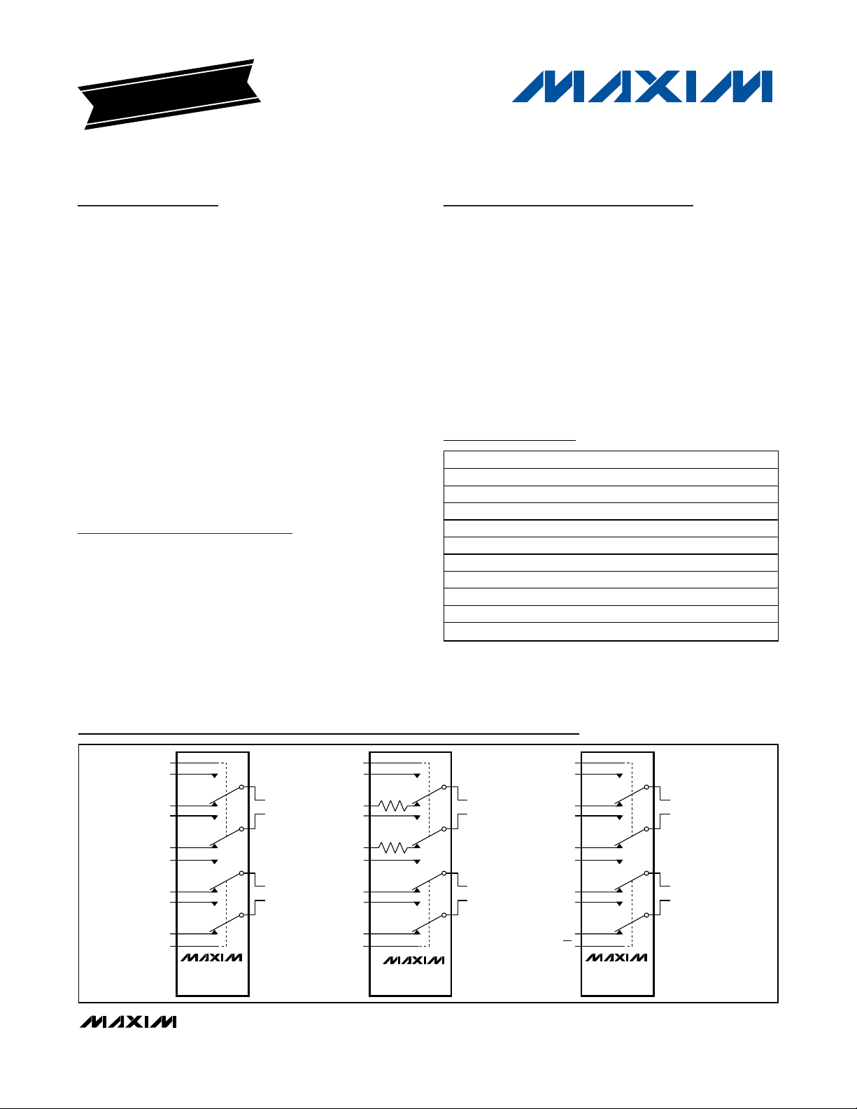
Functional Diagrams
UCSP is a trademark of Maxim Integrated Products, Inc.
Pin Configurations appear at end of data sheet.
Note: These devices operate over the -40°C to +85°C operating
temperature range.
*Future product—contact factory for availability.
**EP = Exposed paddle.
+Denotes lead-free package.
PART PIN-PACKAGE PKG CODE
MAX4754EBE+T 16 UCSP-16 B16-1
MAX4754ETE+T 16 TQFN-EP** T1644-4
MAX4754AEBE+T 16 UCSP-16 B16-1
MAX4754AETE+T 16 TQFN-EP** T1644-4
MAX4755EBE+T* 16 UCSP-16 B16-1
MAX4755ETE+T* 16 TQFN-EP** T1644-4
MAX4756EBE+T* 16 UCSP-16 B16-1
MAX4756ETE+T* 16 TQFN-EP** T1644-4
MAX4756AEBE+T* 16 UCSP-16 B16-1
MAX4756AETE+T* 16 TQFN-EP** T1644-4
INA
NO1
NC1
NO2
NC2
NO3
NC3
NO4
NC4
INB
MAX4754/
MAX4754A
COM1
COM2
COM3
COM4
INA
NO1
NC1
NO2
NC2
NO3
NC3
NO4
NC4
INB
11Ω
11Ω
MAX4755
COM1
COM2
COM3
COM4
INA
NO1
NC1
NO2
NC2
NO3
NC3
NO4
NC4
COM1
COM2
COM3
COM4
EN
MAX4756/
MAX4756A
Page 2
MAX4754/MAX4754A/MAX4755/MAX4756/MAX4756A
0.5Ω, Quad SPDT Switches in UCSP/QFN
2 _______________________________________________________________________________________
ABSOLUTE MAXIMUM RATINGS
ELECTRICAL CHARACTERISTICS
(V+ = +2.7V to +5.25V, TA= -40°C to +85°C, unless otherwise noted. Typical values are at +3V and TA= +25°C.) (Notes 2, 3)
Stresses beyond those listed under “Absolute Maximum Ratings” may cause permanent damage to the device. These are stress ratings only, and functional
operation of the device at these or any other conditions beyond those indicated in the operational sections of the specifications is not implied. Exposure to
absolute maximum rating conditions for extended periods may affect device reliability.
(All voltages referenced to GND.)
V+, IN_, EN...............................................................-0.3V to +6V
COM_, NO_, NC_ (Note 1) ...........................-0.3V to (V+ + 0.3V)
Continuous Current
NC1, NC2, COM1, COM2 (MAX4755)........................±100mA
NO_, NC_, COM_ (remaining terminal connections) ....±300mA
Peak Current NC1, NC2, COM1, COM2 (MAX4755)
(Pulsed at 1ms, 10% duty cycle)................................±200mA
(Pulsed at 1ms, 50% duty cycle)................................±150mA
Peak Current NO_, NC_,
COM__ (remaining terminal connections)
(Pulsed at 1ms, 10% duty cycle)............................±500mA
(Pulsed at 1ms, 50% duty cycle)............................±400mA
Continuous Power Dissipation (T
A
= +70°C)
16-Bump UCSP (derate 8.2mW/°C above +70°C) ......660mW
16-Pin TQFN (derate 16.9mW/°C
above +70°C)............................................................1349mW
ESD per Method 3015.7...................................................±2kV
Operating Temperature Range ...........................-40°C to +85°C
Junction Temperature......................................................+150°C
Storage Temperature Range .............................-65°C to +150°C
Bump Temperature (soldering)
Infrared (15s) ...............................................................+220°C
Vapor Phase (60s) .......................................................+215°C
Lead Temperature (soldering, 10s) .................................+300°C
Note 1: Signals on NO_, NC_, COM_ exceeding V+ or GND are clamped by internal diodes. Limit forward-diode current to maximum
current rating.
)
PARAMETER SYMBOL CONDITIONS T
ANALOG SWITCH
,
V
COM_
Analog Signal Range
On-Resistance R
V
V
NO_,
NC_
ON
V+ = 2.7V,
= 10mA,
I
COM_
V
_ or VNO_
NC
N_3, N_4), MAX4754/
MAX4754A/MAX4756/
MAX4756A
= 0V or V+
(Note 4)
MAX4755 (NC1, NC2)
MAX4755 (NO1, NO2,
V+ = 2.7V,
I
_ = 10mA,
COM
_ or VNO_
V
NC
N_3, N_4) MAX4754/
MAX4756
= +1.5V
On-Resistance Match
Between Channels
ΔR
ON
(Notes 4, 5)
MAX4755 (NC1, NC2)
V+ = +2.7V
_ = 10mA,
I
COM
V
_ or VNO_ =
NC
MAX4754A/MAX4756A
0 or V+
(Notes 4, 5)
V+ = 3V,
I
= 10mA,
On-Resistance Flatness R
FLAT(ON
COM_
_ or VNC_
V
NO
= 0V, 0.6V, or V+
(Note 6)
MAX4755
(NO1, NO2, N_3, N_4,
NO1, NO2), MAX4754/
MAX4754A/MAX4756/
MAX4756A
A
T
to
MIN
T
MAX
+25°C 0.5 0.85MAX4755 (NO1, NO2,
to
T
MIN
T
MAX
+25°C 11.5
T
to
MIN
T
MAX
+25°C 0.1 0.35
T
to
MIN
T
MAX
+25°C 0.2 0.4
T
to
MIN
T
MAX
+25°C 0.1 0.35
to
T
MIN
T
MAX
+25°C 0.2 0.4
T
to
MIN
T
MAX
MIN TYP MAX UNITS
0V+V
1.0
Ω
8.0 12.5
0.55
Ω
0.55
Ω
0.55
0.55
Ω
Page 3
MAX4754/MAX4754A/MAX4755/MAX4756/MAX4756A
0.5Ω, Quad SPDT Switches in UCSP/QFN
_______________________________________________________________________________________ 3
ELECTRICAL CHARACTERISTICS (continued)
(V+ = +2.7V to +5.25V, TA= -40°C to +85°C, unless otherwise noted. Typical values are at +3V and TA= +25°C.) (Notes 2, 3)
)
)
)
PARAMETER SYMBOL CONDITIONS T
NO_, NC_ Off-Leakage
Current
I
NO_(OFF),
I
NC_(OFF
V+ = 3.6V; V
V
or V
NO_
NC_
MAX4754/MAX4754A/MAX4755/MAX4756/
= 3.3V, 0.3V;
COM_
= 0.3V, 3.3V
MAX4756A
COM_ Off-Leakage
Current
COM_ On-Leakage
Current
I
COM_(OFF
I
COM_(ON
V+ = 3.6V (MAX4756/MAX4756A);
V
= 3.3V, 0.3V;
COM_
V
NO_
or V
= 0.3V, 3.3V
NC_
V+ = 3.6V;
V
= 3.3V, 0.3V;
COM_
V
NO_
or V
= 3.3V, 0.3V or unconnected
NC_
DYNAMIC
Turn-On Time NC_ t
Turn-Off Time NC_ t
Turn-On Time NO_ t
Turn-Off Time NO_ t
OFF, NO
Turn-On Time t
ON, NC
OFF, NC
ON, NO
ON
V+ = 2.7V, V
35pF (Figure 1) MAX4754A/MAX4756A
V+ = 2.7V, V
35pF (Figure 1) MAX4754A/MAX4756A
V+ = 2.7V, V
35pF (Figure 1) MAX4754A/MAX4756A
V+ = 2.7V, V
35pF (Figure 1) MAX4754A/MAX4756A
V+ = 2.7V, V
R
= 50Ω; CL = 35pF, (Figure 1)
L
= 1.5V, RL = 50Ω, CL =
NC_
= 1.5V, RL = 50Ω, CL =
NC_
= 1.5V, RL = 50Ω, CL =
NC_
= 1.5V, RL = 50Ω, CL =
NC_
NO_,
or V
NC_
= 1.5V;
MAX4754/MAX4755/MAX4756
Turn-Off Time t
OFF
V+ = 2.7V, V
= 50Ω; CL = 35pF (Figure 1)
R
L
NO_,
or V
NC_
= 1.5V;
MAX4754/MAX4755/MAX4756
Break-Before-Make t
BBM
Charge Injection Q V
On-Channel -3dB
Bandwidth
Off-Isolation V
Crosstalk V
BW
ISO
CT
V+ = 2.7V, V
= 50Ω, CL = 35pF (Figure 2) (Note 7)
R
L
= 0V , R
GE N
Signal = 0dBm, CL = 50pF, Rs = 50Ω,
= 50Ω
R
L
CL = 5pF, RL = 50Ω, V
f = 100kHz (Figure 4) (Note 8)
CL = 5pF, RL = 50Ω, V
f = 100kHz (Figure 4) (Note 9)
or V
NO_,
= 0, C L = 1.0nF ( Fi g ur e 3) +25°C 300 pC
GE N
NC_
COM
COM
= 1.5V;
_ = 1V
_ = 1V
P-P
P-P
+25°C -4 +4
T
MIN
T
MAX
+25°C -6 0.01 +6
T
MIN
T
MAX
+25°C -3 +3
T
MIN
T
MAX
+25°C 320 650
T
MIN
T
MAX
+25°C 27 60
T
MIN
T
MAX
+25°C 70 150
T
MIN
T
MAX
+25°C 300 650
T
MIN
T
MAX
+25°C 45 140
T
MIN
T
MAX
+25°C 25 50
T
MIN
T
MAX
+25°C 15
T
MIN
T
MAX
+25°C 10 MHz
+25°C -65 dB
+25°C -90 dB
MIN TYP MAX UNITS
A
to
-10 +10
to
-15 +15
to
-15 +15
to
to
to
to
to
to
to
2
900
70
200
900
150
60
nA
Ω
nA
ns
ns
ns
ns
ns
ns
ns
Page 4
MAX4754/MAX4754A/MAX4755/MAX4756/MAX4756A
0.5Ω, Quad SPDT Switches in UCSP/QFN
4 _______________________________________________________________________________________
Note 2: The algebraic convention is used in this data sheet; the most negative value is shown in the minimum column.
Note 3: UCSP parts are 100% tested at +25°C and limits across the full temperature range are guaranteed by correlation and
design. TQFN parts are 100% tested at +85°C and limits across the full temperature range are guaranteed by correlation
and design.
Note 4: R
ON
and ΔR
ON
matching specifications are guaranteed by design and correlation.
Note 5: ΔR
ON
= R
ON(MAX)
- R
ON(MIN)
.
Note 6: Flatness is defined as the difference between the maximum and minimum value of on-resistance as measured over the
specified analog signal ranges.
Note 7: Guaranteed by design, not production tested.
Note 8: Off-Isolation = 20log
10[VCOM
/ (V
NO
or VNC)], V
COM
= output, VNOor VNC= input to off switch.
Note 9: Between any two switches.
ELECTRICAL CHARACTERISTICS (continued)
(V+ = +2.7V to +5.25V, TA= -40°C to +85°C, unless otherwise noted. Typical values are at +3V and TA= +25°C.) (Notes 2, 3)
)
)
PARAMETER SYMBOL CONDITIONS T
Total Harmonic
Distortion
NO_, NC_ OffCapacitance
COM_ Off-Capacitance C
C
NO_(OFF)
C
NC_(OFF
COM_(OFF
COM_ On-Capacitance C
THD
(ON)
f = 20Hz to 20kHz, 1V
= 32Ω, VDC = V+/2
R
L
,
VNO, V
NC_
= GND,
f = 1MHz (Figure 5)
V
= G N D , f = 1M H z ( Fi g ur e 5) +25°C 300 pF
C OM _
V
= GND, f = 1MHz (Figure 5) +25°C 400 pF
COM_
P-P
,
DIGITAL I/O (IN_, EN)
V+ = 2.7V to 3.6V,
MAX4754/MAX4755/MAX4756
V+ = 2.7V to 5.25V,
IH
MAX4754A/MAX4756A
V+ = 3.6V to 5.25V,
MAX4754/MAX4755/MAX4756
V+ = 2.7V to 3.6V,
MAX4754/MAX4755/MAX4756
V+ = 2.7V to 5.25V,
IL
MAX4754A/MAX4756A
V+ = 3.6V to 5.25V,
MAX4754/MAX4755/MAX4756
Input Leakage Current I
IN
VIN = 0V or V+
POWER SUPPLY
Power-Supply Range V+
V+ = 5.5V, V
= 0V or V+,
IN_
MAX4754/MAX4754A/MAX4755/MAX4756/
MAX4756A
Power-Supply Current I+
V+ = 5.5V, V
= 0.5V or 1.4V,
IN_
MAX4754A/MAX4756A
+25°C 0.035 %
+25°C 180 pF
T
MIN
T
MAX
T
MIN
T
MAX
T
MIN
T
MAX
T
MIN
T
MAX
T
MIN
T
MAX
T
MIN
T
MAX
T
MIN
T
MAX
T
MIN
T
MAX
+25°C 0.2
T
MIN
T
MAX
+25°C 6.5
T
MIN
T
MAX
MIN TYP MAX UNITS
A
to
1.4
to
1.4Input Logic-High V
to
2.0
to
to
to
to
to
1.8 5.5 V
to
to
0.5
0.5Input Logic-Low V
0.6
1µA
2
12
V
V
µA
µA
Page 5
MAX4754/MAX4754A/MAX4755/MAX4756/MAX4756A
0.5Ω, Quad SPDT Switches in UCSP/QFN
_______________________________________________________________________________________ 5
Typical Operating Characteristics
(V+ = 3V, TA= +25°C, unless otherwise noted.)
ON-RESISTANCE vs. V
COM
(MAX4754A/MAX4756A)
4.5
4.0
3.5
3.0
2.5
(Ω)
ON
R
2.0
1.5
1.0
0.5
0
13.0
12.5
12.0
(Ω)
11.5
ON
R
11.0
V+ = 1.8V
V+ = 2.3V
V+ = 3.0V
(V)
V+ = 2.7V
V+ = 5.5V
COM
V+ = 2.7V
021345
V
COM
ON-RESISTANCE vs. V
MAX4755 NC1, NC2 CHANNELS
V+ = +1.8V
V+ = +2V
V+ = +2.3V
V+ = +2.5V
MAX4754A-56A toc01
MAX4754A-56A toc04
ON-RESISTANCE vs. V
AND TEMPERATURE
1.0
V+ = 3.0V
0.9
0.8
TA = +85°C
TA = -40°C
01
vs. V
COM
V+ = +3V
TA = +85°C
(_)
R
(Ω)
R
0.7
0.6
0.5
ON
0.4
0.3
0.2
0.1
0
13.0
12.5
12.0
11.5
ON
11.0
TA = +25°C
2
V
(V)
COM
ON-RESISTANCE
AND TEMPERATURE
MAX4755 NC1, NC2
CHANNELS
TA = +25°C
COM
1.0
0.9
0.8
MAX4754A-56A toc02
0.7
0.6
(_)
0.5
ON
R
0.4
0.3
0.2
0.1
3
13.0
12.5
MAX4754A-56A toc05
12.0
(Ω)
11.5
ON
R
11.0
ON-RESISTANCE vs. V
AND TEMPERATURE
V+ = +5.0V
TA = +85°C
TA = -40°C
0
021345
V
COM
ON-RESISTANCE
AND TEMPERATURE
vs. V
COM
V+ = +5V
TA = +85°C
TA = +25°C
COM
TA = +25°C
(V)
MAX4755 NC1, NC2
CHANNELS
MAX4754A-56A toc03
MAX4754A-56A toc06
V+ = +3.0V
10.5
10.0
0 5.0
V+ = +5V
V
COM
(V)
NO/NC OFF-LEAKAGE CURRENT
vs. TEMPERATURE
(MAX4754/MAX4755/MAX4756)
10
V+ = 5V
1
0.1
NO/NC OFF-LEAKAGE (nA)
0.01
-40 85
TEMPERATURE (°C)
10.5
4.54.03.0 3.51.0 1.5 2.0 2.50.5
10.0
0
TA = -40°C
V
COM
3.02.52.01.51.00.5
(V)
COM ON-LEAKAGE CURRENT
vs. TEMPERATURE
10
V+ = 5V
MAX4754A-56A toc07
603510-15
1
0.1
COM ON-LEAKAGE CURRENT (nA)
0.01
-40 85
TEMPERATURE (°C)
603510-15
10.5
10.0
120
110
100
90
MAX4754A-56A toc08
80
70
60
50
40
CHARGE INJECTION (pC)
30
20
10
0
TA = -40°C
0
V
COM
CHARGE INJECTION vs. V
(V)
5.04.53.52.5 4.03.02.01.51.00.5
COM
(MAX4754/MAX4755/MAX4756)
CL = 1nF
V+ = 5V
V+ = 3V
05
V
(V)
COM
4321
MAX4754A-56A toc09
Page 6

MAX4754/MAX4754A/MAX4755/MAX4756/MAX4756A
0.5Ω, Quad SPDT Switches in UCSP/QFN
6 _______________________________________________________________________________________
Typical Operating Characteristics (continued)
(V+ = 3V, TA= +25°C, unless otherwise noted.)
CHARGE INJECTION vs. V
COM
MAX4754A-56A toc10
V
COM
(V)
CHARGE INJECTION (pC)
4321
50
100
150
200
250
0
05
CI = 1nF
V+ = 5V
V+ = 3V
SUPPLY CURRENT
vs. SUPPLY VOLTAGE
MAX4754A-56A toc11
SUPPLY VOLTAGE (V)
SUPPLY CURRENT (nA)
5432
0.2
0.4
0.6
0.8
1.0
1.2
1.4
1.6
1.8
2.0
0
16
SUPPLY CURRENT vs. TEMPERATURE
(MAX4754/MAX4755/MAX4756)
MAX4754-56 toc12
TEMPERATURE (°C)
SUPPLY CURRENT (nA)
603510-15
0.01
0.1
1
10
100
0.001
-40 85
V+ = 5V
V+ = 3.0V
SUPPLY CURRENT vs. TEMPERATURE
(MAX4754A/MAX4756A)
MAX4754A-56A toc13
TEMPERATURE (°C)
SUPPLY CURRENT (nA)
6035-10-15
0.01
0.1
1
10
100
0.001
-40 85
V+ = 5.0V
V+ = 3.0V
LOGIC THRESHOLD vs. SUPPLY VOLTAGE
(MAX4754/MAX4755/MAX4756)
MAX4754A-56A toc14
SUPPLY VOLTAGE (V)
LOGIC THRESHOLD (V)
5.04.54.03.53.02.52.0
0.4
0.8
1.2
1.6
2.0
2.4
0
1.5 5.5
V
IH
V
IL
LOGIC THRESHOLD vs. SUPPLY VOLTAGE
(MAX4754A/MAX4756A)
MAX4754A-56A toc15
SUPPLY VOLTAGE (V)
LOGIC THRESHOLD (V)
4.53.52.5
0.2
0.4
0.6
0.8
1.0
1.2
1.4
0.0
1.5 5.5
V
IH
V
II
TURN-ON/OFF TIMES vs. SUPPLY VOLTAGE
(MAX4754/MAX4755/MAX4756)
MAx4754A-56A toc16
SUPPLY VOLTAGE (V)
t
ON
/t
OFF
(ns)
5.04.54.03.53.02.52.0
10
20
30
40
50
60
70
0
1.5 5.5
t
ON
t
OFF
TURN-ON/OFF TIMES vs. SUPPLY VOLTAGE
(MAX4754A)
SUPPLY VOLTAGE (V)
t
ON
/t
OFF
(ns)
MAX4754A-56A toc17
1.5 2.5 3.5 4.5 5.5
0
100
200
300
400
500
600
700
800
tON, NC
t
OFF
, NC
tON, NO
t
OFF
, NO
TURN-ON/OFF TIMES vs. TEMPERATURE
(MAX4754/MAX4755/MAX4756)
MAX4754A-56A toc18
TEMPERATURE (°C)
t
ON
/t
OFF
(ns)
603510-15
10
20
30
40
50
0
-40 85
tON, V+ = 3V
tON, V+ = 5V
t
OFF
, V+ = 5V
t
OFF
, V+ = 3V
Page 7

MAX4754/MAX4754A/MAX4755/MAX4756/MAX4756A
0.5Ω, Quad SPDT Switches in UCSP/QFN
_______________________________________________________________________________________ 7
Typical Operating Characteristics (continued)
(V+ = 3V, TA= +25°C, unless otherwise noted.)
TURN-ON/OFF TIMES vs. TEMPERATURE
(MAX4754A)
SUPPLY VOLTAGE (V)
t
ON
/t
OFF
(ns)
MAX4754A-56A toc19
-40 -15 10 35 60 85
0
50
100
150
200
250
300
350
400
450
tON, NC
t
OFF
, NO
tON, NO
t
OFF
, NC
SUPPLY CURRENT
vs. LOGIC CONTROL INPUT
IN_ (V)
CROWBAR CURRENT (nA)
MAX4754A-56A toc20
0123456
0
500
1000
1500
2000
2500
3000
3500
4000
V+ 5.5V
FREQUENCY REPSONSE
MAX4754A-56A toc21
FREQUENCY (MHz)
ON-LOSS (dB)
1010.001 0.01 0.1
-120
-100
-80
-60
-40
-20
0
20
-140
0.0001 100
ON-LOSS
OFF-ISOLATION
CROSS-TALK
TOTAL HARMONIC DISTORTION
PLUS NOISE vs. FREQUENCY
MAX4754A-56A toc22
FREQUENCY (kHz)
THD + N (%)
1010.1
0.01
0.1
1.0
0.001
0.01 100
RL = 32
Ω
Page 8

MAX4754/MAX4754A/MAX4755/MAX4756/MAX4756A
0.5Ω, Quad SPDT Switches in UCSP/QFN
8 _______________________________________________________________________________________
Pin Description
PIN
MAX4754/MAX4754A MAX4755 MAX4756/MAX4756A
UCSP QFN UCSP QFN UCSP QFN
C1 1 C1 1 C1 1 NO1 Analog Switch 1. Normally open terminal 1.
C2 2 C2 2 C2 2 INA
B1 3 B1 3 B1 3 COM1 Analog Switch 1. Common terminal.
A1 4 A1 4 A1 4 NC1 Analog Switch 1. Normally closed terminal 1.
A2 5 A2 5 A2 5 NO4 Analog Switch 4. Normally open terminal 4.
B2 6 B2 6 B2 6 V+ Positive Supply Voltage
A3 7 A3 7 A3 7 COM4 Analog Switch 4. Common terminal.
A4 8 A4 8 A4 8 NC4 Analog Switch 4. Normally closed terminal 4.
B4 9 B4 9 B4 9 NO2 Analog Switch 2. Normally open terminal 2.
B3 10 B3 10 — — INB Logic Control Digital Input for Switches 3 and 4
————B310EN Output Enable. Active low.
C4 11 C4 11 C4 11 COM2 Analog Switch 2. Common terminal 2.
D4 12 D4 12 D4 12 NC2 Analog Switch 2. Normally closed terminal 2.
D3 13 D3 13 D3 13 NO3 Analog Switch 3. Normally open terminal 3.
C3 14 C3 14 C3 14 GND Ground
D2 15 D2 15 D2 15 COM3 Analog Switch 3. Common terminal 3.
D1 16 D1 16 D1 16 NC3 Analog Switch 4. Normally closed terminal 3.
— EP — EP — EP EP Exposed Paddle. Connect EP to GND.
NAME FUNCTION
Logic Control Digital Input for Switches 1 and 2.
Digital control input for switches 1–4 for MAX4756.
Page 9

MAX4754/MAX4754A/MAX4755/MAX4756/MAX4756A
0.5Ω, Quad SPDT Switches in UCSP/QFN
_______________________________________________________________________________________ 9
Detailed Description
The MAX4754/MAX4754A/MAX4755/MAX4756/MAX4756A
low on-resistance analog switches operate from a single
+1.8V to +5.5V supply. The devices are fully specified
for nominal 3V applications.
The MAX4754/MAX4754A DPDT switch have two logic
control inputs with each input controlling two SPDT
switches. Each switch has a 0.5Ω on-resistance in the
NO and NC terminals making it ideal for switching
audio signals.
The MAX4755 DPDT switch also has four 0.5Ω SPDT
switches with the switch pairs 1 and 2 adding an 11.5Ω
series resistor to the NC terminal. This feature allows
the user to drive an 8Ω speaker as a 32Ω load, allowing
it to be used as an ear speaker. Two logic control
inputs are used to control the four switches.
The MAX4756/MAX4756A has four 0.5Ω SPDT switches
controlled by one logic control input (INA) and EN input
to disable the switches.
Applications Information
Digital Control Inputs
The MAX4754/MAX4754A/MAX4755/MAX4756/MAX4756A
logic inputs accept up to +5.5V regardless of the supply voltage. For example, with a +3.3V supply IN_ can
be driven low to GND and high to +5.5V, which allows
mixed logic levels in a system. Driving the control logic
inputs rail-to-rail also minimizes power consumption.
For a +3V supply voltage, the logic thresholds are 0.5V
(low) and 1.4V (high).
For the MAX4756/MAX4756A, drive EN low to enable the
COM_. When EN is high, COM _ is high impedance.
Analog Signal Levels
Analog signal inputs over the full voltage range (0V to
V+) are passed through the switch with minimal change
in on-resistance (see the Typical Operating Charac-
teristics). The switches are bidirectional so NO_, NC_,
and COM_ can be either inputs or outputs.
Power-Supply Bypassing
Power-supply bypassing improves noise margin and prevents switching noise from propagating from the V+ supply to other components. A 0.1µF capacitor connected
from V+ to GND is adequate for most applications.
UCSP Applications Information
For the latest application details on UCSP construction,
dimensions, tape carrier information, printed circuit
board techniques, bump-pad layout, and recommended reflow temperature profile, as well as the latest information on reliability testing results, go to the Maxim
website at www.maxim-ic.com/ucsp for the Application
Note: UCSP—A Wafer-Level Chip-Scale Package.
MAX4754/
MAX4754A
INA
NO1
NC1
NO2
NC2
NO3
NC3
NO4
NC4
INB
COM3
COM4
COM1
COM2
HEADPHONE
(32Ω)
INTERNAL
SPEAKER (8Ω)
MAX4755
INA
NO1
NC1
NO2
NC2
NO3
NC3
NO4
NC4
INB
COM3
COM4
COM1
COM2
CAR-KIT SPEAKER (8Ω)
EAR SPEAKER (32Ω)
LOUD SPEAKER (8Ω)
MAX4756/
MAX4756A
NO1
NC1
NO2
NC2
NO3
NC3
NO4
NC4
COM3
COM4
COM1
COM2
HEADPHONE
(32Ω)
11Ω
11Ω
EN
INA
INTERNAL
SPEAKER (8Ω)
Typical Operating Circuit
Page 10

MAX4754/MAX4754A/MAX4755/MAX4756/MAX4756A
0.5Ω, Quad SPDT Switches in UCSP/QFN
10 ______________________________________________________________________________________
Timing Circuits/Timing Diagrams
Figure 1. Switching Time
Figure 2. Break-Before-Make Interval
Figure 3. Charge Injection
MAX4754/MAX4754A
MAX4755/MAX4756/
MAX4756A
V
N_
LOGIC
INPUT
C
V
RL + R
MAX4754/MAX4754A
MAX4755/MAX4756/
MAX4756A
V
N_
V+
V+
NO_
OR NC_
IN_
GND
INCLUDES FIXTURE AND STRAY CAPACITANCE.
L
R
= V
OUT
N_ (
COM_
R
L
L
)
ON
V+
V+
NC_
NO_
IN_
COM_
R
L
V+
LOGIC
INPUT
V
OUT
C
L
SWITCH
OUTPUT
0V
0V
LOGIC
INPUT
V
OUT
C
L
50%
V
OUT
0.9 x V
0UT
t
ON
IN DEPENDS ON SWITCH CONFIGURATION;
INPUT POLARITY DETERMINED BY SENSE OF SWITCH.
V+
50%
0V
tr < 5ns
tf < 5ns
50%
t
OFF
0.9 x V
OUT
LOGIC
INPUT
C
L
GND
INCLUDES FIXTURE AND STRAY CAPACITANCE.
0.9 x V
V
OUT
t
BBM
OUT
MAX4754/MAX4754A
V+
MAX4755/MAX4756/
MAX4756A
V
GEN
R
GEN
NC_
OR NO_
GND
IN_
V+
COM_
TO V
V
IL
IH
V
OUT
C
L
V
OUT
IN
OFF
OFF
IN
Q = (ΔV
ON
ON
OUT
)(CL)
LOGIC INPUT WAVEFORMS INVERTED FOR SWITCHES
THAT HAVE THE OPPOSITE LOGIC SENSE.
ΔV
OUT
OFF
OFF
Page 11
MAX4754/MAX4754A/MAX4755/MAX4756/MAX4756A
0.5Ω, Quad SPDT Switches in UCSP/QFN
______________________________________________________________________________________ 11
Timing Circuits/Timing Diagrams (continued)
Figure 4. On-Loss, Off-Isolation, and Crosstalk
Figure 5. Channel On-/Off-Capacitance
10nF
+5V
0V OR V+
50Ω
MEASUREMENTS ARE STANDARDIZED AGAINST SHORTS AT IC TERMINALS.
OFF-ISOLATION IS MEASURED BETWEEN COM_ AND OFF NO_ OR NC_ TERMINAL ON EACH SWITCH.
ON-LOSS IS MEASURED BETWEEN COM_ AND ON NO_ OR NC_ TERMINAL ON EACH SWITCH.
CROSSTALK IS MEASURED FROM ONE CHANNEL TO THE OTHER CHANNEL.
SIGNAL DIRECTION THROUGH SWITCH IS REVERSED; WORST VALUES ARE RECORDED.
IN_
NC1
V+
MAX4754/MAX4754A
MAX4755/MAX4756/
MAX4756A
GND
COM1
NO1*
V+
10nF
V
NETWORK
ANALYZER
V
IN
V
OUT
50Ω
MEAS REF
50Ω 50Ω
50Ω
OFF-ISOLATION = 20log
ON-LOSS = 20log
CROSSTALK = 20log
*FOR CROSSTALK, THIS PIN IS NO2.
NC2 AND COM2 ARE OPEN.
OUT
V
IN
V
OUT
V
IN
V
OUT
V
IN
V+
MAX4754/MAX4754A/
MAX4755/MAX4756/
MAX4756A
COM_
CAPACITANCE
METER
f = 1MHz
NC_ or
NO_
GND
IN
OR V
V
IL
IH
Page 12

MAX4754/MAX4754A/MAX4755/MAX4756/MAX4756A
0.5Ω, Quad SPDT Switches in UCSP/QFN
12 ______________________________________________________________________________________
Pin Configurations/Truth Tables
Chip Information
PROCESS: CMOS
MAX4754
MAX4754A
MAX4755
TOP VIEW
(BUMP SIDE DOWN)
A
B
C
MAX4754/MAX4754A/MAX4755/
MAX4756/MAX4756A
1234
+
INB
(EN)
NC4
NO2
COM2
NC1
COM1
NO1
NO4
V+
INA
COM4
GND
NO3
GND
COM3
NC3
13
14
15
16
MAX4756
MAX4756A
NC2
EP*
COM2
101112
INB (EN)
9
NO2
8
NC4
7
COM4
V+
6
5
NO4
D
NC3
COM3
( ) FOR MAX4756/MAX4756A.
NO3
NC2
UCSP
MAX4754/MAX4754A/MAX4755
INA NO1/NO2 NC1/NC2 NO3/NO4 NC3/NC4
LOW OFF ON — —
HIGH ON OFF — —
INB
LOW — — OFF ON
HIGH — — ON OFF
+
NO1
INA
COM1
4321
NC1
TQFN
*EP: EXPOSED PADDLE CONNECTED TO GND.
MAX4756/MAX4756A
EN INA NO_ NC_
LOW LOW OFF ON
LOW HIGH ON OFF
HIGH X OFF OFF
HIGH X OFF OFF
Page 13

MAX4754/MAX4754A/MAX4755/MAX4756/MAX4756A
0.5Ω, Quad SPDT Switches in UCSP/QFN
______________________________________________________________________________________ 13
Package Information
(The package drawing(s) in this data sheet may not reflect the most current specifications. For the latest package outline information,
go to www.maxim-ic.com/packages
.)
24L QFN THIN.EPS
PACKAGE OUTLINE,
12, 16, 20, 24, 28L THIN QFN, 4x4x0.8mm
21-0139
1
E
2
Page 14
Package Information (continued)
(The package drawing(s) in this data sheet may not reflect the most current specifications. For the latest package outline information,
go to www.maxim-ic.com/packages
.)
MAX4754/MAX4754A/MAX4755/MAX4756/MAX4756A
0.5Ω, Quad SPDT Switches in UCSP/QFN
14 ______________________________________________________________________________________
PACKAGE OUTLINE,
12, 16, 20, 24, 28L THIN QFN, 4x4x0.8mm
21-0139
2
E
2
Page 15
MAX4754/MAX4754A/MAX4755/MAX4756/MAX4756A
0.5Ω, Quad SPDT Switches in UCSP/QFN
Maxim cannot assume responsibility for use of any circuitry other than circuitry entirely embodied in a Maxim product. No circuit patent licenses are
implied. Maxim reserves the right to change the circuitry and specifications without notice at any time.
Maxim Integrated Products, 120 San Gabriel Drive, Sunnyvale, CA 94086 408-737-7600 ____________________ 15
© 2006 Maxim Integrated Products is a registered trademark of Maxim Integrated Products, Inc.
Package Information (continued)
(The package drawing(s) in this data sheet may not reflect the most current specifications. For the latest package outline information,
go to www.maxim-ic.com/packages
.)
Revision History
Pages changed at Rev 1: 1–5, 7, 8, 13, 14, 15
16L,UCSP.EPS
PACKAGE OUTLINE, 4x4 UCSP
21-0101
1
H
1
 Loading...