

Page 1
General Description
The MAX4747–MAX4750 low-voltage, quad single-pole
single-throw (SPST)/dual single-pole/double-throw
(SPDT) analog switches operate from a single +2V to
+11V supply and handle rail-to-rail analog signals.
These switches exhibit low leakage current (0.1nA) and
consume less than 0.5nW (typ) of quiescent power,
making them ideal for battery-powered applications.
When powered from a +3V supply, these switches feature 50Ω (max) on-resistance (RON), with 3.5Ω (max)
matching between channels and 9Ω (max) flatness
over the specified signal range.
The MAX4747 has four normally open (NO) switches, the
MAX4748 has four normally closed (NC) switches, and
the MAX4749 has two NO and two NC switches. The
MAX4750 has two SPDT switches. These switches are
available in 14-pin TSSOP, 16-pin TQFN (4mm x 4mm),
and 16-bump WLP packages. This tiny chip-scale package occupies a 2mm 2mm area and significantly
reduces the required PC board area.
Applications
Battery-Powered Systems
Audio/Video-Signal Routing
Low-Voltage Data-Acquisition Systems
Cell Phones
Communications Circuits
Glucose Meters
PDAs
Features
o 2mm 2mm WLP
o Guaranteed On-Resistance (RON)
25Ω (max) at +5V
50Ω (max) at +3V
o On-Resistance Matching
3Ω (max) at +5V
3.5Ω (max) at +3V
o Guaranteed < 0.1nA Leakage Current at
TA= +25°C
o Single-Supply Operation from +2.0V to +11V
o TTL/CMOS-Logic Compatible
o -84dB Crosstalk (1MHz)
o -72dB Off-Isolation (1MHz)
o Low Power Consumption: 0.5nW (typ)
o Rail-to-Rail Signal Handling
MAX4747–MAX4750
50Ω, Low-Voltage, Quad SPST/Dual SPDT Analog
Switches in WLP
________________________________________________________________
Maxim Integrated Products
1
Ordering Information
19-2646; Rev 3; 1/12
For pricing, delivery, and ordering information, please contact Maxim/Dallas Direct! at
1-888-629-4642, or visit Maxim’s website at www.maxim-ic.com.
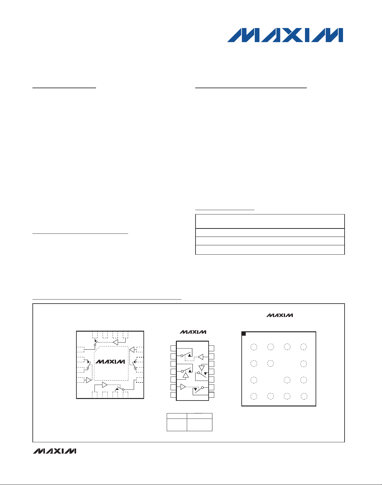
Pin/Bump Configurations/Truth Tables
Pin Configurations/Truth Tables continued at end of data sheet.
Ordering Information continued at end of data sheet.
*
EP = Exposed pad.
+
Denotes a lead(Pb)-free/RoHS-compliant package.
T = Tape and reel.
PART
TEMP
RANGE
MAX4747EUD+ -40°C to +85°C 14 TSSOP
MAX4747ETE+ -40°C to +85°C
MAX4747EWE+T -40°C to +85°C 16 WLP
PIN-/BUMPPACKAGE
16 Thin QFN-EP*
TOP VIEW
+
1
COM1
2
NO2
3
COM2
4
IN2
*CONNECT EP TO V+
NO1
V+
N.C.
IN1
16
15 14 13
MAX4747ETE
*EP
5678
IN3
GND
TQFN
NO3
N.C.
MAX4747
IN4
NO4
COM4
COM3
NO1
COM1
2
3
NO2
4
COM2
5
IN2
IN3
6
7
GND
INPUT SWITCH STATE
LOW
HIGH
TSSOP
12
11
10
9
+
1
14
13
12
11
10
9
8
OFF
ON
TOP VIEW
(BUMPS SIDE DOWN)
A
V+
IN1
B
IN4
NO4
COM4
C
COM3
NO3
D
MAX4747
1
234
NO2 COM2
COM1
NO1 V+ IN3
IN1 GND NO3
IN4 NO4 COM4 COM3
WLP
IN2
Page 2
MAX4747–MAX4750
50Ω, Low-Voltage, Quad SPST/Dual SPDT Analog
Switches in WLP
2 _______________________________________________________________________________________
ABSOLUTE MAXIMUM RATINGS
ELECTRICAL CHARACTERISTICS—Single +3V Supply
(V+ = +3V ±10%, VIH= +2.0V, VIL= +0.8V, TA= T
MIN
to T
MAX
, unless otherwise noted. Typical values are at V+ = +3V, TA= +25°C.)
(Notes 3, 4)
Stresses beyond those listed under “Absolute Maximum Ratings” may cause permanent damage to the device. These are stress ratings only, and functional
operation of the device at these or any other conditions beyond those indicated in the operational sections of the specifications is not implied. Exposure to
absolute maximum rating conditions for extended periods may affect device reliability.
(All voltages referenced to GND.)
V+ ...........................................................................-0.3V to +12V
IN_, COM_, NO_, NC_ (Note 1)....................-0.3V to (V+ + 0.3V)
Continuous Current (any pin) ...........................................±10mA
Peak Current (any pin, pulsed at 1ms, 10% duty cycle) ...±20mA
Continuous Power Dissipation (T
A
= +70°C)
14-Pin TSSOP (derate 9.1mW/°C above +70°C) .........727mW
16-Pin Thin QFN (derate 16.9mW/°C above +70°C) .....1349mW
16-Bump WLP (derate 7.3mW/°C above +70°C).........589mW
Operating Temperature Range ...........................-40°C to +85°C
Storage Temperature Range .............................-65°C to +150°C
Maximum Junction Temperature .....................................+150°C
Bump Temperature (soldering)
Infrared (15s) ...............................................................+220°C
Vapor Phase (60s) .......................................................+215°C
Lead Temperature (soldering, 10s) .................................+300°C
Soldering Temperature (reflow) .......................................+260°C
Note 1: Signals on IN_, NO_, NC_, or COM_ exceeding V+ or GND are clamped by internal diodes. Limit forward-diode current to
maximum current rating.
)
),
)
)
)
PARAMETER SYMBOL CONDITIONS T
ANALOG SWITCH
V
,
Analog Signal Range
On-Resistance R
V
NO_
COM_
, V
ON
NC_
On-Resistance Matching
Between Channels
∆R
ON
(Notes 5, 6)
On-Resistance Flatness
(Note 7)
NO_ or NC_ Off-Leakage Current
(Note 8)
COM_ Off-Leakage Current
(Note 8)
R
FLAT(ON
I
NO_(OFF
I
NC_(OFF
I
COM_(OFF
V+ = +2.7V, I
or V
V
NO_
NC_
V+ = +2.7V, I
or V
V
NO_
NC_
V+ = +2.7V, I
V
or V
NO_
NC_
V+ = +3.6V,
= +0.3V, +3V,
V
COM_
V
or V
NO_
NC_
V+ = +3.6V,
V
= +0.3V, +3V,
COM_
or V
V
NO_
NC_
MIN TYP MAX UNITS
A
0V+V
+25°C 17 50
= 5mA,
COM_
= +1.5V
T
T
MIN
MAX
to
60
+25°C 0.2 3.5
= 5mA,
COM_
= +1.5V
T
T
MIN
MAX
to
4.5
+25°C 2.7 9
= 5mA,
COM_
= +1V, +1.5V, +2V
T
T
MIN
MAX
to
11
+25°C -0.1 +0.1
= +3V, +0.3V
T
MIN
MAX
-2 +2
to
T
+25°C -0.1 +0.1
T
to
= +3V, +0.3V
T
MIN
MAX
-2 +2
Ω
Ω
Ω
nA
nA
COM_ On-Leakage Current
(Note 8)
I
COM_(ON
V+ = +3.6V,
= +0.3V, +3.0V,
V
COM_
V
or V
NO_
NC_
unconnected
= +0.3V, +3V, or
+25°C -0.2 +0.2
to
T
T
MIN
MAX
-4 +4
nA
Page 3
MAX4747–MAX4750
50Ω, Low-Voltage, Quad SPST/Dual SPDT Analog
Switches in WLP
_______________________________________________________________________________________ 3
ELECTRICAL CHARACTERISTICS—Single +3V Supply (continued)
(V+ = +3V ±10%, VIH= +2.0V, VIL= +0.8V, TA= T
MIN
to T
MAX
, unless otherwise noted. Typical values are at V+ = +3V, TA= +25°C.)
(Notes 3, 4)
)
)
PARAMETER SYMBOL CONDITIONS T
DYNAMIC
Turn-On Time t
Turn-Off Time t
ON
OFF
Break-Before-Make
(MAX4749/MAX4750 Only)
t
BBM
(Note 8)
Charge Injection Q
On-Channel -3dB Bandwidth BW Signal = 0dBm, 50Ω in and out +25°C 250 MHz
Off-Isolation (Note 9) V
Crosstalk (Note 10) V
NO_ or NC_ Off-Capacitance C
COM_ Off-Capacitance C
COM_ On-Capacitance C
ISO
CT
OFF
COM_(OFF
COM_(ON
LOGIC INPUT
Input Logic High V
Input Logic Low V
Input Leakage Current I
IH
IL
IN
POWER SUPPLY
Power-Supply Range V+ 2 11 V
Positive Supply Current I+
MIN TYP MAX UNITS
A
+25°C 57 150
V
or V
NO_
= 300Ω, CL = 35pF, Figure 2
R
L
NC_
= +1.5V,
T
T
MIN
MAX
to
170
+25°C 24 60
V
or V
NO_
R
= 300Ω, CL = 35pF, Figure 2
L
NC_
= +1.5V,
T
T
MIN
MAX
to
70
+25°C 33
V
or V
NO_
R
= 300Ω, CL = 35pF, Figure 3
L
= 0V , R
V
GE N
Figure 4
f = 1MHz, V
R
= 50Ω, CL = 5pF, Figure 5
L
f = 1MHz, V
R
= 50Ω, CL = 5pF, Figure 6
L
= +1.5V,
NC_
= 0Ω, C L = 1.0nF,
GE N
= 1V
NO_
= 1V
NO_
RMS
RMS
T
to
T
MIN
MAX
1
+25°C 7 pC
,
,
+25°C -72 dB
+25°C 84 dB
f = 1MHz, Figure 7 +25°C 20 pF
f = 1MHz, Figure 7 +25°C 20 pF
f = 1MHz, Figure 7 +25°C 40 pF
1.4 V
0.8 V
V
= 0V or V+ -1 +0.005 +1 µA
IN_
V+ = +5.5V, V
all switches on or off
= 0V or V+,
IN_
0.0001 1 µA
ns
ns
ns
Page 4
MAX4747–MAX4750
50Ω, Low-Voltage, Quad SPST/Dual SPDT Analog
Switches in WLP
4 _______________________________________________________________________________________
ELECTRICAL CHARACTERISTICS—Single +5V Supply
(V+ = +5V ±10%, VIH= +2.0V, VIL= +0.8V, TA= T
MIN
to T
MAX
, unless otherwise noted. Typical values are at V+ = +5V, TA= +25°C.)
(Notes 3, 4)
)
),
)
)
)
PARAMETER SYMBOL CONDITIONS T
ANALOG SWITCH
V
,
Analog Signal Range
On-Resistance R
V
NO_
COM_
, V
ON
NC_
On-Resistance Matching
Between Channels
∆R
ON
(Notes 5, 6)
On-Resistance Flatness
(Notes 7)
R
FLAT(ON
NO_ or NC_ Off-Leakage Current
(Note 8)
COM_ Off-Leakage Current
(Note 8)
I
NO_(OFF
I
NC_(OFF
I
COM_(OFF
V+ = +4.5V,
= 5mA,
I
COM_
V
or V
NO_
NC_
V+ = +4.5V, I
V
or V
NO_
NC_
V+ = +4.5V, I
V
or V
NO_
NC_
V+ = +5.5V,
= +1V, +4.5V,
V
COM_
V
or V
NO_
NC_
V+ = +5.5V,
V
= +1V, +4.5V,
COM_
or V
V
NO_
NC_
MIN TYP MAX UNITS
A
0V+V
+25°C 8.2 25
= +3.0V
T
MIN
MAX
30
to
T
+25°C 0.1 3
= 5mA,
COM_
= +3.0V
T
T
MIN
MAX
to
4
+25°C 2.2 5
= 5mA,
COM_
= +1V, +2V, +3V
T
T
MIN
MAX
to
7
+25°C -0.1 +0.1
= +4.5V, +1V
T
MIN
MAX
-2 +2
to
T
+25°C -0.1 +0.1
to
T
= +4.5V, +1V
T
MIN
MAX
-2 +2
Ω
Ω
Ω
nA
nA
COM_ On-Leakage Current
(Note 8)
I
COM_(ON
DYNAMIC
Turn-On Time t
Turn-Off Time t
ON
OFF
Break-Before-Make
(MAX4749/MAX4750 Only)
t
BBM
(Note 8)
Charge Injection Q
On-Channel -3dB Bandwidth BW
Off-Isolation (Note 9) V
ISO
V+ = +5.5V,
= +1V, +4.5V,
V
COM_
V
NO_
or V
= +1V, +4.5V, or
NC_
unconnected
V
or V
NO_
= 300Ω, CL = 35pF,
R
L
NC_
= +3.0V,
Figure 2
V
or V
NO_
R
= 300Ω, CL = 35pF,
L
NC_
= +3.0V,
Figure 2
V
or V
NO_
= 300Ω, CL = 35pF,
R
L
NC_
= +3.0V,
Figure 3
V
= 0V, R
GEN
= 1.0nF, Figure 4
C
L
GEN
= 0Ω,
Signal = 0dBm,
50Ω in and out
f = 1MHz, V
= 50Ω, CL = 5pF, Figure 5
R
L
NO_
= 1V
RMS
+25°C -0.2 +0.2
T
T
MIN
MAX
to
-4 +4
nA
+25°C 36 85
T
T
MIN
MAX
to
95
ns
+25°C 19 45
T
T
MIN
MAX
to
55
ns
+25°C 14
T
T
MIN
MAX
to
1
ns
+25°C 9 pC
+25°C 250 MHz
,
+25°C -72 dB
Page 5
MAX4747–MAX4750
50Ω, Low-Voltage, Quad SPST/Dual SPDT Analog
Switches in WLP
_______________________________________________________________________________________ 5
Note 3: The algebraic convention, where the most negative value is a minimum and the most positive value a maximum, is used
in this data sheet.
Note 4: WLP parts are 100% tested at +25°C only, and are guaranteed by design over temperature. TSSOP and Thin QFN parts
are 100% tested at +85°C and guaranteed by design over temperature.
Note 5: ∆R
ON
= R
ON(MAX)
- R
ON(MIN)
.
Note 6: WLP and Thin QFN on-resistance matching between channels is guaranteed by design.
Note 7: Flatness is defined as the difference between the maximum and minimum value of on-resistance as measured over the
specified analog signal range.
Note 8: Guaranteed by design.
Note 9: Off-isolation = 20 log
10(VNO_/VCOM_
), V
NO_
= output, V
COM_
= input to off switch.
Note 10: Between any two switches.
ELECTRICAL CHARACTERISTICS—Single +5V Supply (continued)
(V+ = +5V ±10%, VIH= +2.0V, VIL= +0.8V, TA= T
MIN
to T
MAX
, unless otherwise noted. Typical values are at V+ = +5V, TA= +25°C.)
(Notes 3, 4)
)
)
Typical Operating Characteristics
(TA = +25°C, unless otherwise noted.)
ON-RESISTANCE vs. V
COM
MAX4747–50-toc01
V
COM
(V)
R
ON
(Ω)
108642
10
20
30
40
50
0
012
V+ = 2V
V+ = 3V
V+ = 5V
V+ = 11V
ON-RESISTANCE vs. V
COM
MAX4747–50-toc02
V
COM
(V)
R
ON
(Ω)
4321
4
8
12
16
0
05
V+ = 5V
TA = +25°C
TA = -40°C
TA = +85°C
ON-RESISTANCE vs. V
COM
MAX4747–50-toc03
V
COM
(V)
R
ON
(Ω)
2.52.01.51.00.5
5
10
15
20
25
30
0
03.0
TA = +85°C
TA = +25°C
TA = -40°C
V+ = 3V
PARAMETER SYMBOL CONDITIONS T
Crosstalk (Note 10) V
NO_ or NC_ Off-Capacitance C
COM_ Off-Capacitance C
COM_ On-Capacitance C
CT
OFF
COM_(OFF
COM_(ON
LOGIC INPUT
Input Logic High V
Input Logic Low V
Input Leakage Current I
IH
IL
IN
POWER SUPPLY
Power-Supply Range V+ 2 11 V
Positive Supply Current I+
f = 1MHz, V
= 50Ω, CL = 5pF, Figure 6
R
L
MIN TYP MAX UNITS
A
NO_
= 1V
RMS
,
+25°C -84 dB
f = 1MHz, Figure 7 +25°C 20 pF
f = 1MHz, Figure 7 +25°C 20 pF
f = 1MHz, Figure 7 +25°C 40 pF
2V
0.8 V
V
= 0V or V+ -1 +0.005 +1 µA
IN_
V+ = +5.5V, V
all switches on or off
= 0V or V+,
IN_
0.0001 1 µA
Page 6

MAX4747–MAX4750
50Ω, Low-Voltage, Quad SPST/Dual SPDT Analog
Switches in WLP
6 _______________________________________________________________________________________
Typical Operating Characteristics (continued)
(TA = +25°C, unless otherwise noted.)
CHARGE INJECTION vs. V
COM
MAX4747–50-toc09
V
COM
(V)
CHARGE (pC)
108642
10
20
30
40
50
60
0
012
V+ = 11V
V+ = 5V
V+ = 3V
TURN-ON/OFF TIME
vs. TEMPERATURE
MAX4747–50-toc10
TEMPERATURE (°C)
TURN-ON/OFF TIME (ns)
6035-15 10
10
20
30
40
50
60
70
80
0
-40 85
tON, V+ = 3V
tON, V+ = 5V
t
OFF,
V+ = 3V
t
OFF
, V+ = 5V
TURN-ON/OFF TIME
vs. SUPPLY VOLTAGE
MAX4747–50-toc11
SUPPLY VOLTAGE (V)
TURN-ON/OFF TIME (ns)
108642
20
40
60
80
100
120
0
012
t
ON
t
OFF
VNO = V+/2
TOTAL HARMONIC DISTORTION
vs. FREQUENCY
MAX4747-50 toc12
FREQUENCY (kHz)
THD (%)
1010.1
0.01
0.1
1
0.001
0.01 100
SOURCE AND LOAD = 600
Ω
V
COM
= 2V
P-P
V+ = 5V
V+ = 3V
30
ON-RESISTANCE vs. V
TA = +85°C
25
20
(Ω)
15
ON
R
10
TA = -40°C
5
0
02.5
V
COM
(V)
COM
V+ = 2.5V
TA = +25°C
2.01.51.00.5
10,000
1000
MAX4747–50-toc04
100
10
SUPPLY CURRENT (pA)
0.1
IN LOGIC THRESHOLD
vs. SUPPLY VOLTAGE
4.0
3.5
3.0
2.5
2.0
1.5
LOGIC THRESHOLD (V)
1.0
0.5
0
012
SUPPLY VOLTAGE (V)
V
= V+
NO_
1082 4 6
0
-10
-20
MAX4747–50-toc07
-30
-40
-50
-60
-70
-80
GAIN (dB)/PHASE (DEGREES)
-90
-100
-110
SUPPLY CURRENT
vs. TEMPERATURE
V+ = 3V, 5V
1
-40 85
TEMPERATURE (°C)
603510-15
FREQUENCY RESPONSE
LOSS
OFFISOLATION
CROSSTALK
0.01 0.1 1 10 100 1000
FREQUENCY (MHz)
PHASE
100
MAX4747–50-toc05
10
1
LEAKAGE CURRENT (pA)
0.1
0.01
MAX4747–50-toc08
LEAKAGE vs. TEMPERATURE
V+ = 5V,
= 4.5V,
V
COM
NO_ or NC_ = UNCONNECTED
ON
-40 -15 35
10
TEMPERATURE (°C)
OFF
MAX4747–50-toc06
60
85
Page 7

MAX4747–MAX4750
50Ω, Low-Voltage, Quad SPST/Dual SPDT Analog
Switches in WLP
_______________________________________________________________________________________ 7
Bump Description—WLP
Pin Description—TSSOP
PIN
MAX4747 MAX4748 MAX4749 MAX4750
1, 3, 8, 11 — — — NO1–NO4 Analog-Switch Normally Open Terminals
— 1, 3, 8, 11 — — NC1–NC4 Analog-Switch Normally Closed Terminals
— — 1, 8 — NO1, NO3 Analog-Switch Normally Open Terminals
— — — 1, 8 NO1, NO2 Analog-Switch Normally Open Terminals
— — — 4, 11 NC1, NC2 Analog-Switch Normally Closed Terminals
— — 3, 11 — NC2, NC4 Analog-Switch Normally Closed Terminals
2, 4, 9, 10 2, 4, 9, 10 2, 4, 9, 10 — COM1–COM4 Analog-Switch Common Terminal
— — — 2, 9 COM1, COM2 Analog-Switch Common Terminal
13, 5, 6, 12 13, 5, 6, 12 13, 5, 6, 12 — IN1–IN4 Logic-Control Digital Input
— — — 13, 6 IN1, IN2 Logic-Control Digital Input
7 7 7 7 GND Ground. Connect to digital ground.
14 14 14 14 V+
— — — 3, 5, 10, 12 N.C. No Connection. Not internally connected.
NAME FUNCTION
Positive Analog and Digital Supply Voltage
Input. Internally connected to substrate.
PIN
MAX4747 MAX4748 MAX4749 MAX4750
B1, A2, C4, D2 — — — NO1–NO4 Analog-Switch Normally Open Terminals
— B1, A2, C4, D2 — — NC1–NC4 Analog-Switch Normally Closed Terminals
— — B1, C4 — NO1, NO3 Analog-Switch Normally Open Terminals
— — — B1, C4 NO1, NO2 Analog-Switch Normally Open Terminals
— — — A3, D2 NC1, NC2 Analog-Switch Normally Closed Terminals
— — A2, D2 — NC2, NC4 Analog-Switch Normally Closed Terminals
A1, A3, D4, D3 A1, A3, D4, D3 A1, A3, D4, D3 — COM1–COM4 Analog-Switch Common Terminal
— — — A1, D4 COM1, COM2 Analog-Switch Common Terminal
C1, A4, B4, D1 C1, A4, B4, D1 C1, A4, B4, D1 — IN1–IN4 Logic-Control Digital Input
— — — C1, B4 IN1, IN2 Logic-Control Digital Input
C3 C3 C3 C3 GND Ground. Connect to digital ground.
B2 B2 B2 B2 V+
— — — A2, A4, D1, D3 N.C. No Connection. Not internally connected.
NAME FUNCTION
Positive Analog and Digital Supply
Voltage Input. Internally connected to
substrate.
Page 8

MAX4747–MAX4750
50Ω, Low-Voltage, Quad SPST/Dual SPDT Analog
Switches in WLP
8 _______________________________________________________________________________________
Pin Description—TQFN-EP
PIN
MAX4747 MAX4748 MAX4749 MAX4750
1, 3 1, 3 1, 3 1, 9 COM1, COM2 Analog-Switch Common Terminals
2 — — 7 NO2 Analog-Switch Normally Open Terminal
4, 13 4, 13 4, 13 5, 13 IN2, IN1 Logic-Control Digital Inputs
5, 12 5, 12 5, 12 — IN3, IN4 Logic-Control Digital Inputs
6 6 6 6 GND Ground. Connect to digital ground.
7 — 7 — NO3 Analog-Switch Normally Open Terminal
8, 14 8, 14 8, 14 2, 4, 8, 10, 12, 14 N.C. No Connection. Not internally connected.
9, 10 9, 10 9, 10 — COM3, COM4 Analog-Switch Common Terminals
11 — — — NO4 Analog-Switch Normally Open Terminal
15 15 15 15 V+ Positive Supply-Voltage Input
16 — 16 16 NO1 Analog-Switch Normally Open Terminal
— 2 2 11 NC2 Analog-Switch Normally Closed Terminal
— 7 — — NC3 Analog-Switch Normally Closed Terminal
— 11 11 — NC4 Analog-Switch Normally Closed Terminal
— 16 — 3 NC1 Analog-Switch Normally Closed Terminal
— — — — EP Exposed Pad. Connect EP to V+.
NAME FUNCTION
Page 9

MAX4747–MAX4750
Applications Information
Operating Considerations for
High-Voltage Supply
The MAX4747–MAX4750 operate to +11V with some
precautions. The absolute maximum rating for V+ is
+12V (referenced to GND). When operating near this
region, bypass V+ with a minimum 0.1µF capacitor to
ground as close to the IC as possible.
Logic Levels
The MAX4747–MAX4750 are TTL compatible when
powered from a single +3V supply. When powered from
other supply voltages, the logic inputs should be driven
rail-to-rail. For example, with a +11V supply, IN_ should
be driven low to 0V and high to 11V. With a +3.3V supply, IN_ should be driven low to 0V and high to 3.3V.
Driving IN_ rail-to-rail minimizes power consumption.
Analog Signal Levels
Analog signals that range over the entire supply voltage (GND to V+) pass with very little change in R
ON
(see the
Typical Operating Characteristics
). The bidirectional switches allow NO_, NC_, and COM_ connections to be used as either inputs or outputs.
Power-Supply Sequencing and
Overvoltage Protection
CAUTION: Do not exceed the absolute maximum
ratings. Stresses beyond the listed ratings can
cause permanent damage to the devices.
Proper power-supply sequencing is recommended for
all CMOS devices. Always apply V+ before applying
analog signals, especially if the analog signal is not
current limited. If this sequencing is not possible, and if
the analog inputs are not current limited to < 20mA, add
small-signal diode D1 as shown in Figure 1. If the analog signal can dip below GND, add D2. Adding protection diodes reduces the analog signal range to a diode
drop (about 0.7V) below V+ (for D1), and to a diode
drop above ground (for D2). Leakage is unaffected by
adding the diodes. On-resistance increases slightly at
low supply voltages. Maximum supply voltage (V+) must
not exceed +11V.
Adding protection diodes causes the logic thresholds to
be shifted relative to the power-supply rails. The most
significant shift occurs when using low supply voltages
(+5V or less). With a +5V supply, TTL compatibility is
not guaranteed when protection diodes are added.
Driving IN_ and IN_ all the way to the supply rails (i.e., to
a diode drop higher than the V+ pin, or to a diode drop
lower than the GND pin) is always acceptable.
Protection diodes D1 and D2 also protect against some
overvoltage situations. Using the circuit in Figure 1, no
damage results if the supply voltage is below the
absolute maximum rating (+12V) and if a fault voltage
up to the absolute maximum rating (V+ + 0.3V) is
applied to an analog signal terminal.
WLP Applications Information
For the latest application details on WLP construction,
dimensions, tape carrier information, PC board techniques, bump-pad layout, and recommended reflow
temperature profile, as well as the latest information on
reliability testing results, refer to the Application Note
1891:
Wafer-Level Packaging (WLP) and its Applications
on Maxim’s web site at www.maxim-ic.com/wlp.
Figure 1. Overvoltage Protection Using External Blocking Diodes
Test Circuits/Timing Diagrams
50Ω, Low-Voltage, Quad SPST/Dual SPDT Analog
Switches in WLP
_______________________________________________________________________________________ 9
V+
GND
D1
V+
MAX4747–
MAX4750
*
*
D2
GND
*INTERNAL PROTECTION DIODES
EXTERNAL BLOCKING DIODE
*
NO_ COM_
*
EXTERNAL BLOCKING DIODE
Page 10

MAX4747–MAX4750
50Ω, Low-Voltage, Quad SPST/Dual SPDT Analog
Switches in WLP
10 ______________________________________________________________________________________
Test Circuits/Timing Diagrams (continued)
Figure 2. Switching Time
Figure 3. Break-Before-Make Interval
Figure 4. Charge Injection
MAX4747–
MAX4750
NO_
OR NC_
V
N_
IN_
= V
GND
R
(
N_
R
L
LOGIC
INPUT
C
INCLUDES FIXTURE AND STRAY CAPACITANCE.
L
V
OUT
MAX4749
V
LOGIC
INPUT
N_
NO_
NC_
IN_
IN_
C
INCLUDES FIXTURE AND STRAY CAPACITANCE.
L
+ R
GND
V+
V+
COM_
R
L
300Ω
L
)
ON
V+
V+
COM_
COM_
R
L2
300Ω
V
OUT2
C
35pF
C
L2
35pF
V
LOGIC
INPUT
V
OUT
L
SWITCH
OUTPUT
V
OUT1
R
L1
300Ω
C
35pF
IH
V
IL
0
LOGIC
INPUT
L1
SWITCH
OUTPUT 1
(V
OUT1
SWITCH
OUTPUT 2
(V
OUT2
50%
V
OUT
0.9 x V
OUT
t
ON
LOGIC INPUT WAVEFORMS INVERTED FOR SWITCHES
THAT HAVE THE OPPOSITE LOGIC SENSE.
V
IH
V
IL
)
0
)
0
t
BBM
50%
tr < 5ns
< 5ns
t
f
t
OFF
0.9 x V
tr < 5ns
< 5ns
t
f
0.9 x V
0UT1
t
BBM
OUT
0.9 x V
OUT2
MAX4747–
V+
MAX4750
V
GEN
R
GEN
NC_
OR NO_
GND
IN_
V+
COM
TO V
V
IL
IH
C
1nF
V
OUT
L
V
OUT
IN
OFF
OFF
IN
IN DEPENDS ON SWITCH CONFIGURATION;
INPUT POLARITY DETERMINED BY SENSE OF SWITCH.
Q = (∆V
ON
ON
OUT
)(CL)
∆V
OUT
OFF
OFF
Page 11

MAX4747–MAX4750
50Ω, Low-Voltage, Quad SPST/Dual SPDT Analog
Switches in WLP
______________________________________________________________________________________ 11
Figure 5. Off-Isolation/On-Channel Bandwidth
Figure 6. Crosstalk
Figure 7. Channel Off-/On-Capacitance
Test Circuits/Timing Diagrams (continued)
Ordering Information (continued)
*
EP = Exposed pad.
+
Denotes a lead(Pb)-free/RoHS-compliant package.
**
Future products. Contact factory for availability.
T = Tape and reel.
V+
10nF
SIGNAL
GENERATOR 0dBm
ANALYZER
R
L
DUAL SUPPLIES USED TO ACCOMMODATE GROUND-REFERENCED INSTRUMENTS.
COM_
NC_
OR NO_
V+
GND
10nF
V-
MAX4747–
MAX4750
V
IN_
V+
10nF
MAX4747–
MAX4750
V+
COM_
IN_
V
CAPACITANCE
METER
f = 1MHz
NC_ OR
NO_
GND
IL
V
IH
V+
10nF
MAX4747–
MAX4750
SIGNAL
GENERATOR 0dBm
OR
IL
V
IH
DUAL SUPPLIES USED TO ACCOMMODATE GROUND-REFERENCED INSTRUMENTS.
ANALYZER
0 OR 2.4V
R
L
V+
COM_
IN_
NO_/NC_
10nF
GND
V-
NO_/NC_
IN_
COM_
50Ω
0 OR
2.4V
N.C.
OR
PART
TEMP
RANGE
MAX4748EUD+ -40°C to +85°C 14 TSSOP
MAX4748ETE+ -40°C to +85°C 16 Thin QFN-EP*
MAX4748EWE+T -40°C to +85°C 16 WLP
MAX4749EUD+ -40°C to +85°C 14 TSSOP
MAX4749ETE+ -40°C to +85°C 16 Thin QFN-EP*
MAX4749EWE+T** -40°C to +85°C 16 WLP
MAX4750EUD+ -40°C to +85°C 14 TSSOP
MAX4750ETE+ -40°C to +85°C 16 Thin QFN-EP*
MAX4750EWE+T** -40°C to +85°C 16 WLP
PIN-/BUMPPACKAGE
Page 12

MAX4747–MAX4750
50Ω, Low-Voltage, Quad SPST/Dual SPDT Analog
Switches in WLP
12 ______________________________________________________________________________________
Pin/Bump Configurations/Truth Tables (continued)
TOP VIEW
NC1
V+
N.C.
NC3
IN1
12
IN4
11
NO4
10
COM4
9
*EP
COM3
N.C.
COM1
NC2
COM2
16 15 14 13
+
1
2
MAX4748ETE
3
4
IN2
5678
IN3
GND
TQFN
*CONNECT EP TO V+
TOP VIEW TOP VIEW
NO1
V+
N.C.
NO3
IN1
12
IN4
11
NC4
10
COM4
9
*EP
COM3
N.C.
COM1
NC2
COM2
16 15 14 13
+
1
2
MAX4749ETE
3
4
IN2
5678
IN3
GND
TQFN
*CONNECT EP TO V+
MAX4748
+
1
NC1
COM1
2
3
NC2
4
COM2
5
IN2
IN3
6
7
GND
TSSOP
INPUT SWITCH STATE
LOW
HIGH
MAX4749
+
1
NO1
COM1
2
3
NC2
4
COM2
5
IN2
IN3
6
7
GND
TSSOP
INPUT NO1, NO3
LOW
HIGH
OFF
TOP VIEW
(BUMPS SIDE DOWN)
14
V+
IN1
13
12
IN4
11
NC4
10
COM4
COM3
9
8
NC3
COM1
A
B
C
D
MAX4748
1
234
NC2 COM2
NC1 V+ IN3
IN1 GND NC3
IN4 NC4 COM4 COM3
IN2
WLP
ON
OFF
(BUMPS SIDE DOWN)
COM1
V+
IN1
IN4
NC4
COM4
COM3
NO3
A
B
C
D
14
13
12
11
10
9
8
NC2, NC4
ON
ON
OFF
MAX4749
1
234
NC2 COM2
NO1 V+ IN3
IN1 GND NO3
IN4 NC4 COM4 COM3
WLP
MAX4748
IN2
TOP VIEW TOP VIEW
COM1
N.C.
NC1
N.C.
*CONNECT EP TO V+
NO1
16 15 14 13
+
1
2
MAX4750ETE
3
4
5678
IN2
V+
*EP
GND
TQFN
N.C.
NO2
(BUMPS SIDE DOWN)
IN1
N.C.
MAX4750
+
1
N.C.
NC2
N.C.
COM2
NO1
COM1
N.C.
NC1
N.C.
GND
2
3
4
5
IN2
6
7
12
11
10
9
14
V+
IN1
13
12
N.C.
11
NC2
10
N.C.
COM2
9
8
NO2
TSSOP
INPUT NO1, NO2
LOW
HIGH
OFF
NC1, NC2
ON
ON
OFF
COM1
A
B
C
D
MAX4750
1
234
N.C. NC1
NO1 V+ IN2
IN1 GND NO2
N.C. NC2 N.C. COM2
WLP
N.C.
Page 13

MAX4747–MAX4750
50Ω, Low-Voltage, Quad SPST/Dual SPDT Analog
Switches in WLP
______________________________________________________________________________________ 13
Chip Information
PROCESS: CMOS
Package Information
For the latest package outline information and land patterns
(footprints), go to www.maxim-ic.com/packages
. Note that a
“+”, “#”, or “-” in the package code indicates RoHS status only.
Package drawings may show a different suffix character, but
the drawing pertains to the package regardless of RoHS status.
PACKAGE
TYPE
14 TSSOP U14+1 21-0066 90-0113
16 TQFN T1644+4 21-0139 90-0070
16 WLP W162D2+1 21-0200
PACKAGE
CODE
OUTLINE
NO.
LAND
PATTERN NO.
Refer to
Application
Note 1891
Page 14

MAX4747–MAX4750
50Ω, Low-Voltage, Quad SPST/Dual SPDT Analog
Switches in WLP
Maxim cannot assume responsibility for use of any circuitry other than circuitry entirely embodied in a Maxim product. No circuit patent licenses are
implied. Maxim reserves the right to change the circuitry and specifications without notice at any time. The parametric values (min and max limits) shown in
the Electrical Characteristics table are guaranteed. Other parametric values quoted in this data sheet are provided for guidance.
14
____________________Maxim Integrated Products, 120 San Gabriel Drive, Sunnyvale, CA 94086 408-737-7600
© 2012 Maxim Integrated Products Maxim is a registered trademark of Maxim Integrated Products, Inc.
Revision History
REVISION
NUMBER
2 12/06 Various changes 1-15
3 1/12
REVISION
DATE
Updated UCSP to WLP packaging, corrected pin configuration, added lead-free
packaging
DESCRIPTION
PAGES
CHANGED
1-9, 11-13
 Loading...