

General Description
The MAX4740/MAX4740H low on-resistance (0.61Ω
typ) analog switches operate from a single 1.6V to 5.5V
supply. The MAX4740/MAX4740H are quad, singlepole, double-throw (SPDT) switches and are configured
to route audio signals. The MAX4740/MAX4740H are
pin-to-pin compatible parts with the ST Microelectronics
quad SPDT STG3699 analog switch.
The MAX4740 is a quad SPDT switch and the
MAX4740H is a quad SPDT switch that can be placed
in a high-impedance mode. Switching logic is controlled by 2 control bits (CB1 and CB2). The MAX4740/
MAX4740H also feature a low on-resistance match
(0.06Ω) and low power-supply current (0.3µA), which
increases battery life.
The MAX4740/MAX4740H are available in a tiny 3mm x
3mm, 16-pin TQFN-EP, and 2.5mm x 2.5mm, 16-pin ultrathin QFN packages.
Applications
Voice Switching
Cellular Phones
PDAs and other Handheld Devices
MP3 Player
Notebook Computers
Features
♦ Low On-Resistance (0.61Ω typ)
♦ 0.06Ω (typ) Channel-to-Channel Matching
♦ 0.32Ω (typ) On-Resistance Flatness
♦ 1.6V to 5.5V Single-Supply Voltage
♦ High PSRR Reduces Supply Noise (-60dB typ)
♦ 0.08% Total Harmonic Distortion
♦ -68dB typ Crosstalk (100kHz)
♦ -64dB typ Off-Isolation (100kHz)
♦ Low Supply Current (0.3µA typ)
♦ Low Leakage Current (0.1µA typ)
♦ Pin-to-Pin Compatible with ST Micro STG3699
♦ (3mm x 3mm) 16-Pin TQFN, and (2.5mm x 2.5mm)
16-Pin Ultra-Thin QFN Packages
MAX4740/MAX4740H
Quad SPDT Audio Switches
________________________________________________________________
Maxim Integrated Products
1
19-0558; Rev 1; 11/07
For pricing, delivery, and ordering information, please contact Maxim Direct at 1-888-629-4642,
or visit Maxim’s website at www.maxim-ic.com.
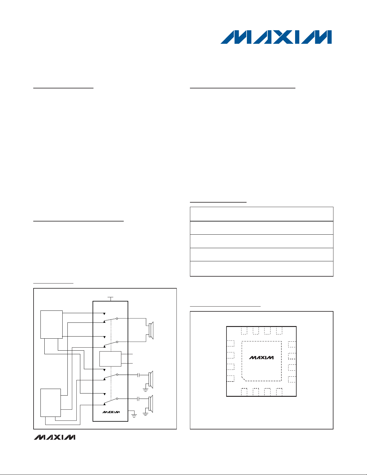
Pin Configuration
Ordering Information
INTERNAL
SPEAKER
GND
EXTERNAL
HEADPHONES
EXTERNAL
HEADPHONES
BLOCKING CAPS
MIDI
(RINGER)
NC1
NC2
NC3
NC4
NO4
NO3
NO2
NO1
COM1
COM2
COM3
COM4
V
CC
1.6V to 5.5V
CB1
CB2
BASEBAND
(SPEECH)
CONTROL
LOGIC
MAX4740
Typical Operating Circuit
PART PIN-PACKAGE
TOP
PKG
CODE
MAX4740ETE+
16 TQFN-EP
(3mm x 3mm)
AEV
T1633-4
MAX4740EVE+
V162A2-1
MAX4740HETE+
16 TQFN-EP
(3mm x 3mm)
AEW
T1633-4
MAX4740HEVE+
V162A2-1
Note: All devices are guaranteed over the -40°C to +85°C
temperature range.
EP = Exposed pad.
MARK
16 Ultra-Thin QFN
(2.5mm x 2.5mm)
16 Ultra-Thin QFN
(2.5mm x 2.5mm)
+AAA
+AAB
TOP VIEW
COM4
NO4
CB2
NC3
12 11 10 9
*CONNECT EP TO GND OR LEAVE EP UNCONNECTED.
NC4
13
V
CC
14
MAX4740
NO1
15
COM1
16
+
2.5mm x 2.5mm Ultra-Thin QFN
MAX4740H
1234
CB1
NC1
3mm x 3mm Thin QFN/
NO2
*EP
COM2
COM3
8
NO3
7
GND
6
5
NC2
MAX4740/MAX4740H
Quad SPDT Audio Switches
2 _______________________________________________________________________________________
ABSOLUTE MAXIMUM RATINGS
Stresses beyond those listed under “Absolute Maximum Ratings” may cause permanent damage to the device. These are stress ratings only, and functional
operation of the device at these or any other conditions beyond those indicated in the operational sections of the specifications is not implied. Exposure to
absolute maximum rating conditions for extended periods may affect device reliability.
(All voltages referenced to GND.)
V
CC
, CB_ ...............................................................-0.3V to +6.0V
COM_, NC_, NO_ .......................................-0.3V to (V
CC
+ 0.3V)
Continuous Current NO_, NC_, COM_ ..........................±300mA
Peak Current NO_, NC_, COM_
(pulsed at 1ms, 50% duty cycle).................................±400mA
Peak Current NO_, NC_, COM_
(pulsed at 1ms, 10% duty cycle).................................±500mA
Continuous Power Dissipation (T
A
= +70°C)
16-Pin TQFN (3mm x 3mm), Single-Layer Board
(derate 15.6mW/°C above +70°C)..............................1250mW
16-Pin TQFN (3mm x 3mm), Multilayer Board (derate
20.8mW/°C above +70°C) ..........................................1667mW
16-Pin Ultra-Thin QFN (2.5mm x 2.5mm), MultiLayer
Board (derate 11.5mW/°C above +70°C) .................923.8mW
Operating Temperature Range ...........................-40°C to +85°C
Junction Temperature......................................................+150°C
Storage Temperature Range .............................-65°C to +150°C
Lead Temperature (soldering, 10s) .................................+300°C
ELECTRICAL CHARACTERISTICS
(VCC= +2.7V to +5.5V, TA= -40°C to +85°C, unless otherwise noted. Typical values are at TA= +25°C, VCC= +3.3V.) (Note 1)
PARAMETER
CONDITIONS
POWER SUPPLY
Supply Voltage Range V
CC
1.6 5.5 V
VCC = +5.5V, VCB_ = 0V or V
CC
0.3 1
VCC = +5.5V, VCB_ = 0.5V or +1.6V 0.3 5
Supply Current I
CC
VCC = +2.5V, VCB_ = 0.5V or +1.4V 0.1
µA
ANALOG SWITCH
Analog Signal Range
V
NC
_,
V
NO
_,
(Note 2) 0
V
TA = +25°C
On-Resistance R
ON
VCC = 3.3V, I
COM_
=
100mA; CB_ = low or
high
T
A
= T
MIN
to
T
MAX
1
Ω
TA = +25°C
On-Resistance Match Between
Channels
ΔR
ON
VCC = 3.3V, VNC_ or
V
NO
_ = 0.875V; I
COM_
=
100mA (Note 3)
T
A
= T
MIN
to
T
MAX
0.1
Ω
TA = +25°C
On-Resistance Flatness
)
VCC = 3.3V, V
COM_
= 0
to V
CC
; I
COM_
= 100mA
(Note 4)
T
A
= T
MIN
to
T
MAX
Ω
NO_, NC_ Off-Leakage Current
(
),
)
VCC = 5.5V; VNC_ or VNO_ = 0.3V, 5.5V;
V
COM
_ = 5.5V or 0.3V
-1 0.1 +1 µA
COM_ On-Leakage Current
(ON)
VCC = 5.5V, VNC_ or VNO_ = 0.3V, 5.5V, or
unconnected; V
COM
_ = 0.3V, 5.5V, or
unconnected
-1 0.1 +1 µA
SYMBOL
MIN TYP MAX UNITS
V
_,
COM
R
FLAT(NO
INO_
OFF
I
NC_(OFF
I
_
COM
0.61 0.90
0.06
0.32 0.72
V
CC
0.87
MAX4740/MAX4740H
Quad SPDT Audio Switches
_______________________________________________________________________________________ 3
ELECTRICAL CHARACTERISTICS (continued)
(VCC= +2.7V to +5.5V, TA= -40°C to +85°C, unless otherwise noted. Typical values are at TA= +25°C, VCC= 3.3V.) (Note 1)
PARAMETER
CONDITIONS
DYNAMIC CHARACTERISTICS
For N O_, V
N O_
= 1V 70
Turn-On Time t
ON
RL = 32Ω, CL =
35pF, Figure 2
For N C _, V
N C _
= 1V
ns
For N O_, V
N O_
= 1V
Turn-Off Time t
OFF
RL = 32Ω, CL =
35pF, Figure 2
For N C _, V
N C _
= 1V 55
ns
Charge Injection Q
V
GEN
_ = 0V; R
GEN
= 0Ω; CL = 1nF;
Figure 3
pC
Off-Isolation V
ISO
CL = 5pF; RL = 32Ω; f = 100kHz;
V
COM
_ = 1V
RMS
; Figure 4 (Note 5)
-64 dB
Crosstalk V
CT
CL = 5pF; RL = 32Ω; f = 100kHz;
V
COM
_ = 1V
RMS
; Figure 4
-68 dB
Power-Supply Rejection Ratio PSRR
f = 20kHz, V
COM_
= 1V
RMS, RL
= 50Ω,
C
L
= 5pF
-60 dB
Total Harmonic Distortion THD f = 20Hz to 20kHz, V
P-P
= 0.5V, RL = 32Ω
%
NO_, NC_ Off-Capacitance
)
(
)
f = 1MHz, Figure 5 40 pF
COM_ On-Capacitance
(ON)
f = 1MHz, Figure 5
pF
DIGITAL INPUTS (CB_)
VCC = 1.6V to 2.7V 1.4
Input Logic-High V
IH
VCC = 2.7V to 5.5V 1.6
V
Input Logic-Low V
IL
0.5 V
Input Leakage Current I
IN
-1 0.1 +1 µA
Note 1: For TQFN (3mm x 3mm) electrical specifications are production tested at TA= +85°C and guaranteed by design at TA= +25°C
and -40°C. For Ultra-Thin QFN (2.5mm x 2.5mm) electrical specifications are production tested at T
A
= +25°C and guaranteed by
design at T
A
= +85°C and -40°C.
Note 2: Signals on COM_, NO_, or NC_ exceeding V
CC
are clamped by internal diodes. Limit forward-diode current to maximum
current rating.
Note 3: ΔR
ON
= R
ON(MAX)
- R
ON(MIN)
.
Note 4: Flatness is defined as the difference between the maximum and minimum value of on-resistance as measured over the
specified analog signal ranges.
Note 5: Off-isolation = 20log10 [V
COM_
/ V
NO_
], V
COM_
= output, V
NO_
= input to off switch.
SYMBOL
C
NC_(OFF
C
_
NO
C
_
COM
,
OFF
MIN TYP MAX UNITS
210
210
200
0.08
150
MAX4740/MAX4740H
Quad SPDT Audio Switches
4 _______________________________________________________________________________________
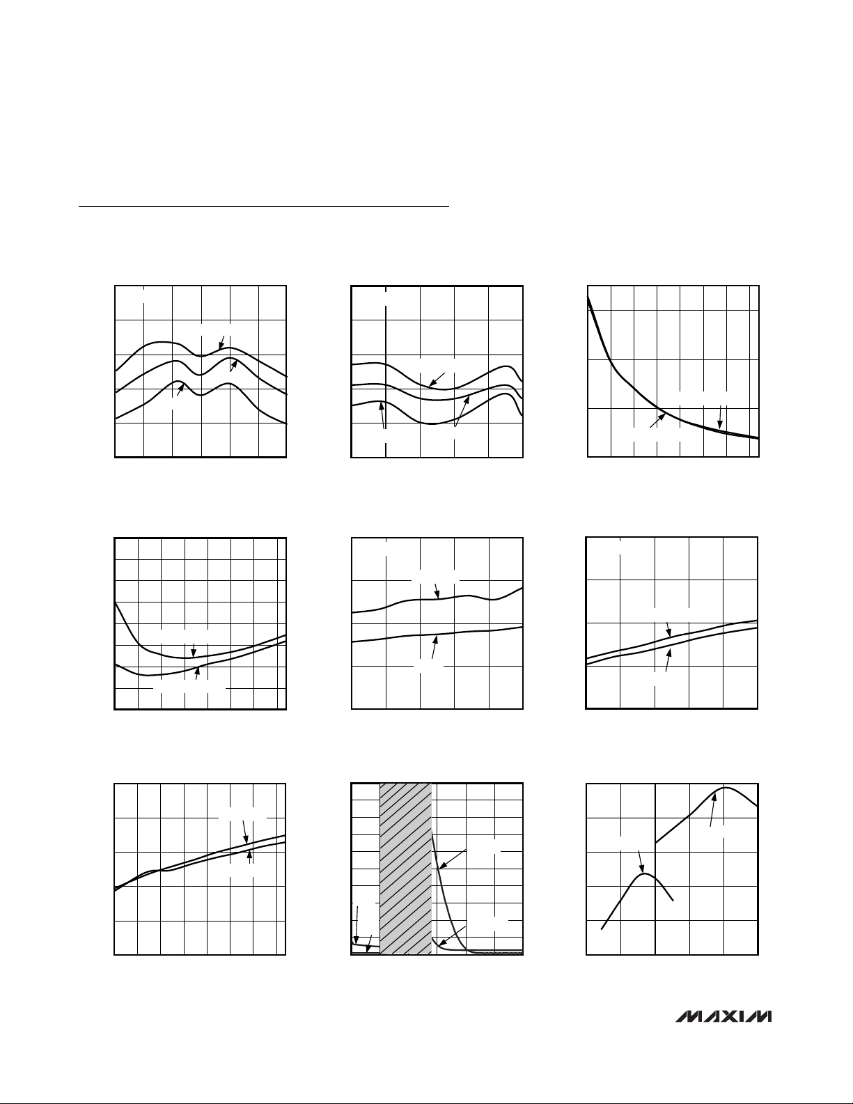
Typical Operating Characteristics
(VCC= 3.3V, TA= +25°C, unless otherwise noted)
0.2
0.3
0.5
0.4
0.6
0.7
0 1.00.5 1.5 2.0 2.5 3.0
ON-RESISTANCE
vs. COM VOLTAGE
MAX4740/40H toc01
COM VOLTAGE (V)
ON-RESISTANCE (Ω)
VCC = 3V
TA = +85°C
TA = +25°C
TA = -40°C
0.1
0.2
0.4
0.3
0.5
0.6
021345
ON-RESISTANCE
vs. COM VOLTAGE
MAX4740/40H toc02
COM VOLTAGE (V)
ON-RESISTANCE (Ω)
TA = +85°C
TA = +25°C
TA = -40°C
VCC = 5V
0
200
400
600
1.8 2.8 3.8 4.82.3 3.3 4.3 5.3
NC TURN-ON/NO TURN-OFF TIME
vs. SUPPLY VOLTAGE
MAX4740/40H toc03
SUPPLY VOLTAGE (V)
TIME (ns)
NC TURN-ON TIME
NO TURN-OFF TIME
20
60
40
100
80
120
140
160
180
1.8 2.8 3.32.3 3.8 4.3 4.8 5.3
NO TURN-ON/NC TURN-OFF TIME
vs. SUPPLY VOLTAGE
MAX4740/40H toc04
SUPPLY VOLTAGE (V)
TURN-ON/TURN-OFF TIME (ns)
NC TURN-OFF TIME
NO TURN-ON TIME
NO TURN-ON/NC TURN-OFF TIME
vs. TEMPERATURE
MAX4740/40H toc05
TEMPERATURE (°C)
TURN-ON/TURN-OFF TIME (ns)
603510-15
40
60
80
100
20
-40 85
VCC = 3V
NO t
ON
NC t
OFF
NC TURN-ON/NO TURN-OFF TIME
vs. TEMPERATURE
MAX4740/40H toc06
TEMPERATURE (°C)
TURN-ON/TURN-OFF TIME (ns)
603510-15
200
300
400
500
100
-40 85
VCC = 3V
NC t
ON
NO t
OFF
0
0.4
1.2
0.8
1.6
2.0
1.8 2.8 3.32.3 3.8 4.3 4.8 5.3
LOGIC THRESHOLD
vs. SUPPLY VOLTAGE
MAX4740/40H toc07
SUPPLY VOLTAGE (V)
LOGIC THRESHOLD (V)
VCB RISING
VCB FALLING
0
20
10
40
30
90
50
100
0 1.0 1.50.5 2.0 2.5 3.0
SUPPLY CURRENT
vs. LOGIC INPUT VOLTAGE
MAX4740/40H toc08
LOGIC INPUT VOLTAGE (V)
SUPPLY CURRENT (nA)
VCC =
3V
VCC =
2.5V
VCC = 3V
VCC = 2.5V
1.4
80
70
60
0
50
150
100
200
250
021345
CHARGE INJECTION
vs. COM VOLTAGE
MAX4740/40H toc09
V
COM
(V)
CHARGE INJECTION ( pC)
VCC = 2.0V
VCC = 5.0V

MAX4740/MAX4740H
Quad SPDT Audio Switches
_______________________________________________________________________________________ 5
Typical Operating Characteristics (continued)
(VCC= 3.3V, TA= +25°C, unless otherwise noted)
0.1
10
1
1000
100
10,000
100,000
-40 10-15 35 60 85
LEAKAGE CURRENT
vs. TEMPERATURE
MAX4740/40H toc10
TEMPERATURE (°C)
LEAKAGE CURRENT (pA)
I
COM(OFF)
I
COM(ON)
OFF-ISOLATION vs. FREQUENCY
MAX4740/40H toc12
FREQUENCY (MHz)
OFF-ISOLATION (dB)
10.10.01
-60
-40
-20
0
-80
0.001 10
TOTAL HARMONIC DISTORTION
vs. FREQUENCY
MAX4740/40H toc14
FREQUENCY (Hz)
THD (%)
10k1k100
0.1
10 100k
1
0.01
RL = 32Ω
FREQUENCY RESPONSE
MAX4740/40H toc11
FREQUENCY (MHz)
ON-LOSS (dB)
1010.1
-4
-2
0
-6
0.01 100
CROSSTALK vs. FREQUENCY
MAX4740/40H toc13
FREQUENCY (MHz)
CROSSTALK (dB)
10.10.01
-60
-40
-20
0
-80
0.001 10
POWER-SUPPLY REJECTION
RATIO vs. FREQUENCY
MAX4740/40H toc15
FREQUENCY (MHz)
PSRR (dB)
10.10.01
10
20
30
40
50
60
70
0
0.001 10

MAX4740/MAX4740H
Detailed Description
The MAX4740/MAX4740H quad SPDT audio switches
are low on-resistance, low supply current, high powersupply rejection ratio (PSRR) devices that operate from
a +1.6V to +5.5V single supply. The MAX4740/
MAX4740H have two digital control inputs, CB1 and
CB2, where each bit controls a pair of switches (see
Tables 1 and 2).
Applications Information
The MAX4740/MAX4740H logic inputs accept up to
+5.5V, regardless of supply voltage. For example with a
+3.3V supply, CB1 and CB2 can be driven low to GND
and high to +5.5V, allowing for mixed logic levels in a
system. Driving CB1 and CB2 rail-to-rail minimizes
power consumption. For a 3.3V supply voltage, the
logic thresholds are +0.5V (low) and +1.6V (high).
Analog Signal Levels
Analog signals that range over the entire supply voltage
range (VCCto GND) can be passed with very little
change in on-resistance (see the
Typical Operating
Characteristics
). The switches are bidirectional, so the
NO_, NC_, and COM_ terminals can be used as either
inputs or outputs.
Quad SPDT Audio Switches
6 _______________________________________________________________________________________
Pin Description
PIN NAME FUNCTION
1 NC1 Analog Switch 1—Normally Closed Terminal
2 CB1 Digital Control Input for Analog Switch 1 and Analog Switch 2
3 NO2 Analog Switch 2—Normally Open Terminal
4 COM2 Analog Switch 2—Common Terminal
5 NC2 Analog Switch 2—Normally Closed Terminal
6 GND Ground
7 NO3 Analog Switch 3—Normally Open Terminal
8 COM3 Analog Switch 3—Common Terminal
9 NC3 Analog Switch 3—Normally Closed Terminal
10 CB2 Digital Control Input for Analog Switch 3 and Analog Switch 4
11 NO4 Analog Switch 4—Normally Open Terminal
12 COM4 Analog Switch 4—Common Terminal
13 NC4 Analog Switch 4—Normally Closed Terminal
14 V
CC
Positive Supply Voltage
15 NO1 Analog Switch 1—Normally Open Terminal
16 COM1 Analog Switch 1—Common Terminal
EP EP Exposed Pad. Connect to GND or leave unconnected for normal operation.
CONTROL SWITCH STATE
CB2 CB1 Switch 3/4 Switch 1/2
0 0 COM = NC COM = NC
0 1 COM = NC COM = NO
1 0 COM = NO COM = NC
1 1 COM = NO COM = NO
Table 1. MAX4740 Truth Table
CONTROL SWITCH STATE
CB2 CB1 Switch 3/4 Switch 1/2
0 0 COM = NC COM = NC
0 1 High-Z High-Z
1 0 COM = NO COM = NC
1 1 COM = NO COM = NO
Table 2. MAX4740H Truth Table

Power-Supply Sequencing and Overvoltage
Protection
Caution: Do not exceed the Absolute Maximum
Ratings since stresses beyond the listed ratings
may cause permanent damage to the device.
Proper power-supply sequencing is recommended for
all CMOS devices. Improper supply sequencing can
force the switch into latch-up, causing it to draw excessive supply current. The only way out of latch-up is to
recycle the power and reapply properly. Connect all
ground pins first, then apply power to V
CC
, and finally
apply signals to NO_, NC_, and COM_. Follow the
reverse order upon power-down.
Chip Information
PROCESS: BICMOS
MAX4740/MAX4740H
Quad SPDT Audio Switches
_______________________________________________________________________________________ 7
CB1
CB2
GND
NC1
COM1
COM2
NO1
NO2
NC2
CONTROL
LOGIC
V
CC
MAX4740
SWITCH 1
SWITCH 2
NC3
COM3
NO3
NC4
COM4
NO4
CB1
CB2
GND
NC1
COM1
COM2
NO1
NO2
NC2
CONTROL
LOGIC
V
CC
MAX4740H
NC3
COM3
NO3
NC4
COM4
NO4
Hi Z
Hi Z
SWITCH 3
SWITCH 4
SWITCH 1
SWITCH 2
SWITCH 3
SWITCH 4
Hi Z
Hi Z
Figure 1. Functional Diagram
tr < 5ns
tf < 5ns
50%
0V
LOGIC
INPUT
R
L
COM_
GND
CB_
C
L
INCLUDES FIXTURE AND STRAY CAPACITANCE.
V
NC_
OR VNO_
V
CC
t
OFF
0V
NO_
OR NC_
0.8 x V
0UT
0.8 x V
OUT
t
ON
V
OUT
SWITCH
OUTPUT
LOGIC
INPUT
CB DEPENDS ON SWITCH CONFIGURATION;
INPUT POLARITY DETERMINED BY SENSE OF SWITCH.
V
CC
C
L
V
CC
V
OUT
MAX4740
MAX4740H
Figure 2. Switching Time
Test Circuits/Timing Diagrams

MAX4740/MAX4740H
Quad SPDT Audio Switches
8 _______________________________________________________________________________________
V
GEN
GND
COM_
C
L
V
OUT
V
CC
V
OUT
CB_
OFF
ON
OFF
ΔV
OUT
Q = (ΔV
OUT
)(CL)
NC_
LOGIC INPUT WAVEFORMS INVERTED FOR SWITCHES
THAT HAVE THE OPPOSITE LOGIC SENSE.
OFF
ON
OFF
CB_
V
IL
TO V
IH
V
CC
R
GEN
CB_
OR NO_
MAX4740
MAX4740H
Figure 3. Charge injection
V
CC
GND
V
CC
COM_
NO_
MEASUREMENTS ARE STANDARDIZED AGAINST SHORT AND OPEN AT SOCKET TERMINALS.
OFF-ISOLATION IS MEASURED BETWEEN COM_ AND OFF NO_ OR NC_ TERMINALS.
ON-LOSS IS MEASURED BETWEEN COM_ AND ON NO_ OR NC_ TERMINAL ON EACH SWITCH.
CROSSTALK IS MEASURED FROM ONE CHANNEL TO THE OTHER CHANNEL.
SIGNAL DIRECTION THROUGH SWITCH IS REVERSED; WORST VALUES ARE RECORDED.
NC_
1μF
V
IN
V
OUT
NETWORK
ANALYZER
50Ω 50Ω
50Ω 50Ω
MEAS REF
MAX4740
MAX4740H
CB_
0V OR
V
CC
OFF-ISOLATION = 20log
OFF-LOSS = 20log
CROSSTALK = 20log
V
IN
V
OUT
V
IN
V
OUT
V
IN
V
OUT
50Ω
Figure 4. Off-Isolation, On-Loss, and Crosstalk
Test Circuits/Timing Diagrams (continued)

MAX4740/MAX4740H
Quad SPDT Audio Switches
_______________________________________________________________________________________ 9
GND
V
IL
OR V
IH
NC_ OR
NO_
COM_
MAX4740
MAX4740H
V
CC
CAPACITANCE
ANALYZER
CB_
1μF
f = 1MHz
Figure 5. Channel Off/On-Capacitance

MAX4740/MAX4740H
Quad SPDT Audio Switches
10 ______________________________________________________________________________________
Package Information
(The package drawing(s) in this data sheet may not reflect the most current specifications. For the latest package outline information,
go to www.maxim-ic.com/packages
.)
12, 16L QFN.EPS
G
1
2
21-0102
PACKAGE OUTLINE, 12,16L QFN, 3x3x0.90 MM

MAX4740/MAX4740H
Quad SPDT Audio Switches
______________________________________________________________________________________ 11
Package Information (continued)
(The package drawing(s) in this data sheet may not reflect the most current specifications. For the latest package outline information,
go to www.maxim-ic.com/packages
.)
G
1
2
21-0102
PACKAGE OUTLINE, 12,16L QFN, 3x3x0.90 MM

MAX4740/MAX4740H
Quad SPDT Audio Switches
12 ______________________________________________________________________________________
Package Information (continued)
(The package drawing(s) in this data sheet may not reflect the most current specifications. For the latest package outline information,
go to www.maxim-ic.com/packages
.)
ULTRA THIN QFN.EPS
DETAIL A
DETAIL B
DETAIL B
DETAIL A

MAX4740/MAX4740H
Quad SPDT Audio Switches
Maxim cannot assume responsibility for use of any circuitry other than circuitry entirely embodied in a Maxim product. No circuit patent licenses are
implied. Maxim reserves the right to change the circuitry and specifications without notice at any time.
Maxim Integrated Products, 120 San Gabriel Drive, Sunnyvale, CA 94086 408-737-7600 ____________________
13
© 2007 Maxim Integrated Products is a registered trademark of Maxim Integrated Products, Inc.
Boblet
Revision History
REVISION
NUMBER
REVISION
DATE
DESCRIPTION
PAGES
CHANGED
0 5/06 Initial release —
1 11/07 Adding ultra-thin QFN package 1, 2, 3, 10–13
 Loading...