


General Description
The MAX4736 is a low on-resistance, low-voltage, dual
single-pole/double throw (SPDT) analog switch that
operates from a single 1.6V to 4.2V supply. This device
has fast switching speeds (tON= 25ns, t
OFF
= 20ns
max), handles rail-to-rail analog signals, and consumes
less than 4µW of quiescent power. The MAX4736 has
break-before-make switching.
When powered from a 3V supply, the MAX4736 features low 0.6Ω on-resistance (RON), with 0.1Ω R
ON
matching and 0.05Ω RONflatness. The digital logic
input is 1.8V CMOS compatible when using a single 3V
supply.
The MAX4736 has one normally open (NO) switch and
one normally closed (NC) switch, and is available in 12pin TQFN-EP (3mm x 3mm), 10-pin µMAX and 10 pin
µDFN (2mm x 2mm) packages.
Applications
Power Routing
Battery-Powered Systems
Audio and Video Signal Routing
Low-Voltage Data-Acquisition Systems
Communications Circuits
PCMCIA Cards
Cellular Phones
Modems
Hard Drives
Features
♦ Low R
ON
0.6Ω (3V Supply)
1.5Ω (1.8V Supply)
♦ 0.1Ω max RONFlatness (3V Supply)
♦ Single-Supply Operation Down to 1.6V
♦ Available in TQFN, µDFN and µMAX Packages
♦ 1.8V CMOS Logic Compatible (3V Supply)
♦ Fast Switching: t
ON
= 25ns, t
OFF
= 20ns
MAX4736
0.6Ω, Low-Voltage, Single-Supply, Dual SPDT
Analog Switch
________________________________________________________________ Maxim Integrated Products 1
TOP VIEW
MAX4736
MAX4736
IN_
NO_
NC_
0
OFF
ON
1
ON
OFF
SWITCHES SHOWN
FOR LOGIC 0 INPUT
1
2
3
4
5
10
9
8
7
6
NO2
GND
NO1
IN1
µMAX/µDFN
IN2
NC2
V+
NC1
COM1
COM2
12
IN111COM110N.C.
9 NC1
8 V+
7 NC2
4
IN25COM26N.C.
1NO1
2GND
3NO2
MAX4736
TQFN
NOTE: CONNECT EXPOSED PAD ON
TQFN AND µDFN TO GND.
Pin Configurations/Functional Diagrams/Truth Table
Ordering Information
Note: All devices operate over the -40°C to +55°C operating
temperature range.
*EP = Exposed pad.
19-2382; Rev 2; 12/06
For pricing, delivery, and ordering information, please contact Maxim/Dallas Direct! at
1-888-629-4642, or visit Maxim’s website at www.maxim-ic.com.
PART PIN-PACKAGE PKG CODE
MAX4736EUB 10 µMAX U10-2
MAX4736ETC
T1233-1
MAX4736ELB 10 µDFN L1022-1
12 Thin QFN-EP*
MAX4736
0.6Ω, Low-Voltage, Single-Supply, Dual SPDT
Analog Switch
2 _______________________________________________________________________________________
ABSOLUTE MAXIMUM RATINGS
ELECTRICAL CHARACTERISTICS—Single 3V Supply
(V+ = 2.7V to 4.2V, VIH= 1.4V, VIL= 0.5V, TA= T
MIN
to T
MAX
, unless otherwise specified. Typical values are at V+ = 3.0V,
T
A
= +25°C.) (Notes 2, 3)
Stresses beyond those listed under “Absolute Maximum Ratings” may cause permanent damage to the device. These are stress ratings only, and functional
operation of the device at these or any other conditions beyond those indicated in the operational sections of the specifications is not implied. Exposure to
absolute maximum rating conditions for extended periods may affect device reliability.
Note 1: Signals on COM_, NO_, or NC_ exceeding V+ or GND are clamped by internal diodes. Limit forward current to maximum
current rating.
(Voltages referenced to GND.)
V+, IN_...................................................................-0.3V to +4.6V
COM_, NO_, NC_ (Note 1) ...........................-0.3V to (V+ + 0.3V)
Continuous Current COM_, NO_, NC_ ...........................±300mA
Continuous Current (all other pins)...................................±20mA
Peak Current COM_, NO_, NC_
(pulsed at 1ms 10% duty cycle)...................................±500mA
Continuous Power Dissipation (T
A
= +70°C)
10-Pin µDFN (derate 5.3mW/°C above +70°C) ..........423.7mW
10-Pin µMAX (derate 5.6mW/°C above +70°C) .............444mW
12-Pin TQFN-EP (derate 14.7mW/°C above +70°C)....1176mW
Operating Temperature Range ...........................-40°C to +85°C
Maximum Junction Temperature .....................................+150°C
Storage Temperature Range .............................-65°C to +150°C
Lead Temperature (soldering, 10s) .................................+300°C
PARAMETER
UNITS
ANALOG SWITCH
Analog Signal Range
VNO_,
V
NC
_
0V+V
+25°C 0.6 0.8
On-Resistance (Note 4) R
ON
V + = 2.7V ,
I
C OM
_ = 100m A;
V
NO
_ or VNC_ = 1.5V
1
Ω
+25°C 0.1 0.2
On-Resistance Match
Between Channels
(Notes 4, 5)
∆R
ON
V + = 2.7V ,
I
C OM
_ = 100mA;
V
NO
_ or VNC_ = 1.5V
0.3
Ω
+25°C
0.1
On-Resistance Flatness
(Note 6)
)
V+ = 2.7V,
I
COM
_ = 100m A;
0.2
Ω
+25°C -1
+1
NO_ or NC_ Off-Leakage
Current
(Note 10)
),
)
V + = 3.6V ,
V
C OM
_ = 0.3V, 3.3V;
V
NO
_ or VNC_ = 3.3V, 0.3V
-5 +5
nA
+25°C -2
+2
COM_ On-Leakage Current
(Note 10)
)
V+ = 3.6V,
V
C OM
_ = 0.3V, 3.3V;
V
NO
_ or VNC_ = 0.3V, 3.3V, or
floating
-10
nA
SYMBOL CONDITIONS T
A
MIN TYP MAX
V
_,
COM
T
to T
MIN
MAX
T
to T
MIN
MAX
0.05
R
FLAT(ON
VNO_ or VNC_ = 1V, 1.5V, 2V
INO_
(OFF
INC_
(OFF
I
COM_(ON
T
to T
MIN
MAX
T
to T
MIN
MAX
±0.002
±0.002
T
MIN
to T
MAX
+10
MAX4736
0.6Ω, Low-Voltage, Single-Supply, Dual SPDT
Analog Switch
_______________________________________________________________________________________ 3
ELECTRICAL CHARACTERISTICS—Single 3V Supply (continued)
(V+ = 2.7V to 4.2V, VIH= 1.4V, VIL= 0.5V, TA= T
MIN
to T
MAX
, unless otherwise specified. Typical values are at V+ = 3.0V,
T
A
= +25°C.) (Notes 2, 3)
PARAMETER
SYMBOL
CONDITIONS
T
A
MIN
TYP
MAX
UNITS
SWITCH DYNAMIC CHARACTERISTICS
+25°C 20 25
Turn-On Time t
ON
VNO_, VNC_ = 1.5V;
R
L
= 50Ω, CL = 35pF,
Figure 1
30
ns
+25°C 15 20
Turn-Off Time t
OFF
VNO_, VNC_ = 1.5V;
R
L
= 50Ω, CL = 35pF,
Figure 1
25
ns
+25°C 5
Break-Before-Make (Note 7) t
BBM
VNO_, VNC_ = 1.5V;
R
L
= 50Ω, CL = 35pF,
Figure 2
1
ns
Charge Injection Q
V
GEN
= 0, R
GEN
= 0,
C
L
= 1.0nF, Figure 3
+25°C 60 pC
NO_ or NC_ Off-Capacitance C
OFF
f = 1MHz, Figure 4 +25°C 33 pF
COM_ Off-Capacitance
)
f = 1MHz, Figure 4 +25°C 60 pF
COM_ On-Capacitance
)
f = 1MHz, Figure 4 +25°C 85 pF
-3dB On-Channel Bandwidth BW
Signal = 0, R
IN
= R
OUT
=
50Ω, C
L
= 5pF, Figure 5
130
MHz
Off-Isolation (Note 8) V
ISO
50Ω, C L = 5p F, Fi g ur e 5
+25°C -52 dB
Crosstalk (Note 9) V
CT
50Ω, C L = 5p F, Fi g ur e 5
+25°C -78 dB
Total Harmonic Distortion THD
f = 20Hz to 20kHz, V
COM
_ =
2V
P-P
, RL = 32Ω
+25°C
%
LOGIC INPUT (A_, IN_)
Input Logic High V
IH
1.4 V
Input Logic Low V
IL
0.5 V
Input Leakage Current I
IN
V
IN_
= 0 or 3.6V -1
+1 µA
POWER SUPPLY
Power-Supply Range V+ 1.6 3.6 V
Positive Supply Current I+
V+ = 3.6V, V
IN
_ = 0 or V+,
all channels on or off
1µA
C
COM(OFF
C
COM(ON
f = 1M H z, V
f = 1M H z, V
T
to T
MIN
MAX
T
to T
MIN
MAX
T
to T
MIN
MAX
COM
COM
_ = 1V
_ = 1V
, RL =
P - P
, RL =
P - P
0.018
+0.005
0.006
MAX4736
0.6Ω, Low-Voltage, Single-Supply, Dual SPDT
Analog Switch
4 _______________________________________________________________________________________
ELECTRICAL CHARACTERISTICS—Single 1.8V Supply
(V+ = 1.8V, VIH= 1.0V, VIL= 0.4V, TA= T
MIN
to T
MAX
, unless otherwise specified. Typical values are at TA= +25°C.) (Notes 2, 3)
PARAMETER
CONDITIONS T
A
UNITS
ANALOG SWITCH
Analog Signal Range
0V+V
+25°C 1.5 2
On-Resistance R
ON
I
COM
_ = 10mA;
V
NO
_ or VNC_ = 1V
3
Ω
SWITCH DYNAMIC CHARACTERISTICS
+25°C 25 30
Turn-On Time t
ON
VNO_ or VNC_ = 1V;
RL = 50Ω, C
L
= 35pF,
Figure 1
35
ns
+25°C 18 25
Turn-Off Time t
OFF
VNO_ or VNC_ = 1V;
R
L
= 50Ω, CL = 35pF,
Figure 1
28
ns
+25°C 7
Break-Before-Make (Note 7) t
BBM
VNO_ or VNC_ = 1V;
R
L
= 50Ω, CL = 35pF,
Figure 2
1
ns
Charge Injection Q
V
GEN
= 0, R
GEN
= 0,
C
L
= 1nF, Figure 3
+25°C 35 pC
Off-Isolation (Note 8) V
ISO
f = 1M H z, V
N O
_ = VNC_
= 1V
P - P
, RL = 50Ω,
C
L
= 5p F, Fi g ur e 5
+25°C -52 dB
Crosstalk (Note 9) V
CT
f = 1M H z, V
C OM
_ = 1V
P - P
,
+25°C -78 dB
LOGIC INPUT (IN_)
Input Logic High V
IH
1V
Input Logic Low V
IL
0.4 V
Input Leakage Current I
IN
VIN_ = 0 or 3.6V 1 µA
Note 2: The algebraic convention, where the most negative value is a minimum and the most positive value is a maximum, is
used in this data sheet.
Note 3: -40°C specifications are guaranteed by design.
Note 4: R
ON
and ∆RONmatching specifications for QFN packaged parts are guaranteed by design.
Note 5: ∆R
ON
= R
ON(MAX)
- R
ON(MIN)
.
Note 6: Flatness is defined as the difference between the maximum and the minimum value of on-resistance as measured over the
specified analog signal ranges.
Note 7: Guaranteed by design.
Note 8: Off-Isolation = 20log
10(VCOM_/VNO
_), V
COM_
= output, VNO_ = input to OFF switch.
Note 9: Between two switches.
Note 10: Leakage parameters are 100% tested at hot temperature and guaranteed by correlation at room.
Note 11: Devices are guaranteed to 1 million cycles of operation. (Cycle = switch on → switch off → switch on)
Note 12: The minimum load resistance is 8Ω.
SYMBOL
V
_,
COM
_,
V
NO
V
_
NC
MIN TYP MAX
RL = 50Ω, C L = 5p F, Fi g ur e 5
T
to T
MIN
MAX
T
to T
MIN
MAX
T
to T
MIN
MAX
T
to T
MIN
MAX
MAX4736
0.6Ω, Low-Voltage, Single-Supply, Dual SPDT
Analog Switch
_______________________________________________________________________________________ 5
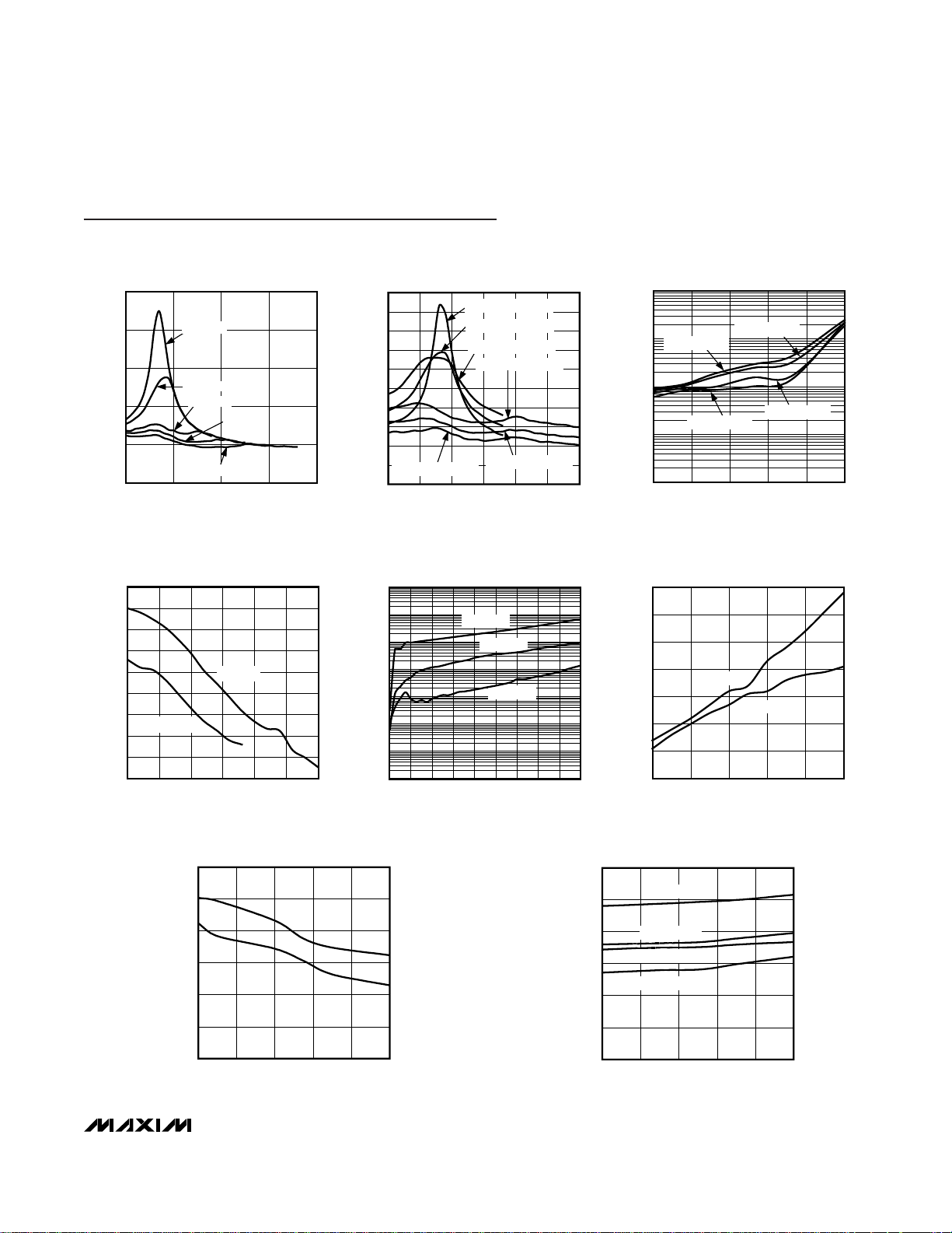
Typical Operating Characteristics
(TA = +25°C, unless otherwise noted.)
ON-RESISTANCE vs. V
COM
MAX4736 toc01
V
COM
(V)
R
ON
(Ω)
0.5
1.0
1.5
2.0
2.5
0
32104
V+ = 3.0V
V+ = 3.6V
V+ = 1.6V
V+ = 1.8V
V+ = 2.5V
MAX4736 toc02
V
COM
(V)
R
ON
(Ω)
2.52.01.51.00.5
0.2
0.4
0.6
0.8
1.0
1.2
1.4
1.6
1.8
2.0
0
0 3.0
ON-RESISTANCE
vs. V
COM
AND TEMPERATURE
V+ = 1.8V, TA = -40°C
V+ = 1.8V, TA = +85°C
V+ = 3.0V, TA = +85°C
V+ = 1.8V, TA = +25°C
V+ = 3.0V, TA = +25°C
V+ = 3.0V, TA = -40°C
ON/OFF-LEAKAGE CURRENT
vs. TEMPERATURE
MAX4736 toc03
TEMPERATURE (°C)
LEAKAGE CURRENT (pA)
603510-15
10
100
1000
10,000
1
-40 85
OFF, V+ = 3.0V
ON, V+ = 3.0V
ON, V+ = 1.8V
OFF, V+ = 1.8V
-20
0
-10
30
20
10
60
50
40
70
0 1.00.5 2.0 2.5 3.0
CHARGE INJECTION vs. V
COM
MAX4736 toc04
V
COM
(V)
Q (pC)
V+ = 3.0V
V+ = 1.8V
1.5
1000
0.0001
0 0.4 2.0 2.8
SUPPLY CURRENT vs. SUPPLY
VOLTAGE AND TEMPERATURE
0.001
1
100
MAX4736 toc05
SUPPLY VOLTAGE (V)
SUPPLY CURRENT (nA)
1.6
3.6
10
0.1
0.01
0.8
1.2
3.2
2.4
TA = -40°C
TA = +25°C
TA = +85°C
0.5
0.7
0.6
1.0
0.9
0.8
1.1
1.2
2.42.0 2.8 3.2 3.6
LOGIC-LEVEL THRESHOLD
vs. SUPPLY VOLTAGE
MAX4736 toc06
SUPPLY VOLTAGE (V)
THRESHOLD (V)
1.6
RISING
FALLING
TURN-ON/OFF TIME
vs. SUPPLY VOLTAGE
MAX4736 toc07
SUPPLY VOLTAGE (V)
t
ON
/t
OFF
(ns)
3.22.82.42.0
5
10
15
20
25
30
0
1.6 3.6
t
OFF
t
ON
TURN-ON/OFF TIMES
vs. TEMPERATURE
MAX4736 toc08
TEMPERATURE (°C)
t
ON
/t
OFF
(ns)
603510-15
5
10
15
20
25
30
0
-40 85
tON, V+ = 1.8V
t
OFF
, V+ = 1.8V
tON, V+ = 3.0V
t
OFF
, V+ = 3.0V

MAX4736
0.6Ω, Low-Voltage, Single-Supply, Dual SPDT
Analog Switch
6 _______________________________________________________________________________________
Typical Operating Characteristics (continued)
(TA = +25°C, unless otherwise noted.)
10 100 1k 10k
TOTAL HARMONIC DISTORTION
vs. FREQUENCY
MAX4736 toc10
FREQUENCY (Hz)
THD (%)
100k
RL = 32
Ω
0.02
0.04
0.06
0.08
0.10
0
V+ = 3.0V
V
COM
= 2V
P-P
V+ = 1.8V
V
COM
= 1.2V
P-P
Pin Description
PIN
µMAX/µDFN
TQFN
NAME FUNCTION
1 12 IN1 Digital Control Input Switch 1
2 1 NO1 Analog Switch 1—Normally Open Terminal
3 2 GND Ground
4 3 NO2 Analog Switch 2—Normally Open Terminal
5 4 IN2 Digital Control Input Switch 2
6 5 COM2 Analog Switch 2—Common Terminal
7 7 NC2 Analog Switch 2—Normally Closed Terminal
8 8 V+ Positive-Supply Voltage Input
9 9 NC1 Analog Switch 1—Normally Closed Terminal
10 11 COM1 Analog Switch 1—Common Terminal
— 6, 10 N.C. No Connection
— EP EP Exposed Pad. Connect to ground.
LOSS (dB)
15
FREQUENCY RESPONSE
0
-15
-30
-45
-60
-75
-90
-105
-120
0.01 100 1000
ON-RESPONSE
OFF-ISOLATION
CROSSTALK
0.1 1 10
FREQUENCY (MHz)
MAX4736 toc09

Detailed Description
The MAX4736 is a low 0.8Ω max (at V+ = 2.7V) onresistance, low-voltage, dual SPDT analog switch that
operates from a 1.6V to 4.2V single supply. CMOS
switch construction allows switching analog signals that
range from GND to V+.
When powered from a 2.7V supply, the 0.8Ω max R
ON
allows high continuous currents to be switched in a
variety of applications.
Applications Information
Proper power-supply sequencing is recommended for
all CMOS devices. Do not exceed the absolute maximum ratings; stresses beyond the listed ratings can
cause permanent damage to the devices. Always
sequence V+ on first, followed by NO_, NC_, or COM_.
Although it is not required, power-supply bypassing
improves noise margin and prevents switching noise
propagation from the V+ supply to other components.
A 0.1µF capacitor, connected from V+ to GND, is adequate for most applications.
Logic Inputs
The MAX4736 logic inputs can be driven up to 3.6V,
regardless of the supply voltage. For example, with a 1.8V
supply, IN_ can be driven low to GND and high to 3.6V.
Driving IN_ rail-to-rail minimizes power consumption.
Analog Signal Levels
Analog signals that range over the entire supply voltage
(V+ to GND) can be passed with very little change in onresistance (see Typical Operating Characteristics). The
switches are bidirectional, so the NO_, NC_, and COM_
pins can be used as either inputs or outputs.
Layout
High-speed switches require proper layout and design
procedures for optimum performance. Reduce stray
inductance and capacitance by keeping traces short
and wide. Ensure that bypass capacitors are as close
to the device as possible. Use large ground planes
where possible.
MAX4736
0.6Ω, Low-Voltage, Single-Supply, Dual SPDT
Analog Switch
_______________________________________________________________________________________ 7
tr < 5ns
tf < 5ns
50%
0
V
IN_
= VIH + 0.5V
t
OFF
0
0.9 ✕ V
0UT
0.9 ✕ V
OUT
t
ON
V
OUT
SWITCH
OUTPUT
LOGIC
INPUT
LOGIC INPUT WAVEFORMS INVERTED FOR SWITCHES
THAT HAVE THE OPPOSITE LOGIC SENSE.
MAX4736
LOGIC
INPUT
R
L
GND
C
L
INCLUDES FIXTURE AND STRAY CAPACITANCE.
NO_ or NC_
IN_
NC_ or NO_
V
OUT
V+
V+
C
L
V
IN
COM_
Figure 1. Switching Time
Test Circuits/Timing Diagrams

MAX4736
0.6Ω, Low-Voltage, Single-Supply, Dual SPDT
Analog Switch
8 _______________________________________________________________________________________
50%
VIH + 0.5V
0
LOGIC
INPUT
V
OUT
0.9 ✕ V
OUT
t
D
MAX4736
LOGIC
INPUT
R
L
GND
C
L
INCLUDES FIXTURE AND STRAY CAPACITANCE.
NO_ or NC_
IN_
NC_ or NO_
V
OUT
V+
V+
C
L
V
IN
COM_
tr < 5ns
tf < 5ns
Figure 2. Break-Before-Make Interval
V
GEN
GND
COM_
C
L
V
OUT
V+
V
OUT
IN
OFF
ON
OFF
∆V
OUT
Q = (∆V
OUT
)(CL)
OR NO_
NC_
IN DEPENDS ON SWITCH CONFIGURATION;
INPUT POLARITY DETERMINED BY SENSE OF SWITCH.
OFF
ON
OFF
IN
V
INL
TO V
INH
V+
R
GEN
IN
MAX4736
Figure 3. Charge Injection
Figure 4. Channel Off/On-Capacitance
Test Circuits/Timing Diagrams (continued)
Chip Information
TRANSISTOR COUNT: 379
PROCESS: CMOS
V+
10nF
V+
COM_
CAPACITANCE
METER
f = 1MHz
NC_ OR
NO_
GND
MAX4736
V
INL
IN_
OR
V
INH

MAX4736
0.6Ω, Low-Voltage, Single-Supply, Dual SPDT
Analog Switch
_______________________________________________________________________________________ 9
MEASUREMENTS ARE STANDARDIZED AGAINST SHORTS AT IC TERMINALS.
OFF-ISOLATION IS MEASURED BETWEEN COM_ AND "OFF" NO_ OR NC_ TERMINAL ON EACH SWITCH.
ON-LOSS IS MEASURED BETWEEN COM_ AND "ON" NO_ OR NC_ TERMINAL ON EACH SWITCH.
CROSSTALK IS MEASURED FROM ONE CHANNEL TO ALL OTHER CHANNELS.
SIGNAL DIRECTION THROUGH SWITCH IS REVERSED; WORST VALUES ARE RECORDED.
V+
V
OUT
V+
IN_
NC_
COM_
NO
V
IN
MAX4736
OFF-ISOLATION = 20log
V
OUT
V
REF
ON-LOSS = 20log
V
OUT
V
REF
CROSSTALK = 20log
V
OUT
V
REF
NETWORK
ANALYZER
50
9
50
9
50
9
50
9
MEAS REF
10nF
0 OR V+
50
9
GND
Figure 5. On-Loss, Off-Isolation, and Crosstalk

MAX4736
0.6Ω, Low-Voltage, Single-Supply, Dual SPDT
Analog Switch
10 ______________________________________________________________________________________
6, 8, 10L UDFN.EPS
EVEN TERMINAL
L
C
ODD TERMINAL
L
C
L
e
L
A
e
E
D
PIN 1
INDEX AREA
b
e
A
b
N
SOLDER
MASK
COVERAGE
A A
1
PIN 1
0.10x45∞
L
L1
(N/2 -1) x e)
XXXX
XXXX
XXXX
SAMPLE
MARKING
A1
A2
7
A
1
2
21-0164
PACKAGE OUTLINE,
6, 8, 10L uDFN, 2x2x0.80 mm
-DRAWING NOT TO SCALE-
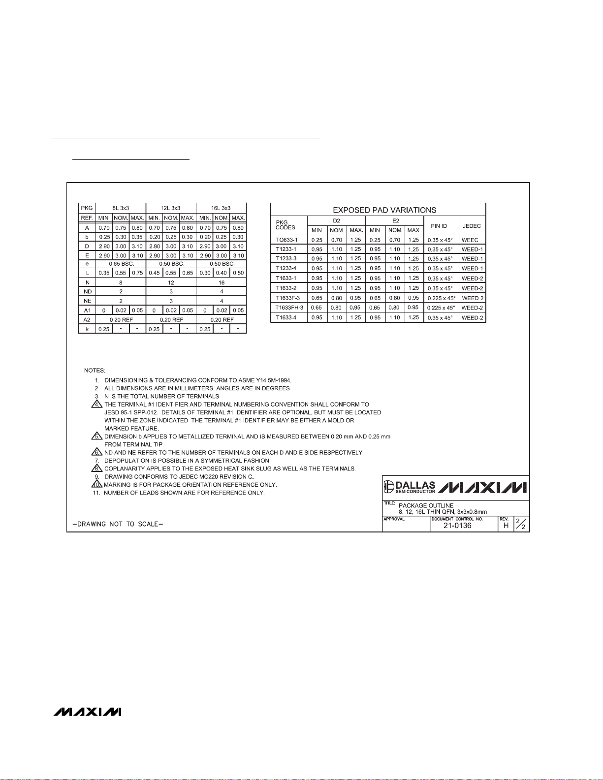
Package Information
(The package drawing(s) in this data sheet may not reflect the most current specifications. For the latest package outline information,
go to www.maxim-ic.com/packages
.)

MAX4736
0.6Ω, Low-Voltage, Single-Supply, Dual SPDT
Analog Switch
______________________________________________________________________________________ 11
Package Information (continued)
(The package drawing(s) in this data sheet may not reflect the most current specifications. For the latest package outline information,
go to www.maxim-ic.com/packages
.)
COMMON DIMENSIONS
SYMBOL MIN. NOM.
A
0.70 0.75
A1
D 1.95 2.00
E
1.95 2.00
L
0.30 0.40
PKG. CODE N e b
PACKAGE VARIATIONS
L1
6L622-1 0.65 BSC 0.30±0.05
0.25±0.050.50 BSC8L822-1
0.20±0.030.40 BSC10L1022-1
2.05
0.80
MAX.
0.50
2.05
0.10 REF.
(N/2 -1) x e
1.60 REF.
1.50 REF.
1.30 REF.
A2
-
-DRAWING NOT TO SCALE-
A
2
2
21-0164
PACKAGE OUTLINE,
6, 8, 10L uDFN, 2x2x0.80 mm
0.15 0.20 0.25
0.020 0.025 0.035

MAX4736
0.6Ω, Low-Voltage, Single-Supply, Dual SPDT
Analog Switch
12 ______________________________________________________________________________________
Package Information (continued)
(The package drawing(s) in this data sheet may not reflect the most current specifications. For the latest package outline information,
go to www.maxim-ic.com/packages
.)
12x16L QFN THIN.EPS
MAX4736
0.6Ω, Low-Voltage, Single-Supply, Dual SPDT
Analog Switch
______________________________________________________________________________________ 13
Package Information (continued)
(The package drawing(s) in this data sheet may not reflect the most current specifications. For the latest package outline information,
go to www.maxim-ic.com/packages
.)
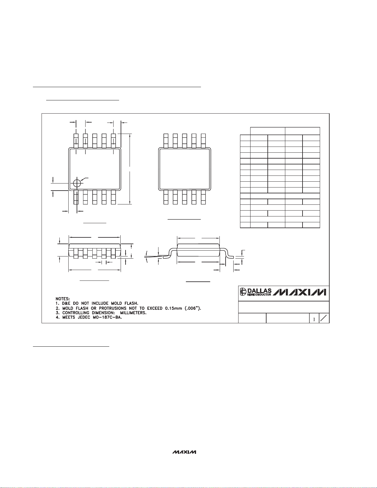
10LUMAX.EPS
PACKAGE OUTLINE, 10L uMAX/uSOP
1
1
21-0061
REV.DOCUMENT CONTROL NO.APPROVAL
PROPRIETARY INFORMATION
TITLE:
TOP VIEW
FRONT VIEW
1
0.498 REF
0.0196 REF
S
6°
SIDE VIEW
α
BOTTOM VIEW
0° 0° 6°
0.037 REF
0.0078
MAX
0.006
0.043
0.118
0.120
0.199
0.0275
0.118
0.0106
0.120
0.0197 BSC
INCHES
1
10
L1
0.0035
0.007
e
c
b
0.187
0.0157
0.114
H
L
E2
DIM
0.116
0.114
0.116
0.002
D2
E1
A1
D1
MIN
-A
0.940 REF
0.500 BSC
0.090
0.177
4.75
2.89
0.40
0.200
0.270
5.05
0.70
3.00
MILLIMETERS
0.05
2.89
2.95
2.95
-
MIN
3.00
3.05
0.15
3.05
MAX
1.10
10
0.6±0.1
0.6±0.1
Ø0.50±0.1
H
4X S
e
D2
D1
b
A2
A
E2
E1
L
L1
c
α
GAGE PLANE
A2 0.030 0.037 0.75 0.95
A1
Package Information (continued)
(The package drawing(s) in this data sheet may not reflect the most current specifications. For the latest package outline information,
go to www.maxim-ic.com/packages
.)
Revision History
Pages changed at Rev 2: 1, 6, 10–14
MAX4736
0.8Ω, Low-Voltage, Single-Supply, Dual SPDT
Analog Switch
Maxim cannot assume responsibility for use of any circuitry other than circuitry entirely embodied in a Maxim product. No circuit patent licenses are
implied. Maxim reserves the right to change the circuitry and specifications without notice at any time.
14 ____________________Maxim Integrated Products, 120 San Gabriel Drive, Sunnyvale, CA 94086 408-737-7600
© 2006 Maxim Integrated Products is a registered trademark of Maxim Integrated Products, Inc.
 Loading...