

Page 1
General Description
The MAX4731/MAX4732/MAX4733 low-voltage, dual,
single-pole/single-throw (SPST) analog switches operate from a single +2V to +11V supply and handle railto-rail analog signals. These switches exhibit low
leakage current (0.1nA) and consume less than 0.5nW
(typ) of quiescent power, making them ideal for batterypowered applications.
When powered from a +3V supply, these switches feature 50Ω (max) on-resistance (RON) with 3.5Ω (max)
matching between channels, and 9Ω (max) flatness
over the specified signal range.
The MAX4731 has two normally open (NO) switches,
the MAX4732 has two normally closed (NC) switches,
and the MAX4733 has one NO and one NC switch. The
MAX4731/MAX4732/MAX4733 are available in 9-bump
chip-scale packages (UCSP™), along with 8-pin TDFN
and 8-pin µMAX®packages. The tiny UCSP occupies a
1.52mm ✕ 1.52mm area and significantly reduces the
required PC board area.
Applications
Battery-Powered Systems
Audio/Video-Signal Routing
Low-Voltage Data-Acquisition Systems
Cell Phones
Communications Circuits
PDAs
Features
♦ 1.52mm ✕ 1.52mm UCSP Package
♦ Guaranteed On-Resistance (RON)
25Ω (max) at +5V
50Ω (max) at +3V
♦ On-Resistance Matching
3Ω (max) at +5V
3.5Ω (max) at +3V
♦ Guaranteed < 0.1nA Leakage Current at
TA= +25°C
♦ Single-Supply Operation from +2.0V to +11V
♦ TTL/CMOS-Logic Compatible
♦ -108dB Crosstalk (1MHz)
♦ -72dB Off-Isolation (1MHz)
♦ Low Power Consumption: 0.5nW (typ)
♦ Rail-to-Rail Signal Handling
MAX4731/MAX4732/MAX4733
50
Ω,
Dual SPST Analog Switches in UCSP
________________________________________________________________ Maxim Integrated Products 1
Ordering Information
19-2645; Rev 2 12/06
For pricing, delivery, and ordering information, please contact Maxim/Dallas Direct! at
1-888-629-4642, or visit Maxim’s website at www.maxim-ic.com.
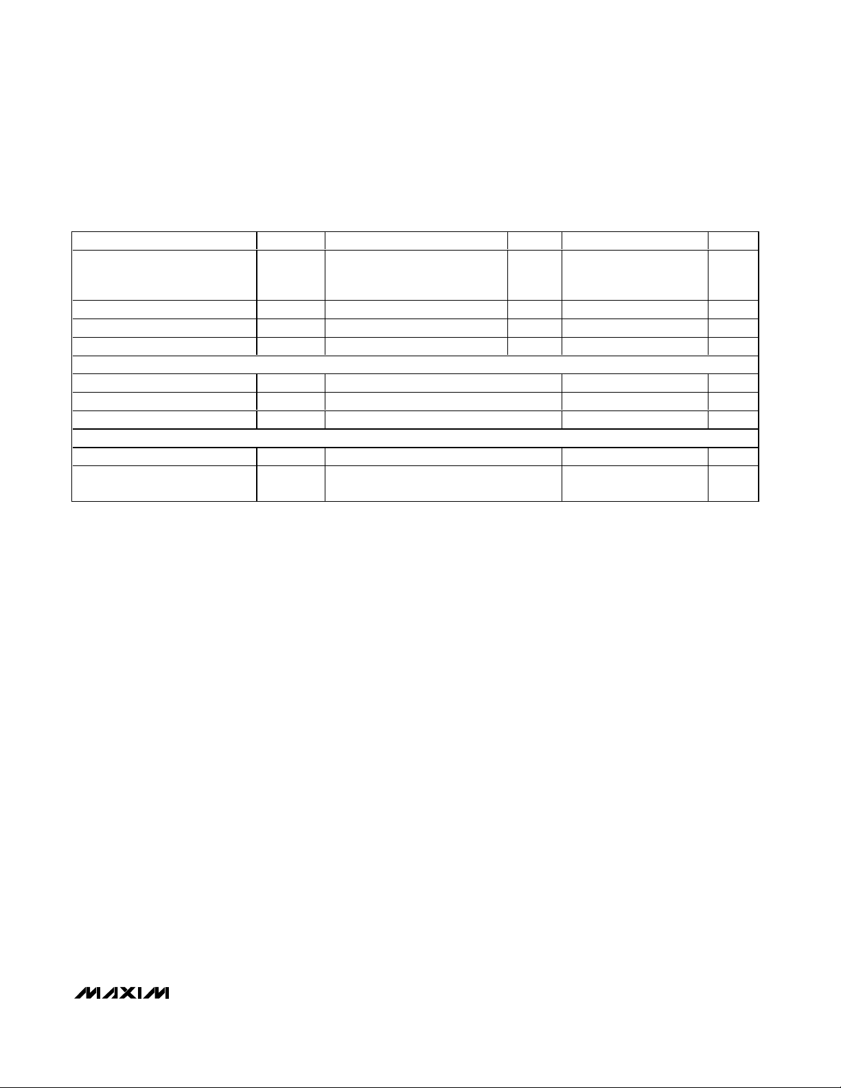
PART
TEMP
RANGE
TOP
MARK
MAX4731EUA
8 µMAX —
MAX4731ETA
ALG
MAX4731EBL-
9 UCSP-9
ABV
MAX4732EUA
8 µMAX —
MAX4732ETA
ALH
MAX4732EBL-
9 UCSP-9 ABT
MAX4733EUA
8 µMAX —
MAX4733ETA
ALI
MAX4733EBL-
9 UCSP-9
ABS
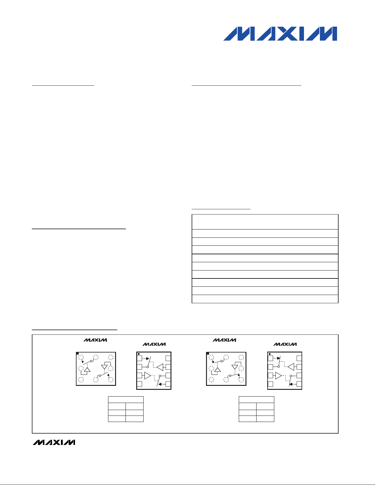
NO2
V+
GND
IN2
IN1
NO1
COM1
COM2
TOP VIEW
(BUMPS
ON BOTTOM)
UCSP
MAX4731
A1
B1
C1
C2
C3
B3
A3A2
MAX4732
NC2V+
GND
IN2
IN1
NC1
COM1
COM2
UCSP
A1
B1
C1
C2
C3
B3
A3A2
IN_
0
1
NO_
MAX4731
OFF
ON
SWITCHES SHOWN
FOR LOGIC "0" INPUT
IN_
0
1
NC_
MAX4732
ON
OFF
SWITCHES SHOWN
FOR LOGIC "0" INPUT
COM1
GND
NO1
TDFN
MAX4731
COM2
NO2
IN1
1
2
IN2
3
4
8
7
6
5
COM1
GND
NC1
TDFN
MAX4732
IN1
COM2
V+
1
2
IN2
3
4
8
7
6
5
TOP VIEW
(BUMPS
ON BOTTOM)
V+
NC2
Pin Configurations/Functional Diagrams/Truth Tables
UCSP is a trademark of Maxim Integrated Products, Inc.
µMAX is a registered trademark of Maxim Integrated Products, Inc.
Pin Configurations/Functional
Diagrams/Truth Tables
continued at end of data sheet.
*Future product—contact factory for availability.
**EP = Exposed pad.
PIN/BUMPPACKAGE
-40°C to +85°C
-40°C to +85°C 8 TDFN-EP**
-40°C to +85°C
-40°C to +85°C
-40°C to +85°C 8 TDFN-EP**
-40°C to +85°C
-40°C to +85°C
-40°C to +85°C 8 TDFN-EP**
-40°C to +85°C
Page 2
MAX4731/MAX4732/MAX4733
50
Ω,
Dual SPST Analog Switches in UCSP
2 _______________________________________________________________________________________
ABSOLUTE MAXIMUM RATINGS
ELECTRICAL CHARACTERISTICS—Single +3V Supply
(V+ = +3V ±10%, VIH= +2.0V, VIL= +0.8V, TA= T
MIN
to T
MAX
, unless otherwise noted. Typical values are at V+ = +3V, TA= +25°C.)
(Notes 3, 4)
Stresses beyond those listed under “Absolute Maximum Ratings” may cause permanent damage to the device. These are stress ratings only, and functional
operation of the device at these or any other conditions beyond those indicated in the operational sections of the specifications is not implied. Exposure to
absolute maximum rating conditions for extended periods may affect device reliability.
(All voltages referenced to GND.)
V+ ...........................................................................-0.3V to +12V
IN_, COM_, NO_, NC_ (Note 1)....................-0.3V to (V+ + 0.3V)
Continuous Current (any pin) ...........................................±10mA
Peak Current (any pin, pulsed at 1ms, 10% duty cycle) ...±20mA
Continuous Power Dissipation (T
A
= +70°C)
8-Pin µMAX (derate 4.5mW/°C above +70°C) .............362mW
8-Pin TDFN (derate 24.4mW/°C above +70°C) .........1951mW
9-Bump UCSP (derate 4.7mW/°C above +70°C).........379mW
Operating Temperature Range ...........................-40°C to +85°C
Storage Temperature Range .............................-65°C to +150°C
Maximum Junction Temperature .....................................+150°C
Lead Temperature (soldering, 10s) .................................+300°C
Bump Temperature (soldering, Note 2)
Infrared (15s) ...............................................................+220°C
Vapor Phase (60s) .......................................................+215°C
Note 1: Signals on IN_, NO_, NC_, or COM_ exceeding V+ or GND are clamped by internal diodes. Limit forward-diode current to
maximum current rating.
Note 2: This device is constructed using a unique set of packaging techniques that impose a limit on the thermal profile the device
can be exposed to during board level solder attach and rework. This limit permits only the use of the solder profiles recommended in the industry-standard specification, JEDEC 020A, paragraph 7.6, Table 3 for IR/VPR and Convection reflow. Preheating is required. Hand or wave soldering is not allowed.
PARAMETER
CONDITIONS T
A
UNITS
ANALOG SWITCH
Analog Signal Range
V
COM_
,
0V+V
19 50
On-Resistance R
ON
V+ = +2.7V,
I
COM_
= 5mA;
V
NO_
or V
NC_
= +1.5V
T
MIN
to
60
Ω
0.8 3.5
On-Resistance Matching
Between Channels (Notes 5, 6)
∆R
ON
V+ = +2.7V,
I
COM_
= 5mA;
V
NO_
or V
NC_
= +1.5V
T
MIN
to
4.5
Ω
2.3 9
On-Resistance Flatness
(Note 7)
)
V+ = +2.7V,
I
COM_
= 5mA;
T
MIN
to
11
Ω
NO_ or NC_ Off-Leakage Current
(Note 8)
)
)
V+ = +3.6V,
V
COM_
= +0.3V, +3V;
V
NO_
or V
NC_
= +3V, +0.3V
T
MIN
to
-2 +2
nA
COM_ Off-Leakage Current
(Note 8)
)
V+ = +3.6V,
V
COM_
= +0.3V, +3V;
V
NO_
or V
NC_
= +3V, +0.3V
T
MIN
to
-2 +2
nA
COM_ On-Leakage Current
(Note 8)
)
V+ = +3.6V,
V
COM_
= +0.3V, +3.0V;
V
NO_
or V
NC_
= +0.3V, +3V, or
floating
T
MIN
to
-4 +4
nA
SYMBOL
MIN TYP MAX
V
, V
NO_
NC_
R
FLAT(ON
I
I
I
COM_(OFF
I
COM_(ON
NO_(OFF
NC_(OFF
V
or V
NO_
NC_
= +1V, +1.5V, +2V
+25°C
T
MAX
+25°C
T
MAX
+25°C
T
MAX
+25°C -0.1 +0.1
T
MAX
+25°C -0.1 +0.1
T
MAX
+25°C -0.2 +0.2
T
MAX
Page 3
MAX4731/MAX4732/MAX4733
50
Ω,
Dual SPST Analog Switches in UCSP
_______________________________________________________________________________________ 3
ELECTRICAL CHARACTERISTICS—Single +3V Supply (continued)
(V+ = +3V ±10%, VIH= +2.0V, VIL= +0.8V, TA= T
MIN
to T
MAX
, unless otherwise noted. Typical values are at V+ = +3V, TA= +25°C.)
(Notes 3, 4)
PARAMETER
CONDITIONS T
A
UNITS
DYNAMIC CHARACTERISTICS
70 150
Turn-On Time t
ON
V
NO_
or V
NC_
= +1.5V,
R
L
= 300Ω,
C
L
= 35pF, Figure 2
T
MIN
to
170
ns
30 60
Turn-Off Time t
OFF
V
NO_
or V
NC_
= +1.5V,
R
L
= 300Ω, CL = 35pF,
Figure 2
T
MIN
to
70
ns
40
Break-Before-Make
(MAX4733 Only, Note 8)
t
BBM
V
NO_
or V
NC_
= +1.5V,
R
L
= 300Ω, CL = 35pF,
Figure 3
T
MIN
to
1
ns
Charge Injection Q
V
GEN
= 0V, R
GEN
= 0, CL = 1.0nF,
Figure 4
7.5 pC
On-Channel -3dB Bandwidth BW Signal = 0dBm, 50Ω in and out
MHz
Off-Isolation (Note 9) V
ISO
f = 1MHz, V
COM_
= 1V
RMS
,
R
L
= 50Ω, CL = 5pF,
Figure 5
-72 dB
Crosstalk (Note 10) V
CT
f = 1MHz, V
COM_
= 1V
RMS
,
R
L
= 50Ω, CL = 5pF,
Figure 6
dB
NO_ or NC_ Off-Capacitance C
OFF
f = 1MHz, Figure 7
20 pF
COM_ Off-Capacitance
)
f = 1MHz, Figure 7
20 pF
COM_ On-Capacitance
)
f = 1MHz, Figure 7
40 pF
LOGIC INPUT
Input Logic High V
IH
1.4 V
Input Logic Low V
IL
0.8 V
Input Leakage Current I
IN
V
IN_
= 0V or V+ -1
+1 µA
SUPPLY
Power-Supply Range V+ 2.0 11 V
Positive Supply Current I+
V+ = +5.5V, V
IN_
= 0V or V+,
all switches on or off
1µA
SYMBOL
C
COM_(OFF
C
COM_(ON
MIN TYP MAX
+25°C
T
MAX
+25°C
T
MAX
+25°C
T
MAX
+25°C
+25°C 300
+25°C
+25°C -108
+25°C
+25°C
+25°C
+0.005
0.0001
Page 4
MAX4731/MAX4732/MAX4733
50
Ω,
Dual SPST Analog Switches in UCSP
4 _______________________________________________________________________________________
ELECTRICAL CHARACTERISTICS—Single +5V Supply
(V+ = +5V ±10%, VIH= +2.0V, VIL= +0.8V, TA= T
MIN
to T
MAX
, unless otherwise noted. Typical values are at V+ = +5V, TA= +25°C.)
(Notes 3, 4)
PARAMETER
CONDITIONS T
A
UNITS
ANALOG SWITCH
Analog Signal Range
V
COM_
,
0V+V
8.5 25
On-Resistance R
ON
V+ = +4.5V,
I
COM_
= 5mA,
V
NO_
or V
NC_
= +3.5V
T
MIN
to
30
Ω
0.2 3
On-Resistance Matching
Between Channels (Notes 5, 6)
∆R
ON
V+ = +4.5V,
I
COM_
= 5mA,
V
NO_
or V
NC_
= +3.5V
T
MIN
to
4
Ω
25
On-Resistance Flatness
(Note 7)
)
V+ = +4.5V,
I
COM_
= 5mA,
V
NO_
or V
NC_
= +1V, +2V, +3V
T
MIN
to
7
Ω
NO_ or NC_ Off-Leakage Current
(Note 8)
)
)
V+ = +5.5V,
V
COM_
= +1V, +4.5V;
V
NO_
or V
NC_
= +4.5V, +1V
T
MIN
to
-2 +2
nA
COM_ Off-Leakage Current
(Note 8)
)
V+ = +5.5V,
V
COM_
= +1V, +4.5V;
V
NO_
or V
NC_
= +4.5V, +1V
T
MIN
to
-2 +2
nA
COM_ On-Leakage Current
(Note 8)
)
V+ = +5.5V,
V
COM_
= +1V, +4.5V;
V
NO_
or V
NC_
= +1V, +4.5V, or
floating
T
MIN
to
-4 +4
nA
DYNAMIC CHARACTERISTICS
47 85
Turn-On Time t
ON
V
NO_
or V
NC_
= +3.0V,
R
L
= 300Ω, CL = 35pF,
Figure 2
T
MIN
to
95
ns
23 45
Turn-Off Time t
OFF
V
NO_
or V
NC_
= +3.0V,
R
L
= 300Ω, CL = 35pF,
Figure 2
T
MIN
to
55
ns
25
Break-Before-Make
(MAX4733 Only, Note 8)
t
BBM
V
NO_
or V
NC_
= +3.0V,
R
L
= 300Ω, CL = 35pF,
Figure 3
T
MIN
to
1
ns
Charge Injection Q
V
GEN
= 0V, R
GEN
= 0,
C
L
= 1.0nF, Figure 4
7.5 pC
On-Channel Bandwidth BW
Signal = 0dBm,
50Ω in and out
MHz
Off-Isolation (Note 9) V
ISO
f = 1MHz, V
COM_
= 1V
RMS
,
R
L
= 50Ω, CL = 5pF,
Figure 5
-72 dB
SYMBOL
V
, V
NO_
R
FLAT(ON
I
NO_(OFF
I
NC_(OFF
I
COM_(OFF
I
COM_(ON
NC_
MIN TYP MAX
+25°C
T
MAX
+25°C
T
MAX
+25°C
T
MAX
+25°C -0.1 +0.1
T
MAX
+25°C -0.1 +0.1
T
MAX
+25°C -0.2 +0.2
T
MAX
+25°C
T
MAX
+25°C
T
MAX
+25°C
T
MAX
+25°C
+25°C 300
+25°C
Page 5
MAX4731/MAX4732/MAX4733
50
Ω,
Dual SPST Analog Switches in UCSP
_______________________________________________________________________________________ 5
Note 3: The algebraic convention, where the most negative value is a minimum and the most positive value a maximum, is used in
this data sheet.
Note 4: UCSP and TDFN parts are 100% tested at +25°C only, and guaranteed by design over temperature. µMAX parts are
100% tested at +85°C and +25°C and guaranteed by design over temperature.
Note 5: ∆R
ON
= R
ON(MAX)
- R
ON(MIN)
.
Note 6: UCSP on-resistance matching between channels and on-resistance flatness guaranteed by design.
Note 7: Flatness is defined as the difference between the maximum and minimum value of on-resistance as measured over the
specified analog signal range.
Note 8: Guaranteed by design.
Note 9: Off-Isolation = 20 log
10(VNO_/VCOM_
), V
NO_
= output, V
COM_
= input to off switch.
Note 10: Between any two switches.
ELECTRICAL CHARACTERISTICS—Single +5V Supply
(V+ = +5V ±10%, VIH= +2.0V, VIL= +0.8V, TA= T
MIN
to T
MAX
, unless otherwise noted. Typical values are at V+ = +5V, TA= +25°C.)
(Notes 3, 4)
PARAMETER
SYMBOL
CONDITIONS T
A
MIN
TYP
MAX
UNITS
Crosstalk (Note 10) V
CT
f = 1MHz, V
COM_
= 1V
RMS
,
R
L
= 50Ω, CL = 5pF,
Figure 6
dB
NO_ or NC_ Off-Capacitance C
OFF
f = 1MHz, Figure 7
20 pF
COM_ Off-Capacitance
)
f = 1MHz, Figure 7
20 pF
COM_ On-Capacitance
)
f = 1MHz, Figure 7
40 pF
LOGIC INPUT
Input Logic High V
IH
2.0 V
Input Logic Low V
IL
0.8 V
Input Leakage Current I
IN
V
IN_
= 0V or V+ -1
+1 µA
SUPPLY
Power-Supply Range V+ 2.0 11 V
Positive Supply Current I+
V+ = +5.5V, V
IN_
= 0V or V+,
all switches on or off
1µA
C
COM_(OFF
C
COM_(ON
+25°C -108
+25°C
+25°C
+25°C
+0.005
0.0001
Page 6
MAX4731/MAX4732/MAX4733
50
Ω,
Dual SPST Analog Switches in UCSP
6 _______________________________________________________________________________________
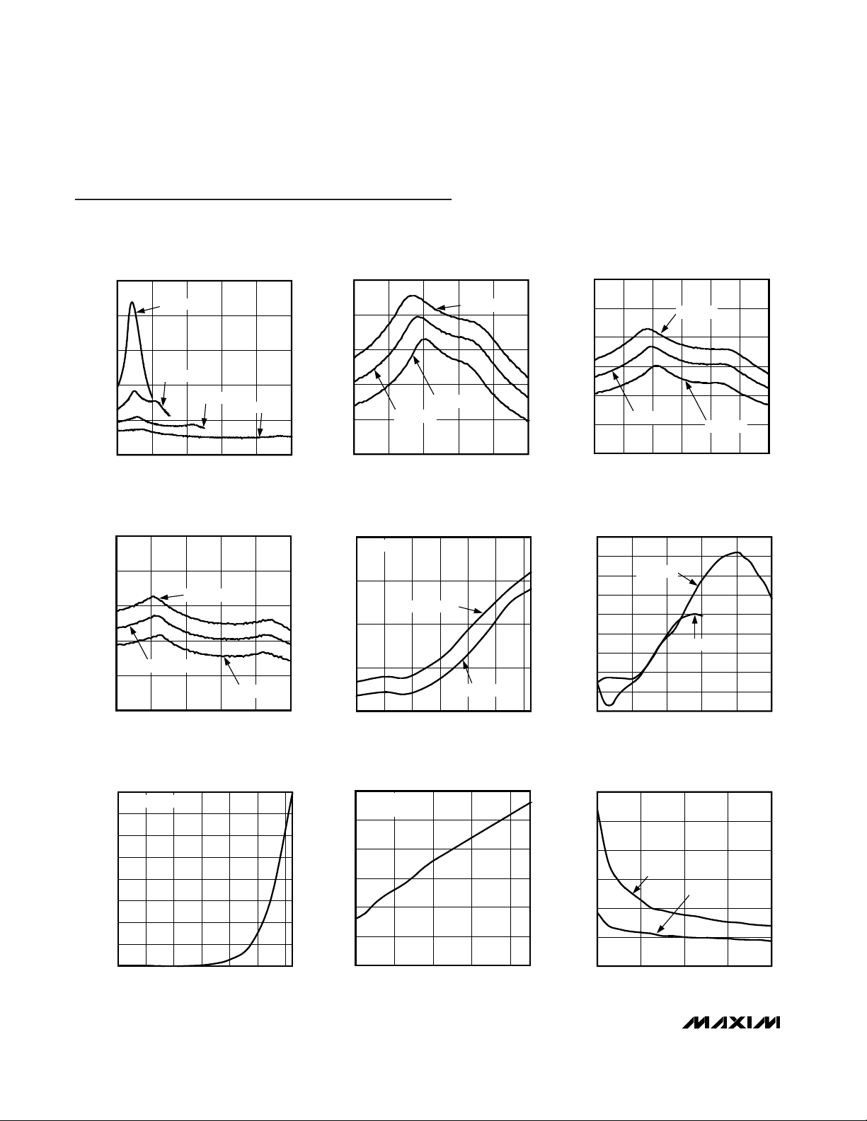
Typical Operating Characteristics
(TA = +25°C, unless otherwise noted.)
ON-RESISTANCE vs. V
COM
MAX4731-33 toc01
V
COM
(V)
R
ON
(Ω)
8642
10
20
30
40
50
0
010
V+ = +2.0V
V+ = +3.0V
V+ = +5.0V
V+ = +10.0V
ON-RESISTANCE
vs. V
COM
(V+ = +2.5V)
MAX4731-33 toc02
V
COM
(V)
R
ON
(Ω)
2.01.51.00.5
10
15
20
25
30
5
0 2.5
TA = +85°C
TA = -40°C
TA = +25°C
ON-RESISTANCE
vs. V
COM
(V+ = +3.0V)
MAX4731-33 toc03
V
COM
(V)
R
ON
(Ω)
2.01.51.00.5
10
15
20
25
30
0
5
03.02.5
TA = +85°C
TA = -40°C
TA = +25°C
ON-RESISTANCE
vs. V
COM
(V+ = +5.0V)
MAX4731-33 toc04
V
COM
(V)
R
ON
(Ω)
4321
4
8
12
16
20
0
05
TA = +85°C
TA = -40°C
TA = +25°C
ON/OFF-LEAKAGE CURRENT
vs. TEMPERATURE
MAXZ4731-33 toc05
TEMPERATURE (°C)
ON/OFF-LEAKAGE CURRENT (pA)
6040200-20
1
10
100
1000
0
-40 80
V+ = +5V
ON-LEAKAGE
OFF-LEAKAGE
CHARGE INJECTION vs. V
COM
MAX4731-33 toc06
V
COM
(V)
CHARGE INJECTION (pC)
4321
5
10
15
20
25
30
35
40
45
0
05
V+ = +5.0V
V+ = +3.0V
SUPPLY CURRENT vs. TEMPERATURE
MAX4731-33 toc07
TEMPERATURE (°C)
SUPPLY CURRENT (nA)
8060-20 0 20 40
0.5
1.0
1.5
2.0
2.5
3.0
3.5
4.0
0
-40
V+ = +5V, +3V
LOGIC THRESHOLD VOLTAGE
vs. SUPPLY VOLTAGE
MAX4731-33 toc08
V+ (V)
LOGIC THRESHOLD VOLTAGE (V)
10864
0.5
1.0
1.5
2.0
2.5
3.0
0
2
VIN RISING OR
FALLING
TURN-ON/OFF TIME
vs. SUPPLY VOLTAGE
MAX4731-33 toc09
V+ (V)
t
ON/OFF
(ns)
864
20
40
60
80
100
120
0
210
t
ON
t
OFF
Page 7

Applications Information
Operating Considerations for
High-Voltage Supply
The MAX4731/MAX4732/MAX4733 operate to +11V
with some precautions. The absolute maximum rating
for V+ is +12V (referenced to GND). When operating
near this region, bypass V+ with a minimum 0.1µF
capacitor to ground as close to the IC as possible.
Logic Levels
The MAX4731/MAX4732/MAX4733 are TTL compatible
when powered from a single +5V supply. When powered from other supply voltages, the logic inputs should
be driven rail-to-rail. For example, with a +11V supply,
IN1 and IN2 should be driven low to 0V and high to
11V. With a +3.3V supply, IN1 and IN2 should be driven low to 0V and high to 3.3V. Driving IN1 and IN2 railto-rail minimizes power consumption.
MAX4731/MAX4732/MAX4733
50
Ω,
Dual SPST Analog Switches in UCSP
_______________________________________________________________________________________ 7
Pin Description
Typical Operating Characteristics (continued)
(TA = +25°C, unless otherwise noted.)
TURN-ON/OFF TIME
vs. TEMPERATURE
MAX4731-33 toc10
TEMPERATURE (°C)
t
ON/OFF
(ns)
6040-20 0 20
10
20
30
40
50
60
70
80
0
-40 80
tON,
V+ = +3.0V
tON,
V+ = +5.0V
t
OFF
,
V+ = +3.0V
t
OFF
,
V+ = +5.0V
FREQUENCY RESPONSE
MAX4731-33 toc11
FREQUENCY (Hz)
LOSS (dB)
100M10M1M100k
-100
-80
-60
-40
-20
0
-120
10k 1G
ON-LOSS
V+ = +3V
OFF-ISOLATION
CROSSTALK
TOTAL HARMONIC DISTORTION
vs. FREQUENCY
MAX4731-33 toc12
FREQUENCY (Hz)
THD (%)
10k1k100
0.001
0.01
0.1
1
0.0001
10 100k
V
COM
= 2V
P-P
BW = 30kHz
RL = 1k
Ω
V+ = +3.0V
RL = 1k
Ω
V+ = +5.0V
RL = 100k
Ω
V+ = +3.0V
RL = 100k
Ω
V+ = +5.0V
PIN
MAX4731 MAX4732 MAX4733
UCSP
µMAX/
TDFN
µMAX/
TDFN
UCSP
TDFN
NAME FUNCTION
A1 1 —— A1 1 NO1 Analog-Switch Normally Open Terminal
A2 2 A2 2 A2 2 COM1 Analog-Switch Common Terminal
A3 4 A3 4 A3 4 GND Ground. Connect to digital ground.
B1 7 B1 7 B1 7 IN1 Logic-Control Digital Input
B3 3 B3 3 B3 3 IN2 Logic-Control Digital Input
C1 8 C1 8 C1 8 V+ Positive Supply Voltage Input
C2 6 C2 6 C2 6 COM2 Analog-Switch Common Terminal
C3 5 —— ——NO2 Analog-Switch Normally Open Terminal
——A1 1 ——NC1 Analog-Switch Normally Closed Terminal
——C3 5 C3 5 NC2 Analog-Switch Normally Closed Terminal
—
EP (TDFN
y)
—
EP (TDFN
y)
—
EP (TDFN
y)
EP Exposed Pad. Connect to V+.
UCSP
µMAX/
onl
onl
onl
Page 8

MAX4731/MAX4732/MAX4733
Analog Signal Levels
Analog signals that range over the entire supply voltage
(GND to V+) pass with very little change in RON(see
Typical Operating Characteristics). The bidirectional
switches allow NO_, NC_, and COM_ connections to be
used as either inputs or outputs.
Power-Supply Sequencing and
Overvoltage Protection
CAUTION: Do not exceed the absolute maximum
ratings. Stresses beyond the listed ratings can
cause permanent damage to the devices.
Proper power-supply sequencing is recommended for
all CMOS devices. Always apply V+ before applying
analog signals, especially if the analog signal is not
current limited. If this sequencing is not possible, and if
the analog inputs are not current limited to < 20mA,
add a small-signal diode, D1, as shown in Figure 1. If
the analog signal can dip below GND, add D2. Adding
protection diodes reduces the analog signal range to a
diode drop (about 0.7V) below V+ (for D1), and to a
diode drop above ground (for D2). Leakage is unaffected by adding the diodes. On-resistance increases
slightly at low supply voltages. Maximum supply voltage (V+) must not exceed +11V.
Adding protection diodes causes the logic thresholds to
be shifted relative to the power-supply rails. The most
significant shift occurs when using low supply voltages
(+5V or less). With a +5V supply, TTL compatibility is not
guaranteed when protection diodes are added. Driving
IN1 and IN2 all the way to the supply rails (i.e., to a
diode drop higher than the V+ pin, or to a diode drop
lower than the GND pin) is always acceptable.
Protection diodes D1 and D2 also protect against some
overvoltage situations. Using the circuit in Figure 1, no
damage results if the supply voltage is below the
absolute maximum rating (+12V) and if a fault voltage
up to the absolute maximum rating (V+ + 0.3V) is
applied to an analog signal terminal.
UCSP Applications Information
For the latest application details on USCP construction,
dimensions, tape carrier information, printed circuit
board techniques, bump-pad layout, and recommended reflow temperature profile as well as the latest information on reliability testing results, go to the Maxim
web site at www.maxim-ic.com/ucsp to find the
Application Note: UCSP—A Wafer-Level Chip-Scale
Package.
50
Ω,
Dual SPST Analog Switches in UCSP
8 _______________________________________________________________________________________
MAX4731
MAX4732
MAX4733
NO_ COM_
GND
V+
*INTERNAL PROTECTION DIODES.
D2
D1
EXTERNAL BLOCKING DIODE
EXTERNAL BLOCKING DIODE
GND
V+
*
*
*
*
Figure 1. Overvoltage Protection Using External Blocking Diodes
Test Circuits/Timing Diagrams
Page 9

MAX4731/MAX4732/MAX4733
50
Ω,
Dual SPST Analog Switches in UCSP
_______________________________________________________________________________________ 9
Test Circuits/Timing Diagrams (continued)
50%
V
IL
LOGIC
INPUT
R
L
300
Ω
IN_
C
L
INCLUDES FIXTURE AND STRAY CAPACITANCE.
(
R
L
)
V
N_
V
IH
t
OFF
0V
NO_
OR NC_
0.9 x V
OUT
0.9 x V
OUT
t
ON
V
OUT
SWITCH
OUTPUT
LOGIC
INPUT
LOGIC INPUT WAVEFORMS INVERTED FOR SWITCHES
THAT HAVE THE OPPOSITE LOGIC SENSE.
V+
COM_
C
L
35pF
V+
V
OUT
MAX4731
MAX4732
MAX4733
GND
R
L
+ R
ON
tr < 5ns
t
f
< 5ns
V
OUT
= V
N_
Figure 2. Switching Time
50%
0.9 x V
0UT1
V+
0V
0V
LOGIC
INPUT
SWITCH
OUTPUT 2
(V
OUT2
)
0V
0.9 x V
OUT2
t
BBM
t
BBM
LOGIC
INPUT
R
L2
300
Ω
GND
C
L
INCLUDES FIXTURE AND STRAY CAPACITANCE.
NC2
IN2
IN1
NO1
V
OUT2
V+
V+
C
L2
35pF
V
N_
R
L1
300
Ω
V
OUT1
C
L1
35pF
COM1
COM2
SWITCH
OUTPUT 1
(V
OUT1
)
MAX4733
tr < 5ns
t
f
< 5ns
Figure 3. Break-Before-Make Interval (MAX4733 only)
V
GEN
GND
COM
C
L
1nF
V
OUT
V+
V
OUT
IN
OFF
ON
OFF
∆V
OUT
Q = (∆V
OUT
)(CL)
NC_
OR NO_
IN DEPENDS ON SWITCH CONFIGURATION;
INPUT POLARITY DETERMINED BY SENSE OF SWITCH.
OFF
ON
OFF
IN
V
IL
TO V
IH
V+
R
GEN
IN_
MAX4731
MAX4732
MAX4733
Figure 4. Charge Injection
Page 10

MAX4731/MAX4732/MAX4733
50
Ω,
Dual SPST Analog Switches in UCSP
10 ______________________________________________________________________________________
IN_
V
IL
OR V
IH
SIGNAL
GENERATOR 0dBm
V+
10nF
ANALYZER
NC_
OR NO_
R
L
GND
COM_
V+
MAX4731
MAX4732
MAX4733
V-
NOTE: DUAL SUPPLIES USED TO ACCOMODATE GROUND-REFERENCED INSTRUMENTS.
10nF
Figure 5. Off-Isolation/On-Channel Bandwidth
SIGNAL
GENERATOR 0dBm
V+
10nF
ANALYZER
NO2/NC2
R
L
COM1
0 OR 2.4V
IN1
NO1/NC1
50Ω
COM2
IN2
0 OR 2.4V
N.C.
V+
MAX4731
MAX4732
MAX4733
GND
V-
NOTE: DUAL SUPPLIES USED TO ACCOMODATE GROUND-REFERENCED INSTRUMENTS.
10nF
Figure 6. Crosstalk
CAPACITANCE
METER
NC_ OR
NO_
COM_
GND
IN_
V
IL
OR V
IH
10nF
V+
f = 1MHz
V+
MAX4731
MAX4732
MAX4733
Figure 7. Channel Off/On-Capacitance
Chip Information
TRANSITOR COUNT: 68
PROCESS: CMOS
Test Circuits/Timing Diagrams (continued)
Page 11

MAX4731/MAX4732/MAX4733
50
Ω,
Dual SPST Analog Switches in UCSP
______________________________________________________________________________________ 11
TOP VIEW
µMAX
8
7
6
5
1
2
3
4
V+
IN1
COM2
NO2
GND
IN2
COM1
NO1
MAX4731 MAX4733
µMAX
8
7
6
5
1
2
3
4
V+
IN1
COM2
NC2
GND
IN2
COM1
NO1
µMAX
8
7
6
5
1
2
3
4
V+
IN1
COM2
NC2
GND
IN2
COM1
NC1
MAX4732
MAX4733
NC2V+
GND
IN2
IN1
NO1
COM1
COM2
A1
B1
C1
C2
C3
B3
A3A2
IN_
0
1
NO1
MAX4733
ON
OFF
SWITCHES SHOWN FOR LOGIC "0" INPUT
NC2
OFF
ON
COM1
GND
NO1
TDFN
MAX4733
COM2
NC2
IN1
1
2
IN2
3
4
8
7
6
5
UCSP
TOP VIEW
(BUMPS
ON BOTTOM)
V+
EP
EP = EXPOSED PAD
Pin Configurations/Functional Diagrams/Truth Tables (continued)
Page 12

MAX4731/MAX4732/MAX4733
50
Ω,
Dual SPST Analog Switches in UCSP
12 ______________________________________________________________________________________
Package Information
(The package drawing(s) in this data sheet may not reflect the most current specifications. For the latest package outline information
go to www.maxim-ic.com/packages
.)
9LUCSP, 3x3.EPS
PACKAGE OUTLINE, 3x3 UCSP
21-0093
1
1
K
Page 13

MAX4731/MAX4732/MAX4733
50
Ω,
Dual SPST Analog Switches in UCSP
______________________________________________________________________________________ 13
6, 8, &10L, DFN THIN.EPS
H
1
2
21-0137
PACKAGE OUTLINE, 6,8,10 & 14L,
TDFN, EXPOSED PAD, 3x3x0.80 mm
COMMON DIMENSIONS
SYMBOL
MIN. MAX.
A 0.70 0.80
D 2.90 3.10
E 2.90 3.10
A1
0.00 0.05
L 0.20 0.40
PKG. CODE N D2 E2 e JEDEC SPEC b [(N/2)-1] x e
PACKAGE VARIATIONS
0.25 MIN.k
A2 0.20 REF.
2.30–0.101.50–0.106T633-1 0.95 BSC MO229 / WEEA 1.90 REF0.40–0.05
1.95 REF0.30–0.050.65 BSC2.30–0.108T833-1
2.00 REF0.25–0.050.50 BSC2.30–0.1010T1033-1
2.40 REF0.20–0.05- - - - 0.40 BSC1.70–0.10 2.30–0.1014T1433-1
1.50–0.10
1.50–0.10
MO229 / WEEC
MO229 / WEED-3
0.40 BSC - - - - 0.20–0.05 2.40 REFT1433-2 14 2.30–0.101.70–0.10
T633-2 6 1.50–0.10 2.30–0.10
0.95 BSC MO229 / WEEA
0.40–0.05 1.90 REF
T833-2 8 1.50–0.10 2.30–0.10 0.65 BSC MO229 / WEEC 0.30–0.05 1.95 REF
T833-3 8 1.50–0.10 2.30–0.10 0.65 BSC MO229 / WEEC 0.30–0.05 1.95 REF
-DRAWING NOT TO SCALE-
H
2
2
21-0137
PACKAGE OUTLINE, 6,8,10 & 14L,
TDFN, EXPOSED PAD, 3x3x0.80 mm
2.30–0.10
MO229 / WEED-3
2.00 REF0.25–0.05
0.50 BSC
1.50–0.1010T1033-2
Package Information (continued)
(The package drawing(s) in this data sheet may not reflect the most current specifications. For the latest package outline information
go to www.maxim-ic.com/packages
.)
Page 14

Package Information (continued)
(The package drawing(s) in this data sheet may not reflect the most current specifications. For the latest package outline information
go to www.maxim-ic.com/packages
.)
MAX4731/MAX4732/MAX4733
50
Ω,
Dual SPST Analog Switches in UCSP
Maxim cannot assume responsibility for use of any circuitry other than circuitry entirely embodied in a Maxim product. No circuit patent licenses are
implied. Maxim reserves the right to change the circuitry and specifications without notice at any time.
14 ____________________Maxim Integrated Products, 120 San Gabriel Drive, Sunnyvale, CA 94086 408-737-7600
© 2006 Maxim Integrated Products is a registered trademark of Maxim Integrated Products, Inc.
8LUMAXD.EPS
PACKAGE OUTLINE, 8L uMAX/uSOP
1
1
21-0036
J
REV.DOCUMENT CONTROL NO.APPROVAL
PROPRIETARY INFORMATION
TITLE:
MAX
0.043
0.006
0.014
0.120
0.120
0.198
0.026
0.007
0.037
0.0207 BSC
0.0256 BSC
A2
A1
c
e
b
A
L
FRONT VIEW
SIDE VIEW
E H
0.6–0.1
0.6–0.1
fl0.50–0.1
1
TOP VIEW
D
8
A2
0.030
BOTTOM VIEW
1
6¡
S
b
L
H
E
D
e
c
0¡
0.010
0.116
0.116
0.188
0.016
0.005
8
4X S
INCHES
-
A1
A
MIN
0.002
0.950.75
0.5250 BSC
0.25 0.36
2.95 3.05
2.95 3.05
4.78
0.41
0.65 BSC
5.03
0.66
6¡0¡
0.13 0.18
MAX
MIN
MILLIMETERS
- 1.10
0.05 0.15
α
α
DIM
Revision History
Pages changed at Rev 2: 1, 2, 7, 8, 11, 14
 Loading...