

Page 1
General Description
The MAX4721/MAX4722/MAX4723 low-voltage, low onresistance (RON), dual single-pole/single throw (SPST)
analog switches operate from a single +1.8V to +5.5V
supply. These devices are designed for USB 1.1 and
audio switching applications.
The MAX4721/MAX4722/MAX4723 feature 4.5Ω R
ON
(max) with 1.2Ω flatness and 0.3Ω matching between
channels. These new switches feature guaranteed
operation from +1.8V to +5.5V and are fully specified at
3V and 5V. These switches offer break-before-make
switching (1ns) with tON<80ns and t
OFF
<40ns at
+2.7V. The digital logic inputs are +1.8V logic compatible with a +2.7V to +3.6V supply.
These switches are packaged in a chip-scale package
(UCSP™), significantly reducing the required PC board
area. The chip occupies only a 1.52mm ✕ 1.52mm area
and has a 3 ✕ 3 bump array with a bump pitch of
0.5mm. These switches are also available in an 8-pin
µMAX package.
Applications
Battery-Operated Equipment
Audio/Video-Signal Routing
Low-Voltage Data-Acquisition Systems
Sample-and-Hold Circuits
Communications Circuits
Features
♦ USB 1.1 Signal Switching
♦ <2ns Differential Skew
♦ -3dB Bandwidth: >300MHz
♦ Low 15pF On-Channel Capacitance
♦ Low RON(max) Switches
4.5Ω (max) (+3V Supply)
3Ω (max) (+5V Supply)
♦ 0.3Ω (max) R
ON
Match (+3V Supply)
♦ 1.2Ω (max) R
ON
Flatness (+3V Supply)
♦ <0.5nA Leakage Current at TA= +25°C
♦ High Off-Isolation: -55dB (10MHz)
♦ Low Crosstalk: -80dB (10MHz)
♦ Low Distortion: 0.03%
♦ +1.8V CMOS-Logic Compatible
♦ Single-Supply Operation from +1.8V to +5.5V
♦ Rail-to-Rail®Signal Handling
MAX4721/MAX4722/MAX4723
4.5
Ω
Dual SPST Analog Switches in UCSP
________________________________________________________________ Maxim Integrated Products 1
Ordering Information
19-2632; Rev 0; 10/02
For pricing, delivery, and ordering information, please contact Maxim/Dallas Direct! at
1-888-629-4642, or visit Maxim’s website at www.maxim-ic.com.
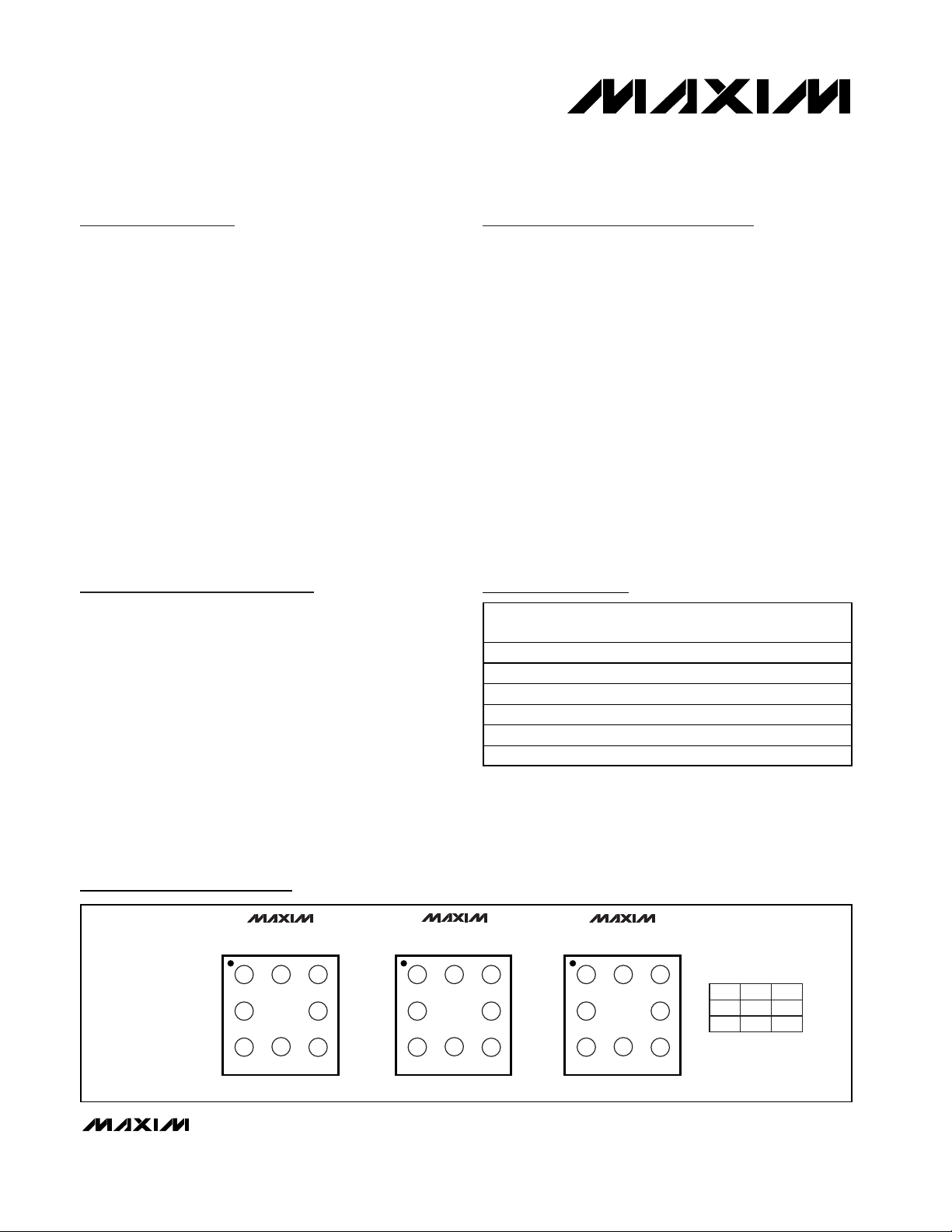
Pin Configurations/Functional Diagrams/Truth Tables
Rail-to-Rail is a registered trademark of Nippon Motorola, Ltd.
UCSP is a trademark of Maxim Integrated Products, Inc.
Note: UCSP package requires special solder temperature profile described in the Absolute Maximum Ratings section.
*UCSP reliability is integrally linked to the user’s assembly methods, circuit board material, and environment. See the UCSP reliability notice in the UCSP Reliability section of this data sheet for
more information.
PART TEMP RANGE
MAX4721EUA -40°C to +85°C 8 µMAX —
MAX4721EBL-T* -40°C to +85°C 9 UCSP-9 ABP
MAX4722EUA -40°C to +85°C 8 µMAX —
MAX4722EBL-T* -40°C to +85°C 9 UCSP-9 ABQ
MAX4723EUA -40°C to +85°C 8 µMAX —
MAX4723EBL-T* -40°C to +85°C 9 UCSP-9 ABR
PIN/BUMPPACKAGE
TOP
MARK
MAX4721
TOP VIEW
(BUMP SIDE DOWN)
123
A
IN2
GNDV+NO2
B
COM1
C
NO1
COM2
IN1
UCSP
A
B
C
MAX4722
123
IN2
GNDV+NC2
COM1
NC1
COM2
IN1
UCSP
MAX4723
123
A
IN2
GNDV+NC2
B
COM1
C
NO1
UCSP
COM2
IN1
IN_
LOW
HIGH
NO_
OFF
ON
NC_
ON
OFF
Page 2
MAX4721/MAX4722/MAX4723
4.5
Ω
Dual SPST Analog Switches in UCSP
2 _______________________________________________________________________________________
ABSOLUTE MAXIMUM RATINGS
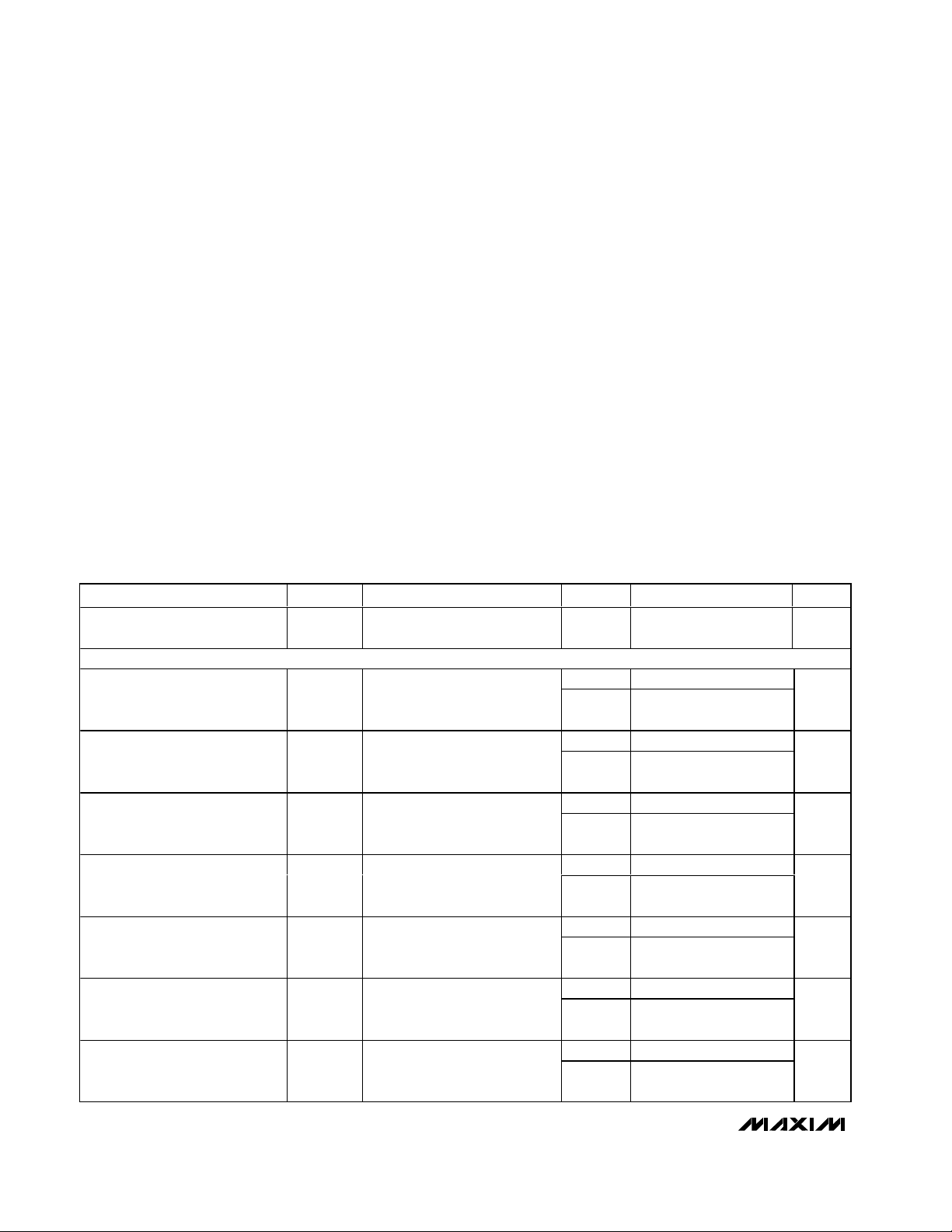
ELECTRICAL CHARACTERISTICS—Single +3V Supply
(V+ = +2.7V to +3.6V, VIH= +1.4V, VIL= +0.5V, TA= T
MIN
to T
MAX
, unless otherwise noted. Typical values are at V+ = +3.0V,
T
A
= +25°C, unless otherwise noted.) (Notes 3, 4)
Stresses beyond those listed under “Absolute Maximum Ratings” may cause permanent damage to the device. These are stress ratings only, and functional
operation of the device at these or any other conditions beyond those indicated in the operational sections of the specifications is not implied. Exposure to
absolute maximum rating conditions for extended periods may affect device reliability.
(All Voltages Referenced to GND, Unless Otherwise Noted.)
V+, IN_...................................................................-0.3V to +6.0V
COM_, NO_, NC_ (Note 1) ...........................-0.3V to (V+ + 0.3V)
Continuous Current COM_, NO_, NC_ ...........................±100mA
Peak Current COM_, NO_, NC_
(pulsed at 1ms, 10% duty cycle)................................±200mA
Continuous Power Dissipation (T
A
= +70°C)
8-Pin µMAX (derate 4.5mW/°C above +70°C) .............362mW
9-Bump UCSP (derate 4.7mW/°C above +70°C).........379mW
ESD Method 3015.7 .............................................................>2kV
Operating Temperature Range ...........................-40°C to +85°C
Junction Temperature......................................................+150°C
Storage Temperature Range .............................-65°C to +150°C
Lead Temperature (soldering, 10s) .................................+300°C
Bump Temperature (soldering) (Note 2)
Infrared (15s) ...............................................................+220°C
Vapor Phase (60s) .......................................................+215°C
Note 1: Signals on COM_, NO_, or NC_ exceeding V+ or GND are clamped by internal diodes. Limit forward-diode current to maxi-
mum current rating.
Note 2: This device is constructed using a unique set of packaging techniques that impose a limit on the thermal profile the device
can be exposed to during board level solder attach and rework. This limit permits only the use of the solder profiles recommended in the industry standard specification, JEDEC 020A, paragraph 7.6, table 3 for IR/VPR and convection reflow.
Preheating is required. Hand or wave soldering is not allowed.
)
),
)
)
Analog Signal Range
PARAMETER SYMBOL CONDITIONS T
V
,
COM_
V
, V
NO_
NC_
ANALOG SWITCH
On-Resistance (Note 5) R
On-Resistance Match Between
Channels (Notes 5, 6)
On-Resistance Flatness (Note 7) R
NO_, NC_ Off-Leakage Current
(Note 8)
COM_ Off-Leakage Current
(Note 8)
COM_ On-Leakage Current
(Note 8)
Turn-On Time t
∆R
FLAT(ON
I
NO_(OFF
I
NC_(OFF
I
C OM _ (OF F) ,
I
C OM _ (OF F)
I
COM_(ON
ON
ON
ON
V+ = 2.7V, I
or V
V
NO_
V+ = 2.7V, I
or V
V
NO_
V+ = 2.7V, I
V
or V
NO_
V+ = 3.6V, V
or V
V
NO_
V+ = 3.6V, V
V
or V
NO_
V+ = 3.6V, V
V
or V
NO_
floating
V
, V
NO_
= 300Ω, CL = 35pF, Figure 1
R
L
NC_
NC_
= 10mA;
COM_
= 1.5V
NC_
= 10mA;
COM_
= 1.5V
NC_
= 10mA;
COM_
= 1.0V, 1.5V, 2.0V
NC_
= 0.3V, 3.3V;
COM_
= 3.3V, 0.3V
NC_
= 0.3V, 3.3V;
COM_
= 3.3V, 0.3V
= 0.3V, 3.3V;
COM_
= 0.3V, 3.3V, or
NC_
= 1.5V;
A
MIN TYP MAX UNITS
0V+V
+25°C 3.0 4.5
T
to
MIN
T
MAX
5
+25°C 0.1 0.3
T
to
MIN
T
MAX
0.4
+25°C 0.6 1.2
T
to
MIN
T
MAX
1.5
+25°C -0.5 +0.01 +0.5
T
to
MIN
T
MAX
-1.5 +1.5
+25°C -0.5 +0.01 +0.5
to
T
MIN
T
MAX
-1.5 +1.5
+25°C -1 +0.01 +1
to
T
MIN
T
MAX
-2 +2
+25°C4080
T
to
MIN
T
MAX
100
Ω
Ω
Ω
nA
nA
nA
ns
Page 3
MAX4721/MAX4722/MAX4723
4.5
Ω
Dual SPST Analog Switches in UCSP
_______________________________________________________________________________________ 3
ELECTRICAL CHARACTERISTICS—Single +3V Supply (continued)
(V+ = +2.7V to +3.6V, VIH= +1.4V, VIL= +0.5V, TA= T
MIN
to T
MAX
, unless otherwise noted. Typical values are at V+ = +3.0V,
T
A
= +25°C, unless otherwise noted.) (Notes 3, 4)
)
)
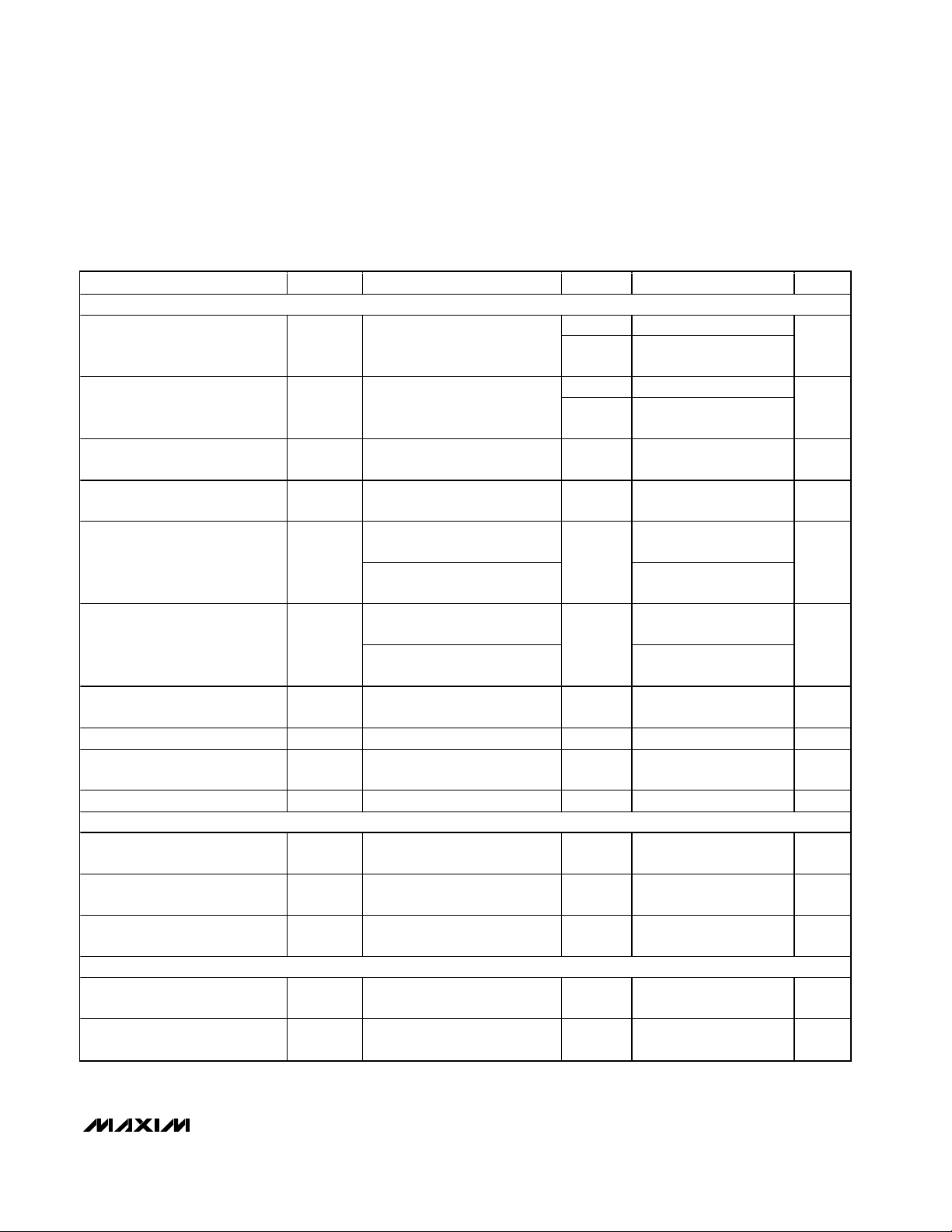
PARAMETER SYMBOL CONDITIONS T
DYNAMIC CHARACTERISTICS
V
, V
Turn-Off Time t
Break-Before-Make Time Delay
(MAX4723 Only) (Note 8)
Skew (Note 8) t
OFF
t
BBM
SKEW
Charge Injection Q
NO_
R
= 300Ω, CL = 35pF, Figure 1
L
V
, V
NO_
= 300Ω, CL = 35pF, Figure 2
R
L
RS = 39Ω, CL = 50pF, Figure 3
V
= 2V, R
GEN
C
= 1.0nF, Figure 4
L
f = 10MHz; V
= 50Ω, CL = 5pF, Figure 5a
R
Off-Isolation (Note 9) V
ISO
L
f = 1MHz; V
= 50Ω, CL = 5pF, Figure 5a
R
L
f = 10MHz; V
= 50Ω, CL = 5pF, Figure 5b
R
Crosstalk (Note 10) V
CT
On-Channel -3dB Bandwidth BW
L
f = 1MHz; V
= 50Ω, CL = 5pF, Figure 5b
R
L
Signal = 0dBm, C
= 50Ω, Figure 5a
R
L
Total Harmonic Distortion THD RL = 600Ω +25°C 0.03 %
C
NO_, NC_ Off-Capacitance
Switch On-Capacitance C
NO_(OFF
C
NC_(OFF
(ON)
f = 1MHz, Figure 6 +25°C9 pF
f = 1MHz, Figure 6 +25°C15 pF
DIGITAL I/O
Input Logic High Voltage V
Input Logic Low Voltage V
Input Leakage Current I
IH
IL
IN
V+ = +3.6V, V
SUPPLY
Supply Voltage Range V+
Positive Supply Current I+ V+ = 5.5V, V
NC_
NC_
= 1.5V;
= 1.5V;
GEN
, V
NO_
, V
NO_
, V
NO_
, V
NO_
= 0 or 5.5V
IN_
= 0V or V+
IN_
A
MIN TYP MAX UNITS
+25°C2040
T
to
MIN
T
MAX
50
+25°C8
T
to
= 0Ω,
NC_
NC_
NC_
NC_
= 5pF,
L
= 1V
= 1V
= 1V
= 1V
P-P
P-P
MIN
T
MAX
T
to
MIN
T
MAX
+25°C5 pC
;
P-P
+25°C
;
;
P-P
+25°C
;
+25°C >300 MHz
T
to
MIN
T
MAX
T
to
MIN
T
MAX
T
to
MIN
T
MAX
T
to
MIN
T
MAX
to
T
MIN
T
MAX
1
0.15 0.2 ns
-55
-80
-80
-110
1.4 V
0.5 V
-0.1 +0.1 µA
1.8 5.5 V
1µA
ns
ns
dB
dB
Page 4
MAX4721/MAX4722/MAX4723
4.5
Ω
Dual SPST Analog Switches in UCSP
4 _______________________________________________________________________________________
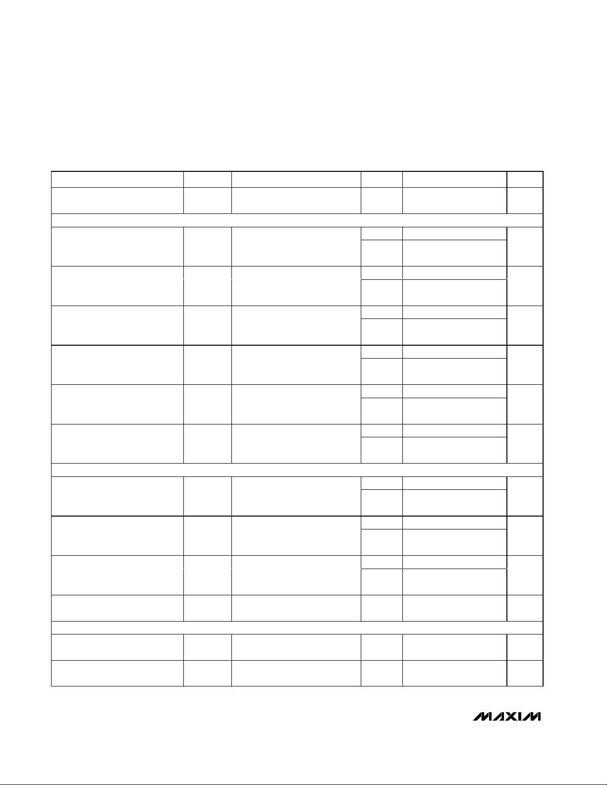
ELECTRICAL CHARACTERISTICS—Single +5V Supply
(V+ = +4.2V to +5.5V, VIH= +2.0V, VIL= +0.8V, TA= T
MIN
to T
MAX
, unless otherwise noted. Typical values are at V+ = +5.0V,
T
A
= +25°C, unless otherwise noted.) (Notes 3, 4)
)
),
)
)
Analog Signal Range
PARAMETER SYMBOL CONDITIONS T
V
,
COM_
V
, V
NO_
NC_
ANALOG SWITCH
On-Resistance (Note 5) R
On-Resistance Match Between
Channels (Notes 5, 6)
On-Resistance Flatness (Note 7) R
NO_, NC_ Off-Leakage Current
(Note 8)
COM _ Off-Leakage Current
(Note 8)
COM_ On-Leakage Current
(Note 8)
∆R
FLAT(ON
I
NO_(OFF
I
NC_(OFF
I
C OM _( OF F )
I
COM_(ON
ON
ON
V+ = 4.2V, I
or V
V
NO_
V+ = 4.2V, I
or V
V
NO_
V+ = 4.2V, I
V
or V
NO_
V+ = 5.5V, V
or V
V
NO_
V+ = 5.5V, V
V
or V
NO_
V+ = 5.5V, V
V
or V
NO_
floating
DYNAMIC CHARACTERISTICS
V
, V
Turn-On Time t
Turn-Off Time t
Break-Before-Make Time Delay
(MAX4723 Only) (Note 8)
Skew (Note 8) t
ON
OFF
t
BBM
SKEW
NO_
R
= 300Ω, CL = 35pF, Figure 1
L
V
, V
NO_
= 300Ω, CL = 35pF, Figure 1
R
L
V
, V
NO_
= 300Ω, CL = 35pF, Figure 2
R
L
RS = 39Ω, CL = 50pF, Figure 3
DIGITAL I/O
Input Logic High Voltage V
Input Logic Low Voltage V
IH
IL
NC_
NC_
NC_
= 10mA;
COM_
= 3.5V
NC_
= 10mA;
COM_
= 3.5V
NC_
= 10mA;
COM_
= 1.0V, 2.0V, 3.5V
NC_
= 1.0V, 4.5V;
COM_
= 4.5V, 1.0V
NC_
= 1V, 4.5V;
COM_
= 4.5V, 1V
NC_
= 1.0V, 4.5V;
COM_
= 1.0V, 4.5V, or
NC_
= 3.0V;
= 3.0V;
= 3.0V;
MIN TYP MAX UNITS
to
0V+V
T
MIN
T
A
MAX
+25°C 1.7 3.0
T
MIN
T
MAX
to
3.5
Ω
+25°C 0.1 0.3
T
MIN
T
MAX
to
0.4
Ω
+25°C 0.4 1.2
T
MIN
T
MAX
to
1.5
Ω
+25°C -0.5 +0.01 +0.5
T
MIN
T
MAX
to
-1.5 +1.5
nA
+25°C -0.5 +0.01 +0.5
T
MIN
T
MAX
to
-1.5 +1.5
nA
+25°C -1 +0.01 +1
T
MIN
T
MAX
to
-2 +2
nA
+25°C3080
T
MIN
T
MAX
to
90
ns
+25°C2040
T
MIN
T
MAX
to
50
ns
+25°C8
T
T
T
T
MIN
T
MIN
T
MIN
T
MIN
T
MAX
MAX
MAX
MAX
to
to
to
1
1.5 2 ns
2.0 V
to
0.8 V
ns
Page 5
MAX4721/MAX4722/MAX4723
4.5
Ω
Dual SPST Analog Switches in UCSP
_______________________________________________________________________________________ 5
ELECTRICAL CHARACTERISTICS—Single +5V Supply (continued)
(V+ = +4.2V to +5.5V, VIH= +2.0V, VIL= +0.8V, TA= T
MIN
to T
MAX
, unless otherwise noted. Typical values are at V+ = +5.0V,
T
A
= +25°C, unless otherwise noted.) (Notes 3, 4)
Note 3: UCSP parts are 100% tested at +25°C only, and guaranteed by design over the specified temperature range. µMAX parts
are 100% tested at T
MAX
and guaranteed by design over the specified temperature range.
Note 4: The algebraic convention used in this data sheet is where the most negative value is a minimum and the most positive
value is a maximum.
Note 5: Guaranteed by design for UCSP parts.
Note 6: ∆R
ON
= R
ON(MAX)
- R
ON(MIN)
.
Note 7: Flatness is defined as the difference between the maximum and minimum value of on-resistance as measured over the
specified analog signal ranges.
Note 8: Guaranteed by design.
Note 9: Off-Isolation = 20log
10(VCOM
/ VNO), V
COM
= output, VNO= input to off switch.
Note 10: Between any two switches.
ON-RESISTANCE vs. V
COM
MAX4721/22/23 toc01
V
COM
(V)
R
ON
(Ω)
4321
2
4
6
8
10
0
05
V+ = 1.8V
V+ = 2.5V
V+ = 3V
V+ = 4.2V
V+ = 5V
ON-RESISTANCE vs. V
COM
MAX4721/22/23 toc02
V
COM
(V)
R
ON
(Ω)
2.52.01.51.00.5
2
3
4
5
6
1
0 3.0
TA = +85°C
TA = +25°C
TA = -40°C
V+ = 3V
ON-RESISTANCE vs. V
COM
MAX4721/22/23 toc03
V
COM
(V)
R
ON
(Ω)
4321
1
2
3
4
5
0
05
V+ = 5V
TA = +85°C
TA = -40°C
TA = +25°C
Typical Operating Characteristics
(TA = +25°C, unless otherwise noted.)
Input Leakage Current I
PARAMETER SYMBOL CONDITIONS T
V+ = 5.5V, VIN_ = 0V or V+
IN
POWER SUPPLY
Power-Supply Range V+
Positive Supply Current I+ V+ = 5.5V, V
= 0V or V+
IN_
MIN TYP MAX UNITS
to
-0.1 +0.1 µA
to
1.8 5.5 V
to
1µA
T
T
T
MIN
T
MIN
T
MIN
T
A
MAX
MAX
MAX
Page 6

MAX4721/MAX4722/MAX4723
4.5
Ω
Dual SPST Analog Switches in UCSP
6 _______________________________________________________________________________________
Typical Operating Characteristics (continued)
(TA = +25°C, unless otherwise noted.)
LEAKAGE CURRENT vs. TEMPERATURE
MAX4721/22/23 toc04a
TEMPERATURE (°C)
LEAKAGE CURRENT (pA)
603510-15
100
200
300
400
500
0
-40 85
V+ = 3V
COM ON-LEAKAGE
COM OFF-LEAKAGE
LEAKAGE CURRENT vs. TEMPERATURE
MAX4721/22/23 toc04b
TEMPERATURE (°C)
LEAKAGE CURRENT (pA)
603510-15
200
400
600
800
1000
0
-40 85
V+ = 5V
COM ON-LEAKAGE
COM OFF-LEAKAGE
CHARGE INJECTION vs. V
COM
MAX4721/22/23 toc05
V
COM
(V)
CHARGE INJECTION (pC)
4321
10
20
30
40
50
0
05
CL = 1nF
V+ = 5V
CL = 1nF
V+ = 3V
SUPPLY CURRENT vs. TEMPERATURE
MAX4721/22/23 toc06
TEMPERATURE (°C)
SUPPLY CURRENT (nA)
603510-15
1
2
3
4
5
6
0
-40 85
V+ = 5V
V+ = 3V
SUPPLY CURRENT vs. LOGIC LEVEL
MAX4721/22/23 toc07
LOGIC LEVEL (V)
SUPPLY CURRENT (µA)
4321
20
40
60
80
100
0
05
V+ = 5V
V+ = 3V
TURN-ON/OFF TIME
vs. SUPPLY VOLTAGE
MAX4721/22/23 toc08
SUPPLY VOLTAGE (V)
t
ON
/t
OFF
(ns)
4.53.52.5
20
40
60
80
100
0
1.5 5.5
t
ON
t
OFF
TURN-ON/OFF TIME
vs. TEMPERATURE
MAX4721/22/23 toc09
TEMPERATURE (°C)
t
ON
/t
OFF
(ns)
603510-15
0
-40 85
t
OFF
, V+ = 3.0V
t
OFF
, V+ = 5.0V
tON, V+ = 5.0V
10
20
30
40
50
60
tON, V+ = 3.0V
RISE/FALL-TIME DELAY
vs. SUPPLY VOLTAGE
MAX4721/22/23 toc10
SUPPLY VOLTAGE (V)
OUTPUT RISE/FALL-TIME DELAY (ps)
4.53.52.5
0.5
1.0
1.5
2.0
2.5
3.0
0
1.5 5.5
INPUT RISE/FALL TIME = 15ns
FIGURE 3, C
L
= 50pF
RISE DELAY
FALL DELAY
RISE/FALL-TIME DELAY
vs. TEMPERATURE
MAX4721/22/23 toc11
TEMPERATURE (°C)
OUTPUT RISE/FALL-TIME DELAY (ns)
603510-15
0.5
1.0
1.5
2.0
0
-40 85
INPUT RISE/FALL TIME = 15ns
FIGURE 3, C
L
= 50pF
V+ = 4.2V
RISE DELAY
FALL DELAY
Page 7

MAX4721/MAX4722/MAX4723
4.5
Ω
Dual SPST Analog Switches in UCSP
_______________________________________________________________________________________ 7
Typical Operating Characteristics (continued)
(TA = +25°C, unless otherwise noted.)
RISE TIME TO FALL TIME MISMATCH
vs. SUPPLY VOLTAGE
400
INPUT RISE/FALL TIME = 15ns
FIGURE 3, C
300
200
MISMATCH (ps)
100
0
1.5 5.5
= 50pF
L
SUPPLY VOLTAGE (V)
4.53.52.5
SKEW vs. TEMPERATURE
200
INPUT RISE/FALL TIME = 15ns
FIGURE 3, C
V+ = 4.2V
150
100
SKEW (ps)
50
0
-40 85
= 50pF
L
TEMPERATURE (°C)
RISE TIME TO FALL TIME MISMATCH
MAX4721/22/23 toc12
MISMATCH (ps)
603510-15
200
vs. TEMPERATURE
INPUT RISE/FALL TIME = 15ns
FIGURE 3, C
V+ = 4.2V
150
100
50
0
-40 85
MAX4721/22/23 toc15
= 50pF
L
TEMPERATURE (°C)
603510-15
400
300
MAX4721/22/23 toc13
200
SKEW (ps)
100
FREQUENCY RESPONSE
20
V+ = 3V/5V
0
-20
-40
-60
ON-LOSS (dB)
-80
-100
-120
-140
ON-LOSS
OFF-ISOLATION
0.0001 100
FREQUENCY (MHz)
SKEW vs. SUPPLY VOLTAGE
INPUT RISE/FALL TIME = 15ns
FIGURE 3, C
0
1.5 5.5
= 50pF
L
SUPPLY VOLTAGE (V)
CROSSTALK
10.01
MAX4721/22/23 toc14
4.53.52.5
MAX4721/22/23 toc16
TOTAL HARMONIC DISTORTION
vs. FREQUENCY
1
V+ = 3V
= 600Ω
R
L
0.1
THD (%)
0.01
10 100k
LOGIC THRESHOLD vs. SUPPLY VOLTAGE
2.0
1.6
MAX4721/22/23 toc17
10k1k100
1.2
0.8
LOGIC THRESHOLD (V)
0.4
0
1.5 5.5
SUPPLY VOLTAGE (V)
MAX4721/22/23 toc18
V
TH+
V
TH-
5.04.54.03.53.02.52.0
Page 8

MAX4721/MAX4722/MAX4723
4.5
Ω
Dual SPST Analog Switches in UCSP
8 _______________________________________________________________________________________
Detailed Description
The MAX4721/MAX4722/MAX4723 dual SPST analog
switches operate from a single +1.8V to +5.5V supply.
The MAX4721/MAX4722/MAX4723 offer excellent AC
characteristics, <0.5nA leakage current, less than 2ms
differential skew, and 15pF on-channel capacitance. All
of these devices are CMOS-logic compatible with railto-rail signal handling capability.
The MAX4721/MAX4722/MAX4723 are USB-compliant
switches that provide 4.5Ω (max) on-resistance, and
15pF on-channel capacitance to maintain signal integrity. At 12Mbps (USB full-speed data rate specification)
the MAX4721/MAX4722/MAX4723 introduce less than
2ns propagation delay between input and output signals and less than 0.5ns change in skew for the output
signals (see Figure 3 for more details).
The MAX4721 has two normally open (NO) switches, the
MAX4722 has two normally closed (NC) switches, and
the MAX4723 has one NO switch and one NC switch.
Applications Information
Digital Control Inputs
The MAX4721/MAX4722/MAX4723 logic inputs accept
up to +5.5V regardless of supply voltage. For example,
with a +3.3V supply, IN_ can be driven low to GND and
high to +5.5V allowing for mixing of logic levels in a
system. Driving the control logic inputs rail-to-rail minimizes power consumption. For a +3.0V supply voltage,
the logic thresholds are 0.5V (low) and 1.4V (high); for
a +5V supply voltage, the logic thresholds are 0.8V
(low) and 2.0V (high).
Analog Signal Levels
Analog signals that range over the entire supply voltage
(V+ to GND) are passed with very little change in on-resistance (see the Typical Operating Characteristics). The
switches are bidirectional, so the NO_, NC_, and COM_
pins can be either inputs or outputs.
Pin Description
PIN
MAX4721
UCSP µMAX UCSP µMAX UCSP µMAX
A1 3 A1 3 A1 3 IN2 Logic-Control Digital Input
A2 4 A2 4 A2 4 GND Ground. Connect to digital ground.
A3 5 —— — —NO2 Analog-Switch Normally Open Terminal
B1 2 B1 2 B1 2 COM1 Analog-Switch Common Terminal
B3 6 B3 6 B3 6 COM2 Analog-Switch Common Terminal
C1 1 ——C1 1 NO1 Analog-Switch Normally Open Terminal
C2 8 C2 8 C2 8 V+ Positive Analog Supply
C3 7 C3 7 C3 7 IN1 Logic-Control Digital Input
——C1 1 ——NC1 Analog-Switch Normally Closed Terminal
——A3 5 A3 5 NC2 Analog-Switch Normally Closed Terminal
MAX4722 MAX4723
NAME
FUNCTION
Page 9

Power-Supply Bypassing
Power-supply bypassing improves noise margin and
prevents switching noise from propagating from the V+
supply to other components. A 0.1µF capacitor connected from V+ to GND is adequate for most applications.
Power-Supply Sequencing
and Overvoltage Protection
Caution: Do not exceed the absolute maximum ratings because stresses beyond the listed ratings may
cause permanent damage to the device.
UCSP Package Considerations
For general UCSP package information and PC layout
considerations, please refer to the Maxim Application
Note (Wafer-Level Chip-Scale Package).
UCSP Reliability
The chip-scale package (UCSP) represents a unique
packaging form factor that may not perform equally to a
packaged product through traditional mechanical reliability tests. UCSP reliability is integrally linked to the
user’s assembly methods, circuit board material, and
usage environment. The user should closely review
these areas when considering use of a UCSP package.
Performance through Operating Life Test and Moisture
Resistance remains uncompromised as it is primarily
determined by the wafer-fabrication process.
Mechanical stress performance is a greater consideration for a UCSP package. UCSPs are attached through
direct solder contact to the user’s PC board, foregoing
the inherent stress relief of a packaged product lead
frame. Solder joint contact integrity must be considered. Information on Maxim’s qualification plan, test
data, and recommendations are detailed in the UCSP
application note, which can be found on Maxim’s website at www.maxim-ic.com.
MAX4721/MAX4722/MAX4723
4.5
Ω
Dual SPST Analog Switches in UCSP
_______________________________________________________________________________________ 9
Test Circuits/Timing Diagrams
Figure 1. Switching Time
Figure 2. Break-Before-Make Interval
MAX4721/
MAX4722/
MAX4723
LOGIC
INPUT
V
N_
MAX4723
V
LOGIC
INPUT
COM1
V
COM2
COM1
COM2
IN_
NO_
OR NC_
IN_
GND
GND
V+
V+
COM_
R
L
C
INCLUDES FIXTURE AND STRAY CAPACITANCE.
L
V
= V
OUT
V+
V+
NO_
NC_
C
INCLUDES FIXTURE AND STRAY CAPACITANCE.
L
COM
(
RL - R
R
L
)
ON
V
OUT2
R
C
L2
L2
V
OUT
C
L
V
OUT1
R
L1 C
V
LOGIC
INPUT
(V
OUT1
(V
OUT2
IH
V
IL
0V
V
IH
V
IL
)
0V
)
0V
50%
t
OFF
V
OUT
0.9 x V
0UT
t
ON
LOGIC INPUT WAVEFORMS INVERTED FOR SWITCHES
THAT HAVE THE OPPOSITE LOGIC SENSE.
50%
0.9 x V
0UT1
t
D
0.9 x V
OUT
0.9 x V
OUT2
t
D
LOGIC
INPUT
SWITCH
OUTPUT
SWITCH
OUTPUT 1
L1
SWITCH
OUTPUT 2
Page 10

MAX4721/MAX4722/MAX4723
4.5
Ω
Dual SPST Analog Switches in UCSP
10 ______________________________________________________________________________________
Figure 3. Input/Output Skew Timing Diagram
Test Circuits/Timing Diagrams (continued)
t
ri
90%
t
fi
t
ro
50%
t
fo
50%
50%
50%
t
skew_i
10%
90%
t
skew_o
10%
TxD+
TxD-
Rs = 39Ω
= 50pF
C
L
A
R
s
A-
R
s
B
B-
C
C
L
L
INPUT A
INPUT A-
OUTPUT B
OUTPUT B-
10%
90%
10%
90%
|
DELAY DUE TO SWITCH FOR RISING INPUT AND RISING OUTPUT SIGNALS.
|t
ro - tri
|t
|
DELAY DUE TO SWITCH FOR FALLING INPUT AND FALLING OUTPUT SIGNALS.
fo - tfi
|t
|
CHANGE IN SKEW THROUGH THE SWITCH FOR OUTPUT SIGNALS.
skew_o
|t
|
CHANGE IN SKEW THROUGH THE SWITCH FOR INPUT SIGNALS.
skew_i
Page 11

MAX4721/MAX4722/MAX4723
4.5
Ω
Dual SPST Analog Switches in UCSP
______________________________________________________________________________________ 11
Figure 4. Charge Injection
Figure 5a. On-Loss, Off-Isolation, and Crosstalk
Figure 5b. Crosstalk Test Circuit
Figure 6. Channel Off/On-Capacitance
Test Circuits/Timing Diagrams (continued)
Chip Information
TRANSISTOR COUNT: 181
PROCESS: BiCMOS
MAX4721/
MAX4722/
MAX4723
V
GEN
R
GEN
C = 0.1µF
SIGNAL
GENERATOR
0dBm
50Ω*
ANALYZER
NC_
OR NO_
GND
V+
V+
NC_ or NO_
COM_
IN_
V
IL
MAX4721/
MAX4722/
MAX4723
GND
COM_
TO V
V+
V+
IH
IN_
∆V
OUT
V
OUT
V
C
L
0V OR V+
OUT
IN
OFF
OFF
IN
SIGNAL GENERATOR
0dBm
0V TO V+
ANALYZER
ON
ON
Q = (∆V
LOGIC INPUT WAVEFORMS INVERTED FOR SWITCHES
THAT HAVE THE OPPOSITE LOGIC SENSE.
C = 0.1µF
OUT
)(CL)
V+
OFF
OFF
MAX4721/
MAX4722/
MAX4723
V+
COM1
IN1
NO2
GND
NO1
IN2
COM2
50Ω
0V OR V+
N.C.
*USED ONLY FOR OFF-ISOLATION TEST.
C = 0.1µF
V+
V+
NC_ or NO_
MAX4721/
MAX4722/
MAX4723
CAPACITANCE
METER
f = 1MHz
COM_
GND
IN_
0V OR V+
Page 12

MAX4721/MAX4722/MAX4723
4.5
Ω
Dual SPST Analog Switches in UCSP
12 ______________________________________________________________________________________
Pin Configurations/Functional Diagrams/Truth Tables (continued)
TOP VIEW
NO1
COM1
IN2
MAX4721
1
2
3
4
µMAX
LOGIC SWITCH
0
1
OFF
ON
V+
8
IN1
7
COM2
6
NO2GND
5
NC1
COM1
IN2
SWITCHES SHOWN FOR LOGIC "0" INPUT
MAX4722
1
2
3
4
µMAX
LOGIC SWITCH
0
1
8
7
6
5
ON
OFF
V+
IN1
COM2
NC2GND
NO1
1
COM1
2
IN2
3
4
LOGIC SWITCH1
0
1
MAX4723
µMAX
OFF
ON
8
7
6
5
SWITCH2
ON
OFF
V+
IN1
COM2
NC2GND
Page 13

MAX4721/MAX4722/MAX4723
4.5
Ω
Dual SPST Analog Switches in UCSP
______________________________________________________________________________________ 13
Package Information
(The package drawing(s) in this data sheet may not reflect the most current specifications. For the latest package outline information,
go to www.maxim-ic.com/packages.)
Page 14

MAX4721/MAX4722/MAX4723
4.5
Ω
Dual SPST Analog Switches in UCSP
Maxim cannot assume responsibility for use of any circuitry other than circuitry entirely embodied in a Maxim product. No circuit patent licenses are
implied. Maxim reserves the right to change the circuitry and specifications without notice at any time.
14 ____________________Maxim Integrated Products, 120 San Gabriel Drive, Sunnyvale, CA 94086 408-737-7600
© 2002 Maxim Integrated Products Printed USA is a registered trademark of Maxim Integrated Products.
Package Information (continued)
(The package drawing(s) in this data sheet may not reflect the most current specifications. For the latest package outline information,
go to www.maxim-ic.com/packages.)
8
b
E H
A1
A
ÿ 0.50±0.1
0.6±0.1
0.6±0.1
1
D
TOP VIEW
A2
e
FRONT VIEW
4X S
BOTTOM VIEW
c
L
SIDE VIEW
8
1
6∞
MILLIMETERS
MIN
0.05 0.15
0.25 0.36
0.13 0.18
2.95 3.05
2.95 3.05
4.78
0.41
MAX
- 1.10
0.950.75
0.65 BSC
5.03
0.66
0.5250 BSC
8LUMAXD.EPS
6∞0∞
DIM
A
A1
A2
b
c
D
e
E
H
L
α
S
INCHES
MIN
-
0.002
0.030
0.010
0.005
0.116
0.0256 BSC
0.116
0.188
0.016
0∞
0.0207 BSC
MAX
0.043
0.006
0.037
0.014
0.007
0.120
0.120
0.198
0.026
α
PROPRIETARY INFORMATION
TITLE:
PACKAGE OUTLINE, 8L uMAX/uSOP
REV.DOCUMENT CONTROL NO.APPROVAL
21-0036
1
J
1
 Loading...