

General Description
The MAX4717/MAX4718 low-voltage, low on-resistance
(RON), dual single-pole/double throw (SPDT) analog
switches operate from a single +1.8V to +5.5V supply.
These devices are designed for USB 1.1 and audio
switching applications.
The MAX4717 features two 4.5Ω RON(max) SPDT
switches with 1.2Ω flatness and 0.3Ω matching between
channels. The MAX4718 features one 4.5Ω RON(max)
SPDT switch and one 20Ω RON(max) SPDT switch. The
20Ω switch has a guaranteed matching and flatness of
0.4Ω and 1.2Ω, respectively. These switches offer breakbefore-make switching (1ns) with tON<80ns and t
OFF
<40ns at +2.7V. The digital logic inputs are +1.8V logic
compatible with a +2.7V to +3.6V supply.
These switches are packaged in a chip-scale package
(UCSP™), significantly reducing the required PC board
area. The chip occupies only a 2.0mm ✕ 1.50mm area
and has a 4 ✕ 3 bump array with a bump pitch of 0.5mm.
These switches are also available in 10-pin µMAX®and
10-pin TDFN packages.
Applications
USB 1.1 Signal Switching Circuits
Battery-Operated Equipment
Audio/Video-Signal Routing
Headphone Switching
Low-Voltage Data-Acquisition Systems
Sample-and-Hold Circuits
Cell Phones
PDAs
Features
♦ USB 1.1 Signal Switching Compliant
(TID = 4000231)
♦ 2ns (max) Differential Skew
♦ -3dB Bandwidth: > 300MHz
♦ Low 15pF On-Channel Capacitance
♦ Single-Supply Operation from +1.8V to +5.5V
♦ 4.5Ω RON(max) Switches (MAX4717/MAX4718)
0.3Ω (max) RONMatch (+3.0V Supply)
1.2Ω (max) Flatness (+3.0V Supply)
♦ 20Ω RON(max) Switch (MAX4718)
0.4Ω (max) RONMatch (+3.0V Supply)
1.2Ω (max) Flatness (+3.0V Supply)
♦ Rail-to-Rail Signal Handling
♦ High Off-Isolation: -55dB (10MHz)
♦ Low Crosstalk: -80dB (10MHz)
♦ Low Distortion: 0.03%
♦ +1.8V CMOS-Logic Compatible
♦ < 0.5nA Leakage Current at +25°C
MAX4717/MAX4718
4.5Ω/20Ω, 300MHz Bandwidth, Dual SPDT
Analog Switches in UCSP
________________________________________________________________ Maxim Integrated Products 1
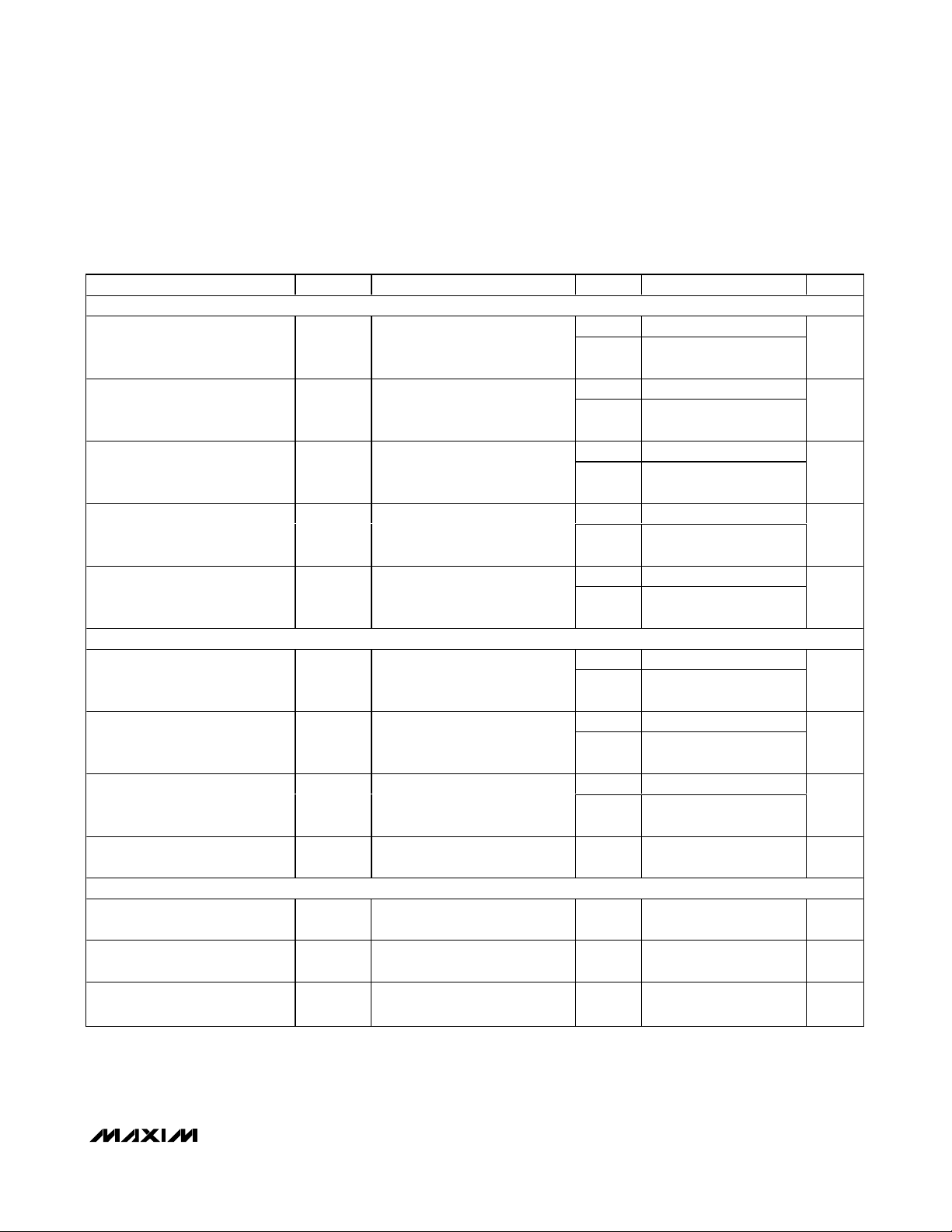
Ordering Information
19-2627; Rev 2; 9/05
For pricing, delivery, and ordering information, please contact Maxim/Dallas Direct! at
1-888-629-4642, or visit Maxim’s website at www.maxim-ic.com.
Pin Configurations/Functional Diagrams/Truth Tables
UCSP is a trademark of Maxim Integrated Products, Inc.
µMAX is a registered trademark of Maxim Integrated Products, Inc.
*EP = Exposed paddle.
PART TEMP RANGE
MAX4717EUB -40°C to +85°C 10 µMAX —
MAX4717ETB -40°C to +85°C 10 TDFN-EP* ACV
MAX4717EBC-T -40°C to +85°C 12 UCSP-12 ABH
MAX4718EUB -40°C to +85°C 10 µMAX —
MAX4718ETB -40°C to +85°C 10 TDFN-EP* ACW
MAX4718EBC-T -40°C to +85°C 12 UCSP-12 ABI
PIN/BUMPPACKAGE
MARK
TOP
TOP VIEW
(BUMP SIDE DOWN)
MAX4717/MAX4718
C1
NC1
C2
C3
C4 B4 A4
GND
V+
UCSP
A1B1
NC2
A2
IN2IN1
COM2COM1
A3
NO2NO1
MAX4717/MAX4718
1
V+
2
NO1
3
COM1
4
IN1
5
NC1
TDFN
PART
10
NO2
9
COM2
8
IN2
7
NC2
6
GND
MAX4717
MAX4718
IN_
SWITCHES SHOWN FOR LOGIC "0" INPUT
SPDT1
4.5Ω
4.5Ω
MAX4717/MAX4718
NO_
0
1
OFF
ON
SPDT2
4.5Ω
20Ω
NC_
ON
OFF
V+
NO1
COM1
IN1
NC1
MAX4717/MAX4718
1
2
3
4
5
µMAX
10
NO2
9
COM2
IN2
8
7
NC2
GND
6
MAX4717/MAX4718
4.5Ω/20Ω, 300MHz Bandwidth, Dual SPDT
Analog Switches in UCSP
2 _______________________________________________________________________________________
ABSOLUTE MAXIMUM RATINGS
ELECTRICAL CHARACTERISTICS—Single +3V Supply
(V+ = +2.7V to +3.6V, VIH= +1.4V, VIL= +0.5V, TA= T
MIN
to T
MAX
, unless otherwise noted. Typical values are at V+ = +3.0V,
T
A
= +25°C, unless otherwise noted.) (Notes 2, 3)
Stresses beyond those listed under “Absolute Maximum Ratings” may cause permanent damage to the device. These are stress ratings only, and functional
operation of the device at these or any other conditions beyond those indicated in the operational sections of the specifications is not implied. Exposure to
absolute maximum rating conditions for extended periods may affect device reliability.
(All voltages are referenced to GND.)
V+, IN_...................................................................-0.3V to +6.0V
COM_, NO_, NC_ (Note 1) ...........................-0.3V to (V+ + 0.3V)
Continuous Current COM_, NO_, NC_ ...........................±100mA
Peak Current COM_, NO_, NC_
(pulsed at 1ms, 10% duty cycle)................................±200mA
Continuous Power Dissipation (T
A
= +70°C)
10-Pin µMAX (derate 5.6mW/°C above +70°C) ...........444mW
10-Pin TDFN (derate 24.4mW/°C above +70°C) .......1951mW
12-Bump UCSP (derate 11.4mW/°C above +70°C) ....909mW
ESD Method 3015.7 .............................................................>2kV
Operating Temperature Range ...........................-40°C to +85°C
Junction Temperature......................................................+150°C
Storage Temperature Range .............................-65°C to +150°C
Lead Temperature (soldering, 10s) .................................+300°C
Bump Temperature (soldering)
Infrared (15s) ...............................................................+220°C
Vapor Phase (60s) .......................................................+215°C
Note 1: Signals on COM_, NO_, or NC_ exceeding V+ or GND are clamped by internal diodes. Limit forward-diode current to
maximum current rating.
)
),
)
)
PARAMETER SYMBOL CONDITIONS T
V
,
Analog Signal Range
V
NO_
COM_
, V
NC_
ANALOG SWITCH (Low RON—MAX4717/MAX4718 SPDT 1)
On-Resistance
(Note 4)
On-Resistance Match Between
Channels (Notes 4, 5)
On-Resistance Flatness
(Note 6)
NO_, NC_ Off-Leakage Current
(Note 7)
COM_ On-Leakage Current
(Note 7)
R
ON
∆R
R
FLAT(ON
I
NO_(OFF
I
NC_(OFF
I
COM_(ON
ON
V+ = 2.7V, I
or V
V
NO_
V+ = 2.7V, I
or V
V
NO_
V+ = 2.7V, I
V
or V
NO_
V+ = 3.6V, V
or V
V
NO_
V+ = 3.6V, V
V
or V
NO_
floating
ANALOG SWITCH (High RON—MAX4718 SPDT 2)
On-Resistance (Note 4) R
ON
V+ = 2.7V, I
or V
V
NO_
= 10mA;
COM_
= 1.5V
NC_
= 10mA;
COM_
= 1.5V
NC_
= 10mA;
COM_
= 1.0V, 1.5V, 2.0V
NC_
= 0.3V, 3.3V;
COM_
= 3.3V, 0.3V
NC_
= 0.3V, 3.3V;
COM_
= 0.3V, 3.3V, or
NC_
= 10mA;
COM_
= 1.5V
NC_
MIN TYP MAX UNITS
to
0V+V
T
MIN
T
A
MAX
+25°C 3.0 4.5
T
to
MIN
T
MAX
5
+25°C 0.1 0.3
T
to
MIN
T
MAX
0.4
+25°C 0.6 1.2
T
to
MIN
T
MAX
1.5
+25°C -0.5 +0.01 +0.5
T
to
MIN
T
MAX
-1 +1
+25°C -1 +0.01 +1
to
T
MIN
T
MAX
-2 +2
+25°C 15 20
T
to
MIN
T
MAX
25
Ω
Ω
Ω
nA
nA
Ω
MAX4717/MAX4718
4.5Ω/20Ω, 300MHz Bandwidth, Dual SPDT
Analog Switches in UCSP
_______________________________________________________________________________________ 3
ELECTRICAL CHARACTERISTICS—Single +3V Supply (continued)
(V+ = +2.7V to +3.6V, VIH= +1.4V, VIL= +0.5V, TA= T
MIN
to T
MAX
, unless otherwise noted. Typical values are at V+ = +3.0V,
T
A
= +25°C, unless otherwise noted.) (Notes 2, 3)
)
),
)
)
),
)
PARAMETER SYMBOL CONDITIONS T
On-Resistance Match Between
Channels (Notes 4, 5)
On-Resistance Flatness
(Note 6)
NO_, NC_ Off-Leakage Current
(Note 7)
COM_ On-Leakage Current
(Note 7)
∆R
R
FLAT(ON
I
NO_(OFF
I
NC_(OFF
I
COM_(ON
ON
V+ = 2.7V, I
V
or V
NO_
V+ = 2.7V, I
or V
V
NO_
V+ = 3.6V, V
or V
V
NO_
V+ = 3.6V, V
V
or V
NO_
floating
DYNAMIC CHARACTERISTICS
V
, V
Turn-On Time t
Turn-Off Time t
Break-Before-Make Time Delay
(Note 7)
Skew (Note 7) t
OFF
t
BBM
SKEW
Charge Injection Q
ON
NO_
R
= 300Ω, CL = 35pF, Figure 1;
L
= 1.5V, VIL = 0V
V
IH
V
, V
NO_
R
= 300Ω, CL = 35pF, Figure 1;
L
= 1.5V, VIL = 0V
V
IH
V
, V
NO_
= 300Ω, CL = 35pF, Figure 2
R
L
RS = 39Ω, CL = 50pF, Figure 3
V
GEN
C
= 1.0nF, Figure 4
L
f = 10MHz; V
R
= 50Ω, CL = 5pF, Figure 5
Off-Isolation V
ISO
L
f = 1MHz; V
= 50Ω, CL = 5pF, Figure 5
R
L
f = 10MHz; V
= 50Ω, CL = 5pF, Figure 5
R
Crosstalk (Note 8) V
CT
On-Channel -3dB Bandwidth BW
Total Harmonic Distortion THD V
C
NO_, NC_ Off-Capacitance
NO_(OFF
C
NC_(OFF
L
f = 1MHz; V
= 50Ω, CL = 5pF, Figure 5
R
L
Signal = 0dBm, R
= 5pF, Figure 5
C
L
COM_
f = 1MHz, Figure 6 +25°C 9 pF
COM_
NC_
COM_
NC_
COM_
NC_
COM_
NC_
= 1.5V;
NC_
= 1.5V;
NC_
= 1.5V;
NC_
= 1.5V, R
NO_
NO_
NO_
NO_
= 2V
P-P
A
MIN TYP MAX UNITS
+25°C 0.15 0.4
= 10mA;
= 1.5V
T
MIN
T
to
MAX
+25°C 0.6 1.2
= 10mA;
= 1.0V, 1.5V, 2.0V
T
MIN
T
to
MAX
+25°C -0.5 +0.01 +0.5
= 0.3V, 3.3V;
= 3.3V, 0.3V
= 0.3V, 3.3V;
= 0.3V, 3.3V, or
T
to
MIN
T
MAX
+25°C -1 +0.01 +1
to
T
MIN
T
MAX
+25°C 40 80
to
T
MIN
T
MAX
+25°C 20 40
T
to
MIN
T
MAX
+25°C 8
T
to
MIN
T
MAX
T
to
MIN
T
MAX
= 0Ω,
GEN
, V
NC_
= 1V
+25°C 5 pC
;
P-P
+25°C
, V
, V
NC_
NC_
= 1V
= 1V
P-P
P-P
;
;
+25°C
, V
NC_
= 50Ω,
L
= 1V
P-P
;
+25°C >300 MHz
, RL = 600Ω +25°C 0.03 %
0.5
1.5
-1 +1
-2 +2
100
50
1
0.15 2 ns
-55
-80
-80
-110
Ω
Ω
nA
nA
ns
ns
ns
dB
dB
MAX4717/MAX4718
4.5Ω/20Ω, 300MHz Bandwidth, Dual SPDT
Analog Switches in UCSP
4 _______________________________________________________________________________________
ELECTRICAL CHARACTERISTICS—Single +3V Supply (continued)
(V+ = +2.7V to +3.6V, VIH= +1.4V, VIL= +0.5V, TA= T
MIN
to T
MAX
, unless otherwise noted. Typical values are at V+ = +3.0V,
T
A
= +25°C, unless otherwise noted.) (Notes 2, 3)
ELECTRICAL CHARACTERISTICS—Single +5V Supply
(V+ = +4.2V to +5.5V, VIH= +2.0V, VIL= +0.8V, TA= T
MIN
to T
MAX
, unless otherwise noted. Typical values are at V+ = +5.0V,
T
A
= +25°C, unless otherwise noted.) (Notes 2, 3)
)
),
)
)
PARAMETER SYMBOL CONDITIONS T
Switch On-Capacitance C
(ON)
f = 1MHz, Figure 6 +25°C 15 pF
DIGITAL I/O
Input Logic High Voltage V
Input Logic Low Voltage V
Input Leakage Current I
IH
IL
IN
V+ = +3.6V, V
POWER SUPPLY
Power-Supply Range V+
Supply Current I+ V+ = +5.5V, V
= 0 or 5.5V
IN_
= 0V or V+
IN_
MIN TYP MAX UNITS
to
1.4 V
to
to
-100 +100 nA
to
1.8 5.5 V
to
T
T
T
T
T
MIN
T
MIN
T
MIN
T
MIN
T
MIN
T
A
MAX
MAX
MAX
MAX
MAX
0.5 V
1µA
PARAMETER SYMBOL CONDITIONS T
V
,
Analog Signal Range
V
NO_
COM_
, V
NC_
ANALOG SWITCH (Low RON—MAX4717/MAX4718 SPDT 1)
ON
V+ = 4.2V, I
V
NO_
V+ = 4.2V, I
V
NO_
V+ = 4.2V, I
V
NO_
V+ = 5.5V; V
V
NO_
V+ = 5.5V; V
V
NO_
floating
On-Resistance (Note 4) R
On-Resistance Match Between
Channels (Notes 4, 5)
On-Resistance Flatness
(Note 6)
NO_, NC_ Off-Leakage Current
(Note 7)
COM_ On-Leakage Current
(Note 7)
R
FLAT(ON
I
NO_(OFF
I
NC_(OFF
I
COM_(ON
ON
∆R
or V
or V
or V
or V
or V
= 10mA;
COM_
= 3.5V
NC_
= 10mA;
COM_
= 3.5V
NC_
= 10mA;
COM_
= 1.0V, 2.0V, 3.5V
NC_
= 1.0V, 4.5V;
COM_
= 1.0V, 4.5V
NC_
= 1.0V, 4.5V;
COM_
= 1.0V, 4.5V, or
NC_
MIN TYP MAX UNITS
to
0V+V
T
MIN
T
A
MAX
+25°C 1.7 3
T
to
MIN
T
MAX
3.5
+25°C 0.1 0.3
T
to
MIN
T
MAX
0.4
+25°C 0.4 1.2
T
to
MIN
T
MAX
1.5
+25°C -0.5 +0.01 +0.5
T
to
MIN
T
MAX
-1 +1
+25°C -1 +0.01 +1
to
T
MIN
T
MAX
-2 +2
Ω
Ω
Ω
nA
nA
MAX4717/MAX4718
4.5Ω/20Ω, 300MHz Bandwidth, Dual SPDT
Analog Switches in UCSP
_______________________________________________________________________________________ 5
ELECTRICAL CHARACTERISTICS—Single +5V Supply (continued)
(V+ = +4.2V to +5.5V, VIH= +2.0V, VIL= +0.8V, TA= T
MIN
to T
MAX
, unless otherwise noted. Typical values are at V+ = +5.0V,
T
A
= +25°C, unless otherwise noted.) (Notes 2, 3)
)
),
)
)
PARAMETER SYMBOL CONDITIONS T
ANALOG SWITCH (High RON—MAX4718 SPDT 2)
ON
V+ = 4.2V, I
V
NO_
V+ = 4.2V, I
V
NO_
V+ = 4.2V, I
V
NO_
V+ = 5.5V; V
V
NO_
V+ = 5.5V, V
V
NO_
floating
On-Resistance (Note 4) R
On-Resistance Match Between
Channels (Notes 4, 5)
On-Resistance Flatness
(Note 6)
NO_, NC_ Off-Leakage Current
(Note 7)
COM_ On-Leakage Current
(Note 7)
R
FLAT(ON
I
NO_(OFF
I
NC_(OFF
I
COM_(ON
ON
∆R
DYNAMIC CHARACTERISTICS
V
Turn-On Time t
Turn-Off Time t
Break-Before-Make Time Delay
(Note 7)
Skew (Note 7) t
ON
OFF
t
BBM
SKEW
NO_
R
= 300Ω, CL = 35pF, Figure 1
L
V
NO_
R
= 300Ω, CL = 35pF, Figure 1
L
V
NO_
= 300Ω, CL = 35pF, Figure 2
R
L
RS = 39Ω, CL = 50pF, Figure 3
DIGITAL I/O
Input Logic High Voltage V
Input Logic Low Voltage V
Input Leakage Current I
IH
IL
IN
V+ = 5.5V, VIN_ = 0V or V+
or V
or V
or V
or V
or V
, V
, V
, V
NC_
NC_
NC_
= 10mA;
COM_
= 3.5V
NC_
= 10mA;
COM_
= 3.5V
NC_
= 10mA;
COM_
= 1.0V, 2.0V, 4.5V
NC_
= 1.0V, 4.5V;
COM_
= 1.0V, 4.5V
NC_
= 1.0V, 4.5V;
COM_
= 1.0V, 4.5V, or
NC_
= 3.0V;
= 3.0V;
= 3.0V;
A
MIN TYP MAX UNITS
+25°C 12 20
T
to
MIN
T
MAX
+25°C 0.15 0.4
T
to
MIN
T
MAX
+25°C 0.4 1.2
T
to
MIN
T
MAX
+25°C -0.5 +0.01 +0.5
T
to
MIN
T
MAX
+25°C -1 +0.01 +1
to
T
MIN
T
MAX
+25°C 30 80
T
to
MIN
T
MAX
+25°C 20 40
T
to
MIN
T
MAX
+25°C 8
T
to
MIN
T
MAX
T
to
MIN
T
MAX
T
to
T
T
MIN
T
MIN
T
MIN
T
MAX
MAX
MAX
2.0 V
to
to
-100 +100 nA
25
0.5
1.5
-1 +1
-2 +2
100
50
1
0.15 2 ns
0.8 V
Ω
Ω
Ω
nA
nA
ns
ns
ns

MAX4717/MAX4718
4.5Ω/20Ω, 300MHz Bandwidth, Dual SPDT
Analog Switches in UCSP
6 _______________________________________________________________________________________
Note 2: UCSP and TDFN parts are 100% tested at +25°C only, and guaranteed by design over the specified temperature range.
µMAX parts are 100% tested at T
MAX
and guaranteed by design over the specified temperature range.
Note 3: The algebraic convention used in this data sheet is where the most negative value is a minimum and the most positive
value is a maximum.
Note 4: Guaranteed by design for UCSP and TDFN parts.
Note 5: ∆R
ON
= R
ON(MAX)
- R
ON(MIN)
.
Note 6: Flatness is defined as the difference between the maximum and minimum value of on-resistance as measured over the
specified analog signal ranges.
Note 7: Guaranteed by design.
Note 8: Between any two switches.
ELECTRICAL CHARACTERISTICS—Single +5V Supply (continued)
(V+ = +4.2V to +5.5V, VIH= +2.0V, VIL= +0.8V, TA= T
MIN
to T
MAX
, unless otherwise noted. Typical values are at V+ = +5.0V,
T
A
= +25°C, unless otherwise noted.) (Notes 2, 3)
Typical Operating Characteristics
(TA = +25°C, unless otherwise noted.)
PARAMETER SYMBOL CONDITIONS T
POWER SUPPLY
Power-Supply Range V+
Supply Current I+ V+ = 5.5V, V
= 0V or V+
IN_
MIN TYP MAX UNITS
to
1.8 5.5 V
to
1µA
T
T
MIN
T
MIN
T
A
MAX
MAX
ON-RESISTANCE vs. COM_ VOLTAGE
10
LOW RON SWITCH
8
6
(Ω)
ON
R
4
2
0
05
V+ = 1.8V
V+ = 2.5V
V
COM_
V+ = 3V
(V)
V+ = 4.2V
V+ = 5V
4321
MAX4717/18 toc01
(Ω)
R
ON-RESISTANCE vs. COM_ VOLTAGE
6
V+ = 3V
SWITCH
LOW R
ON
5
4
ON
TA = +25°C
3
2
1
03.0
TA = -40°C
V
COM_
TA = +85°C
(V)
MAX4717/18 toc02
2.52.01.51.00.5
ON-RESISTANCE vs. COM_ VOLTAGE
5
V+ = 5V
LOW RON SWITCH
4
3
(Ω)
R
TA = +25°C
ON
2
1
TA = -40°C
0
05
TA = +85°C
V
_ (V)
COM
MAX4717/18 toc03
4321

MAX4717/MAX4718
4.5Ω/20Ω, 300MHz Bandwidth, Dual SPDT
Analog Switches in UCSP
_______________________________________________________________________________________ 7
Typical Operating Characteristics (continued)
(TA = +25°C, unless otherwise noted.)
ON-RESISTANCE vs. COM_ VOLTAGE
20
V+ = 1.8V
18
16
(Ω)
ON
R
14
12
10
05
V+ = 2.5V
V
COM
HIGH RON SWITCH
V+ = 4.2V
V+ = 5V
4321
_ (V)
LEAKAGE CURRENT vs. TEMPERATURE
500
V+ = 3V
SWITCH
LOW R
400
ON
MAX4717/18 toc04
MAX4717/18 toc07
ON-RESISTANCE vs. COM_ VOLTAGE
15
V+ = 3V
SWITCH
HIGH R
14
13
(Ω)
ON
R
12
11
10
ON
TA = +25°C
0 3.0
V
COM
TA = +85°C
TA = -40°C
_ (V)
LEAKAGE CURRENT vs. TEMPERATURE
1000
V+ = 5V
SWITCH
LOW R
800
ON
MAX4717/18 toc05
2.52.01.51.00.5
MAX4717/18 toc08
ON-RESISTANCE vs. COM_ VOLTAGE
15
V+ = 5V
HIGH RON SWITCH
14
TA = -40°C
V
COM
TA = +85°C
_ (V)
13
(Ω)
ON
R
12
11
10
05
LEAKAGE CURRENT vs. TEMPERATURE
700
V+ = 3V
SWITCH
HIGH R
ON
500
COM_ ON-LEAKAGE
MAX4717/18 toc06
TA = +25°C
4321
MAX4717/18 toc09
300
COM_ OFF-LEAKAGE
200
LEAKAGE CURRENT (pA)
100
0
-40 85
COM_ ON-LEAKAGE
TEMPERATURE (°C)
LEAKAGE CURRENT vs. TEMPERATURE
900
V+ = 5V
SWITCH
HIGH R
700
500
300
LEAKAGE CURRENT (pA)
100
-100
ON
COM_ ON-LEAKAGE
COM_ OFF-LEAKAGE
-40 85
TEMPERATURE (°C)
600
COM_ OFF-LEAKAGE
400
LEAKAGE CURRENT (pA)
200
0
603510-15
-40 85
CHARGE INJECTION vs. V
50
40
MAX4717/18 toc10
30
20
CHARGE INJECTION (pC)
10
0
603510-15
05
COM_ ON-LEAKAGE
TEMPERATURE (°C)
CL = 1nF
V+ = 3V
V
COM
CL = 1nF
V+ = 5V
_ (V)
603510-15
COM
4321
300
LEAKAGE CURRENT (pA)
100
-100
6
MAX4717/18 toc11
5
4
3
2
SUPPLY CURRENT (nA)
1
0
COM_ OFF-LEAKAGE
-40 85
TEMPERATURE (°C)
603510-15
SUPPLY CURRENT vs. TEMPERATURE
V+ = 5V
V+ = 3V
-40 85
TEMPERATURE (°C)
603510-15
MAX4717/18 toc12

MAX4717/MAX4718
4.5Ω/20Ω, 300MHz Bandwidth, Dual SPDT
Analog Switches in UCSP
8 _______________________________________________________________________________________
Typical Operating Characteristics (continued)
(TA = +25°C, unless otherwise noted.)
SUPPLY CURRENT vs. LOGIC LEVEL
100
80
V+ = 5V
60
40
SUPPLY CURRENT (µA)
20
0
05
V+ = 3V
4321
LOGIC LEVEL (V)
MAX4717/18 toc13
TURN-ON/OFF TIME
vs. SUPPLY VOLTAGE
(ns)
OFF
/t
ON
t
100
80
60
40
20
t
ON
t
HIGH RON SWITCH
MAX4717/18 toc16
OFF
LOGIC THRESHOLD vs. SUPPLY VOLTAGE
2.0
1.6
1.2
0.8
LOGIC THRESHOLD (V)
0.4
0
1.5 5.5
SUPPLY VOLTAGE (V)
TURN-ON/OFF TIME
vs. TEMPERATURE
(ns)
OFF
/t
ON
t
60
50
40
30
20
10
tON, V+ = 3.0V
t
, V+ = 3.0V
OFF
LOW RON SWITCH
tON, V+ = 5.0V
t
, V+ = 5.0V
OFF
TURN-ON/OFF TIME
vs. SUPPLY VOLTAGE
100
80
MAX4717/18 toc14
V
TH+
60
V
TH-
5.04.54.03.53.02.52.0
(ns)
OFF
/t
ON
t
40
20
0
1.5 5.5
SUPPLY VOLTAGE (V)
t
OFF
LOW RON SWITCH
t
ON
4.53.52.5
MAX4717/18 toc15
TURN-ON/OFF TIME
vs. TEMPERATURE
MAX4717/18 toc17
(ns)
/t
t
OFF
ON
60
50
40
30
20
10
tON, V+ = 3.0V
t
, V+ = 3.0V
OFF
HIGH RON SWITCH
tON, V+ = 5.0V
t
, V+ = 5.0V
OFF
MAX4717/18 toc18
0
1.5 5.5
SUPPLY VOLTAGE (V)
RISE/FALL-TIME DELAY
vs. SUPPLY VOLTAGE
3.0
INPUT RISE/FALL TIME = 15ns
FIGURE 4, C
2.5
LOW R
2.0
1.5
1.0
0.5
OUTPUT RISE/FALL-TIME DELAY (ps)
0
1.5 5.5
= 50pF
L
SWITCH
ON
FALL DELAY
SUPPLY VOLTAGE (V)
RISE DELAY
4.53.52.5
MAX4717/18 toc19
4.53.52.5
0
-40 85
TEMPERATURE (°C)
RISE/FALL-TIME DELAY
vs. TEMPERATURE
2.0
INPUT RISE/FALL TIME = 15ns
FIGURE 4, C
V+ = 4.2V
LOW R
1.5
1.0
0.5
OUTPUT RISE/FALL-TIME DELAY (ns)
0
-40 85
= 50pF
L
SWITCH
ON
RISE DELAY
TEMPERATURE (°C)
FALL DELAY
0
603510-15
-40 85
TEMPERATURE (°C)
RISE TIME TO FALL TIME MISMATCH
vs. SUPPLY VOLTAGE
400
INPUT RISE/FALL TIME = 15ns
FIGURE 4, C
MAX4717/18 toc20
603510-15
LOW R
300
200
MISMATCH (ps)
100
0
1.5 5.5
= 50pF
L
SWITCH
ON
SUPPLY VOLTAGE (V)
603510-15
MAX4717/18 toc21
4.53.52.5

MAX4717/MAX4718
4.5Ω/20Ω, 300MHz Bandwidth, Dual SPDT
Analog Switches in UCSP
_______________________________________________________________________________________ 9
Typical Operating Characteristics (continued)
(TA = +25°C, unless otherwise noted.)
RISE TIME TO FALL TIME MISMATCH
vs. TEMPERATURE
200
INPUT RISE/FALL TIME = 15ns
FIGURE 4, C
V+ = 4.2V
LOW R
150
100
MISMATCH (ps)
50
0
-40 85
= 50pF
L
SWITCH
ON
TEMPERATURE (°C)
603510-15
FREQUENCY RESPONSE
20
V+ = 3V/5V
0
-20
-40
-60
ON-LOSS (dB)
-80
-100
-120
-140
ON-LOSS
OFF-ISOLATION
0.0001 100
FREQUENCY (MHz)
400
MAX4717/18 toc22
300
200
SKEW (ps)
100
LOW RON SWITCH
CROSSTALK
10.01
SKEW vs. SUPPLY VOLTAGE
INPUT RISE/FALL TIME = 15ns
FIGURE 4, C
MAX4717 ONLY
0
1.5 5.5
= 50pF
L
SUPPLY VOLTAGE (V)
MAX4717/18 toc25
4.53.52.5
20
V+ = 3V/5V
0
-20
-40
-60
ON-LOSS (dB)
-80
-100
-120
-140
0.0001 100
200
MAX4717/18 toc23
150
100
SKEW (ps)
50
0
FREQUENCY RESPONSE
ON-LOSS
OFF-ISOLATION
FREQUENCY (MHz)
SKEW vs. TEMPERATURE
INPUT RISE/FALL TIME = 15ns
FIGURE 4, C
V+ = 4.2V
MAX4717 ONLY
-40 85
10.01
= 50pF
L
TEMPERATURE (°C)
HIGH RON SWITCH
CROSSTALK
MAX4717/18 toc26
MAX4717/18 toc24
603510-15
TOTAL HARMONIC DISTORTION
vs. FREQUENCY
1
V+ = 3V
SWITCH
LOW R
ON
Ω
= 600
R
L
0.1
THD (%)
0.01
10 100k
FREQUENCY (Hz)
MAX4717/18 toc27
THD (%)
10k1k100
TOTAL HARMONIC DISTORTION
vs. FREQUENCY
1
V+ = 3V
SWITCH
HIGH R
ON
Ω
= 600
R
L
0.1
0.01
10 100k
FREQUENCY (Hz)
10k1k100
MAX4717/18 toc28

MAX4717/MAX4718
Detailed Description
The MAX4717/MAX4718 high-speed, low-voltage, low onresistance (RON), dual SPDT analog switches operate
from a single +1.8V to +5.5V supply. The switches feature
break-before-make switching operation and fast switching speeds (tON= 80ns (max), t
OFF
= 40ns (max)).
These switches have low 15pF on-channel capacitance, which allows for 12Mbps switching of the data
signals for USB 1.0/1.1 applications. The MAX4717 is
designed to switch D+ and D- USB signals with a guaranteed skew of less than 2ns (see Figure 4) as measured from 50% of the input signal to 50% of the output
signal.
Applications Information
Digital Control Inputs
The MAX4717/MAX4718 logic inputs accept up to
+5.5V regardless of supply voltage. For example, with
a +3.3V supply, IN_ can be driven low to GND and high
to +5.5V allowing for mixing of logic levels in a system.
Driving the control logic inputs rail-to-rail minimizes
power consumption. For a +3V supply voltage, the
logic thresholds are 0.5V (low) and 1.4V (high); for a
+5V supply voltage, the logic thresholds are 0.8V (low)
and 2.0V (high).
Analog Signal Levels
The on-resistance of the MAX4717/MAX4718 changes
very little for analog input signals across the entire supply
voltage range (see the Typical Operating Characteristics).
The switches are bidirectional, so the NO_, NC_, and
COM_ pins can be either inputs or outputs.
Power-Supply Sequencing and
Overvoltage Protection
Caution: Do not exceed the absolute maximum ratings because stresses beyond the listed ratings
may cause permanent damage to the device.
Proper power-supply sequencing is recommended for
all CMOS devices. Always apply V+ before applying
analog signals, especially if the analog signal is not
current-limited.
UCSP Application Information
For the latest application details on UCSP construction,
dimensions, tape carrier information, printed circuit
board techniques, bump-pad layout, and recommended reflow temperature profile as well as the latest information on reliability testing results, go to the Maxim
web site at www.maxim-ic.com/ucsp to find the
Application Note: USCP—A Wafer-Level Chip-Scale
Package.
Chip Information
TRANSISTOR COUNT: 235
PROCESS: BiCMOS
4.5Ω/20Ω, 300MHz Bandwidth, Dual SPDT
Analog Switches in UCSP
10 ______________________________________________________________________________________
Pin Description
PIN
UCSP
µMAX/
TDFN
A1 7 NC2
A2 8 IN2
A3 9 COM2
A4 10 NO2
B1 6 GND Ground. Connection.
B4 1 V+ Positive-Supply Voltage
C1 5 NC1
C2 4 IN1
C3 3 COM1
C4 2 NO1
——EP
NAME FUNCTION
Analog Switch 2—Normally Closed
Terminal
Analog Switch 2—Digital Control
Input
Analog Switch 2—Common
Terminal
Analog Switch 2—Normally Open
Terminal
Analog Switch 1—Normally Closed
Terminal
Analog Switch 1—Digital Control
Input
Analog Switch 1—Common
Terminal
Analog Switch 1—Normally Open
Terminal
Exposed Pad (for TDFN package
only). Connect to ground.

MAX4717/MAX4718
4.5Ω/20Ω, 300MHz Bandwidth, Dual SPDT
Analog Switches in UCSP
______________________________________________________________________________________ 11
Test Circuits/Timing Diagrams
Figure 1. Switching Time
Figure 2. Break-Before-Make Interval
MAX4717/
MAX4718
V
N_
LOGIC
INPUT
C
V
RL + R
MAX4717/
MAX4718
V
N_
V+
V+
L
COM_
R
L
)
ON
V+
V+
COM_
NO_
OR NC_
IN_
GND
INCLUDES FIXTURE AND STRAY CAPACITANCE.
L
R
= V
OUT
N_ (
NC_
NO_
IN_
R
L
300Ω
V
LOGIC
INPUT
V
OUT
C
L
SWITCH
OUTPUT
V
OUT
C
L
35pF
IH
V
IL
0V
LOGIC
INPUT
50%
V
OUT
0.9 x V
0UT
t
ON
IN DEPENDS ON SWITCH CONFIGURATION;
INPUT POLARITY DETERMINED BY SENSE OF SWITCH.
V
IH
V
IL
50%
tr < 5ns
tf < 5ns
t
OFF
0.9 x V
OUT
LOGIC
INPUT
C
INCLUDES FIXTURE AND STRAY CAPACITANCE.
L
GND
0.9 x V
V
OUT
t
BBM
OUT

MAX4717/MAX4718
4.5Ω/20Ω, 300MHz Bandwidth, Dual SPDT
Analog Switches in UCSP
12 ______________________________________________________________________________________
Figure 3. Output Signal Skew
Test Circuits/Timing Diagrams (continued)
MAX4717
NO1
NO2
IN1 IN2
IN+
R
S
R
IN-
S
NC1 OR
NC2 OR
V+
V
IN+
0V
V+
V
IN-
0V
50%
50%
VIL TO V
90%
COM1
COM2
IH
t
INFALL
10%
t
OUTFALL
RISE TIME DELAY = |t
FALL TIME DELAY = |t
OUT+
C
L
C
L
RISE TIME TO FALL TIME MISMATCH = |t
OUT-
t
INRISE
90%
10%
t
OUTRISE
INRISE
INFALL
- t
- t
OUTRISE
OUTFALL
|
|
OUTFALL
- t
OUTRISE
|
V
V
OUT+
OUT-
V+
50%
0V
V+
50%
0V
t
SKEW
90%
10%
90%
10%

MAX4717/MAX4718
4.5Ω/20Ω, 300MHz Bandwidth, Dual SPDT
Analog Switches in UCSP
______________________________________________________________________________________ 13
Figure 4. Charge Injection
Figure 5. On-Loss, Off-Isolation, and Crosstalk
Figure 6. Channel Off/On-Capacitance
Test Circuits/Timing Diagrams (continued)
MAX4717/
MAX4718
V
GEN
0V OR V+
50Ω
V+
V+
R
GEN
IN_
NC1
NC_
OR NO_
GND
+5V
V+
MAX4717/
MAX4718
GND
IN_
10nF
V
IL
COM1
NO1*
COM_
TO V
V
OUT
C
L
IH
V
IN
V
OUT
MEAS REF
V
OUT
IN
OFF
OFF
IN
NETWORK
ANALYZER
50Ω
50Ω 50Ω
50Ω
ON
ON
Q = (∆V
OUT
LOGIC INPUT WAVEFORMS INVERTED FOR SWITCHES
THAT HAVE THE OPPOSITE LOGIC SENSE.
CROSSTALK = 20log
∆V
OUT
OFF
OFF
)(CL)
OFF-ISOLATION = 20log
ON-LOSS = 20log
V
OUT
V
IN
V
OUT
V
IN
V
OUT
V
IN
MEASUREMENTS ARE STANDARDIZED AGAINST SHORTS AT IC TERMINALS.
OFF-ISOLATION IS MEASURED BETWEEN COM_ AND "OFF" NO_ OR NC_ TERMINAL ON EACH SWITCH.
ON-LOSS IS MEASURED BETWEEN COM_ AND "ON" NO_ OR NC_ TERMINAL ON EACH SWITCH.
CROSSTALK IS MEASURED FROM ONE CHANNEL TO THE OTHER CHANNEL.
SIGNAL DIRECTION THROUGH SWITCH IS REVERSED; WORST VALUES ARE RECORDED.
V+
10nF
V+
COM_
MAX4717/
MAX4718
CAPACITANCE
METER
f = 1MHz
NC_ or
NO_
GND
*FOR CROSSTALK THIS PIN IS NO2.
NC2 AND COM2 ARE OPEN.
IN
OR V
V
IL
IH

MAX4717/MAX4718
4.5Ω/20Ω, 300MHz Bandwidth, Dual SPDT
Analog Switches in UCSP
14 ______________________________________________________________________________________
Package Information
(The package drawing(s) in this data sheet may not reflect the most current specifications. For the latest package outline information
go to www.maxim-ic.com/packages
.)
12L, UCSP 4x3.EPS
PACKAGE OUTLINE, 4x3 UCSP
21-0104
1
F
1

MAX4717/MAX4718
4.5Ω/20Ω, 300MHz Bandwidth, Dual SPDT
Analog Switches in UCSP
______________________________________________________________________________________ 15
Package Information (continued)
(The package drawing(s) in this data sheet may not reflect the most current specifications. For the latest package outline information
go to www.maxim-ic.com/packages
.)
e
10
Ø0.50±0.1
0.6±0.1
1
0.6±0.1
TOP VIEW
D2
A2
D1
FRONT VIEW
4X S
10
DIM
H
1
BOTTOM VIEW
E2
GAGE PLANE
A
b
A1
α
E1
L
L1
SIDE VIEW
INCHES
MIN
-A
0.002
A1
A2 0.030 0.037 0.75 0.95
0.116
D1
0.114
D2
0.116
E1
0.114
E2
0.187
H
0.0157
L
L1
0.037 REF
0.007
b
e
0.0197 BSC
0.0035
c
0.0196 REF
S
α
0° 0° 6°
c
MAX
0.043
0.006
0.120
0.118
0.120
0.118
0.199
0.0275
0.0106
0.0078
6°
MILLIMETERS
MAX
MIN
1.10
-
0.15
0.05
3.05
2.95
3.00
2.89
3.05
2.95
2.89
3.00
4.75
5.05
0.40
0.70
0.940 REF
0.177
0.270
0.500 BSC
0.090
0.200
0.498 REF
10LUMAX.EPS
PROPRIETARY INFORMATION
TITLE:
PACKAGE OUTLINE, 10L uMAX/uSOP
REV.DOCUMENT CONTROL NO.APPROVAL
21-0061
1
I
1

Package Information (continued)
(The package drawing(s) in this data sheet may not reflect the most current specifications. For the latest package outline information
go to www.maxim-ic.com/packages
.)
MAX4717/MAX4718
4.5Ω/20Ω, 300MHz Bandwidth, Dual SPDT
Analog Switches in UCSP
Maxim cannot assume responsibility for use of any circuitry other than circuitry entirely embodied in a Maxim product. No circuit patent licenses are
implied. Maxim reserves the right to change the circuitry and specifications without notice at any time.
16 ____________________Maxim Integrated Products, 120 San Gabriel Drive, Sunnyvale, CA 94086 408-737-7600
© 2005 Maxim Integrated Products Printed USA is a registered trademark of Maxim Integrated Products, Inc.
D
PIN 1
INDEX
AREA
-DRAWING NOT TO SCALE-
COMMON DIMENSIONS
MIN. MAX.
SYMBOL
A
0.70 0.80
2.90 3.10
D
E 2.90 3.10
A1
0.00 0.05
L 0.20 0.40
0.25 MIN.k
A2 0.20 REF.
A2
N
b
E
A1
A
DETAIL A
E2
L
D2
0.35x0.35
k
C
L
e
PACKAGE OUTLINE, 6,8,10 & 14L,
TDFN, EXPOSED PAD, 3x3x0.80 mm
21-0137
PIN 1 ID
[(N/2)-1] x e
REF.
e
C
L
e
6, 8, &10L, DFN THIN.EPS
L
1
G
2
PACKAGE VARIATIONS
PKG. CODE
T633-2 6 1.50±0.10 2.30±0.10 0.95 BSC
T833-2 8 1.50±0.10 2.30±0.10
T833-3 8 1.50±0.10 2.30±0.10
-DRAWING NOT TO SCALE-
N
D2 E2 e
1.50±0.10
1.50±0.10
1.70±0.10 2.30±0.1014T1433-1
2.30±0.101.50±0.106T633-1 0.95 BSC MO229 / WEEA 1.90 REF0.40±0.05
2.30±0.108T833-1
2.30±0.1010T1033-1
JEDEC SPEC
MO229 / WEEA
0.65 BSC
MO229 / WEEC
0.65 BSC MO229 / WEEC
0.65 BSC MO229 / WEEC
MO229 / WEED-3
0.50 BSC
0.40 BSC
0.40 BSC
- - - - 0.20±0.05 2.40 REFT1433-2 14 2.30±0.101.70±0.10
b
0.40±0.05 1.90 REF
0.30±0.05 1.95 REF
0.30±0.05 1.95 REF
DOWNBONDS
[(N/2)-1] x e
ALLOWED
1.95 REF0.30±0.05
2.00 REF0.25±0.05
2.40 REF0.20±0.05- - - -
PACKAGE OUTLINE, 6,8,10 & 14L,
TDFN, EXPOSED PAD, 3x3x0.80 mm
NO
NO
NO
NO
YES
NO
YES
NO
21-0137
2
G
2
 Loading...