

Page 1
For pricing, delivery, and ordering information, please contact Maxim/Dallas Direct! at
1-888-629-4642, or visit Maxim’s website at www.maxim-ic.com.
General Description
The MAX4714 is a low on-resistance, low-voltage single-pole/double-throw (SPDT) analog switch that operates from a single +1.6V to +3.6V supply. The
MAX4714 has break-before-make switching. This
device also has fast switching speeds (tON= 18ns,
max, t
OFF
= 12ns, max).
When powered from a +3V supply, the MAX4714 features 0.8Ω (max) on-resistance (RON), with 0.18Ω (max)
RONmatching and flatness. The digital logic input is 1.8V
CMOS compatible when using a single +3V supply.
The MAX4714 is pin compatible with the MAX4599 and
is available in a 6-pin SC70 or µDFN package.
Applications
Power Routing
Battery-Operated Equipment
Audio and Video Signal Routing
Low-Voltage Data-Acquisition Systems
Communications Circuits
PCMCIA Cards
Cellular Phones
Modems
Hard Drives
Features
♦ Low R
ON
0.8Ω (max) (+3V Supply)
2.5Ω (max) (+1.8V Supply)
♦ 0.18Ω max RONFlatness (+3V Supply)
♦ +1.6V to +3.6V Single-Supply Operation
♦ Available in 6-Pin µDFN (1.5mm x 1mm) and SC70
Packages
♦ Fast Switching: t
ON
= 18ns (max), t
OFF
= 12ns (max)
♦ 1.8V CMOS Logic Compatible (+3V Supply)
♦ Pin Compatible with MAX4599
♦ Guaranteed Break-Before-Make
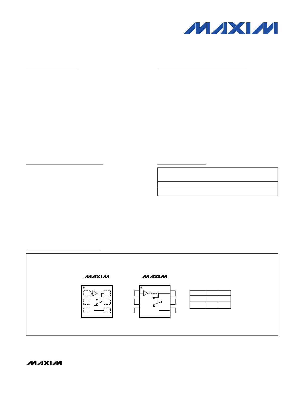
MAX4714
0.8Ω, Low-Voltage, Single-Supply
SPDT Analog Switch in SC70
________________________________________________________________ Maxim Integrated Products 1
TOP VIEW
6
5
4
1
2
3
NO
COM
NC
GND
V+
IN
MAX4714
SC70-6
LOGIC NC
0
1
ON
OFF
NO
OFF
ON
SWITCHES SHOWN
FOR LOGIC 0 INPUT
6
5
4
1
2
3
NO
COM
NC
GND
V+
IN
MAX4714
µDFN
19-1982; Rev 1; 5/04
Ordering Information
Pin Configurations/Functional Diagrams/Truth Table
PART
TEMP RANGE
PIN-
TOP
MARK
MAX4714EXT-T
6 SC70-6 AAY
MAX4714ELT-T
6 µDFN-6 AJ
PACKAGE
-40°C to +85°C
-40°C to +85°C
Page 2
MAX4714
0.8Ω, Low-Voltage, Single-Supply
SPDT Analog Switch in SC70
2 _______________________________________________________________________________________
ABSOLUTE MAXIMUM RATINGS
Stresses beyond those listed under “Absolute Maximum Ratings” may cause permanent damage to the device. These are stress ratings only, and functional
operation of the device at these or any other conditions beyond those indicated in the operational sections of the specifications is not implied. Exposure to
absolute maximum rating conditions for extended periods may affect device reliability.
Voltages Referenced to GND
V+, IN ....................................................................-0.3V to +4V
COM, NC, NO (Note 1)..............................-0.3V to (V+ + 0.3V)
Continuous Current NO, NC to COM..............................±150mA
Peak Current NO, NC to COM
(pulsed at 1ms, 10% duty cycle max)........................ ±300mA
Continuous Power Dissipation
6-Pin SC70 (derate 3.1mW/°C above +70°C)...............247mW
6-Pin µDFN-6 (derate 2.1mW/°C above +70°C) ...........167mW
Operating Temperature Range
MAX4714EXT....................................................-40°C to +85°C
Junction Temperature......................................................+150°C
Storage Temperature Range .............................-65°C to +150°C
Lead Temperature (soldering, 10s) ................................ +300°C
Note 1: Signals on NC, NO, and COM exceeding V+ or GND are clamped by internal diodes.
ELECTRICAL CHARACTERISTICS—Single +3V Supply
(V+ = +2.7V to +3.6V, VIH= +1.4V, VIL= +0.5V, TA= T
MIN
to T
MAX
, unless otherwise noted. Typical values are at V+ = +3.0V and
T
A
= +25°C.) (Notes 2, 3)
PARAMETER
CONDITIONS T
A
UNITS
ANALOG SWITCH
Analog Signal Range
V
COM
,
0V+V
+25°C 0.6 0.8
On-Resistance (Note 4) R
ON
V+ = 2.7V, I
COM
= 100mA,
V
NO
or VNC = 1.5V
0.9
Ω
+25°C
On-Resistance Match
Between Channels (Note 5)
∆R
ON
V+ = 2.7V, I
COM
= 100mA,
V
NO
or VNC = 1.5V
Ω
+25°C 0.1
On-Resistance Flatness
(Note 6)
)
V+ = 2.7V, I
COM
= 100mA,
V
NO
or VNC = 0.6V, 1.5V, 2.1V
0.2
Ω
+25°C-1 +1
NO or NC Off-Leakage
Current
I
NO(OFF),
)
V+ = 3.3V, V
COM
= 0.3V, 3V,
V
NO
or VNC = 3V, 0.3V
-5 +5
nA
+25°C-2 +2
COM On-Leakage Current
)
V + = 3.3V , V
C OM
= 0.3V , 3V ,
-10
nA
DYNAMIC
+25°C1318
Turn-On Time t
ON
VNO or VNC = 1.5V, RL = 50Ω,
C
L
= 35pF, Figure 1
20
ns
+25°C612
Turn-Off Time t
OFF
VNO or VNC = 1.5V, RL = 50Ω,
C
L
= 35pF, Figure 1
15
ns
+25°C19
Break-Before-Make Delay
(Note 7)
t
BBM
VNO or VNC = 1.5V, RL = 50Ω,
C
L
= 35pF, Figure 2
1
ns
Charge Injection Q
+25°C22pC
Off-Isolation (Note 8) V
ISO
f = 1MHz, V
COM
= 1V
RMS
,
R
L
= 50Ω, CL = 5pF, Figure 4
+25°C -54 dB
Crosstalk (Note 9)
f = 1MHz, V
COM
= 1V
RMS
,
R
L
= 50Ω, CL = 5pF, Figure 4
+25°C -54 dB
Total Harmonic Distortion THD
f = 20H z to 20kH z, V
C OM
= 2V
P - P
,
R
L
= 32Ω
+25°C
%
SYMBOL
VNO, V
NC
MIN TYP MAX
R
FLAT(ON
I
NC(OFF
I
COM(ON
V
N O
V
GE N
or V
N C
, R
GE N
= 0.3V , 3V or fl oati ng
, C
= 1.0nF, Fi g ur e 3
L
T
to T
MIN
MAX
0.03 0.06
T
MIN
to T
MAX
0.08
0.18
T
to T
MIN
MAX
T
to T
MIN
MAX
+10
T
MIN
to T
MAX
0.01
T
to T
MIN
MAX
T
to T
MIN
MAX
T
to T
MIN
MAX
Page 3
MAX4714
0.8Ω, Low-Voltage, Single-Supply
SPDT Analog Switch in SC70
_______________________________________________________________________________________ 3
PARAMETER
CONDITIONS T
A
UNITS
NC or NO Off-Capacitance
C
NO(OFF),
)
f = 1MHz, Figure 5 +25°C30pF
COM On-Capacitance
)
f = 1MHz, Figure 5 +25°C65pF
LOGIC INPUT
Input Voltage Low V
IL
0.5 V
Input Voltage High V
IH
1.4 V
Input Leakage Current I
IN
VIN = 0V or V+ -1 +1 µA
SUPPLY
Power-Supply Range V+ 1.6 3.6 V
+25°C
0.2
Positive Supply Current I+ V+ = +3.6V, VIN = 0V or V+
2
µA
ELECTRICAL CHARACTERISTICS—Single +1.8V Supply
(V+ = +1.8V, VIH= +1V, VIL= +0.4V, TA= T
MIN
to T
MAX
, unless otherwise noted. Typical values are at TA= +25°C.) (Notes 2, 3)
PARAMETER
CONDITIONS T
A
UNITS
ANALOG SWITCH
Analog Signal Range
V
COM
,
0V+V
+25°C 1.2 2.5
On-Resistance R
ON
I
COM
= 10mA,
V
NO
or VNC = +0.9V
5
Ω
+25°C-1
+1
NO or NC Off-Leakage
Current
I
NO(OFF),
)
V
COM
= 0.3V, 1.5V,
V
NO
or VNC = 1.5V, 0.3V
-5 +5
nA
+25°C-2 +2
COM On-Leakage Current
)
V
C OM
= 0.3V , 1.5V , V
N O
or
V
N C
= 0.3V , 1.5V or fl oati ng
-10
nA
DYNAMIC
+25°C1825
Turn-On Time t
ON
VNO or VNC = 1.5V, RL = 50Ω,
C
L
= 35pF, Figure 1
30
ns
+25°C915
Turn-Off Time t
OFF
VNO or VNC = 1.5V, RL = 50Ω,
C
L
= 35pF, Figure 1
18
ns
+25°C2
Break-Before-Make Delay
(Note 7)
t
BBM
VNO or VNC = 1.5V, RL = 50Ω,
C
L
= 35pF, Figure 2
2
ns
Charge Injection Q
V
GE N =
0V, R
GE N =
0, C
L
= 1nF,
Fi g ur e 3
+25°C12pC
ELECTRICAL CHARACTERISTICS—Single +3V Supply (continued)
(V+ = +2.7V to +3.6V, VIH= +1.4V, VIL= +0.5V, TA= T
MIN
to T
MAX
, unless otherwise noted. Typical values are at V+ = +3.0V and
TA= +25°C.) (Notes 2, 3)
SYMBOL
C
NC(OFF
C
COM(ON
T
to T
MIN
MAX
SYMBOL
MIN TYP MAX
0.04
MIN TYP MAX
VNO, V
NC
T
to T
MIN
MAX
0.01
I
NC(OFF
I
COM(ON
T
to T
MIN
MAX
T
to T
MIN
MAX
T
to T
MIN
T
T
MAX
to T
MIN
MAX
MIN
to T
MAX
+10
Page 4

MAX4714
0.8Ω, Low-Voltage, Single-Supply
SPDT Analog Switch in SC70
4 _______________________________________________________________________________________
Note 2: The algebraic convention, where the most negative value is a minimum and the most positive value is a maximum, is used in
this data sheet.
Note 3: Parts are 100% tested at +25°C. Limits across the full temperature range are guaranteed by design and
correlation.
Note 4: Guaranteed by design for µDFN package.
Note 5:
∆RON= R
ON(MAX)
- R
ON(MIN)
.
Note 6: Flatness is defined as the difference between the maximum and minimum values of on-resistance as measured over the
specified analog signal range.
Note 7: Guaranteed by design.
Note 8: Off-Isolation = 20log
10[VCOM
/ (VNCor VNO)], V
COM
= output, VNCor VNO= input to off switch.
Note 9: Between the two switches.
ELECTRICAL CHARACTERISTICS—Single +1.8V Supply (continued)
(V+ = +1.8V, VIH= +1V, VIL= +0.4V, TA= T
MIN
to T
MAX
, unless otherwise noted. Typical values are at TA= +25°C.) (Notes 2, 3)
PARAMETER
SYMBOL
CONDITIONS T
A
MIN
TYP
MAX
UNITS
LOGIC INPUT
Input Voltage Low V
IL
0.4 V
Input Voltage High V
IH
1V
Input Leakage Current I
IN
VIN = 0V or V+ 1 µA
SUPPLY
+25°C
0.2
Positive Supply Current I+ VIN = 0V or V+
2
µA
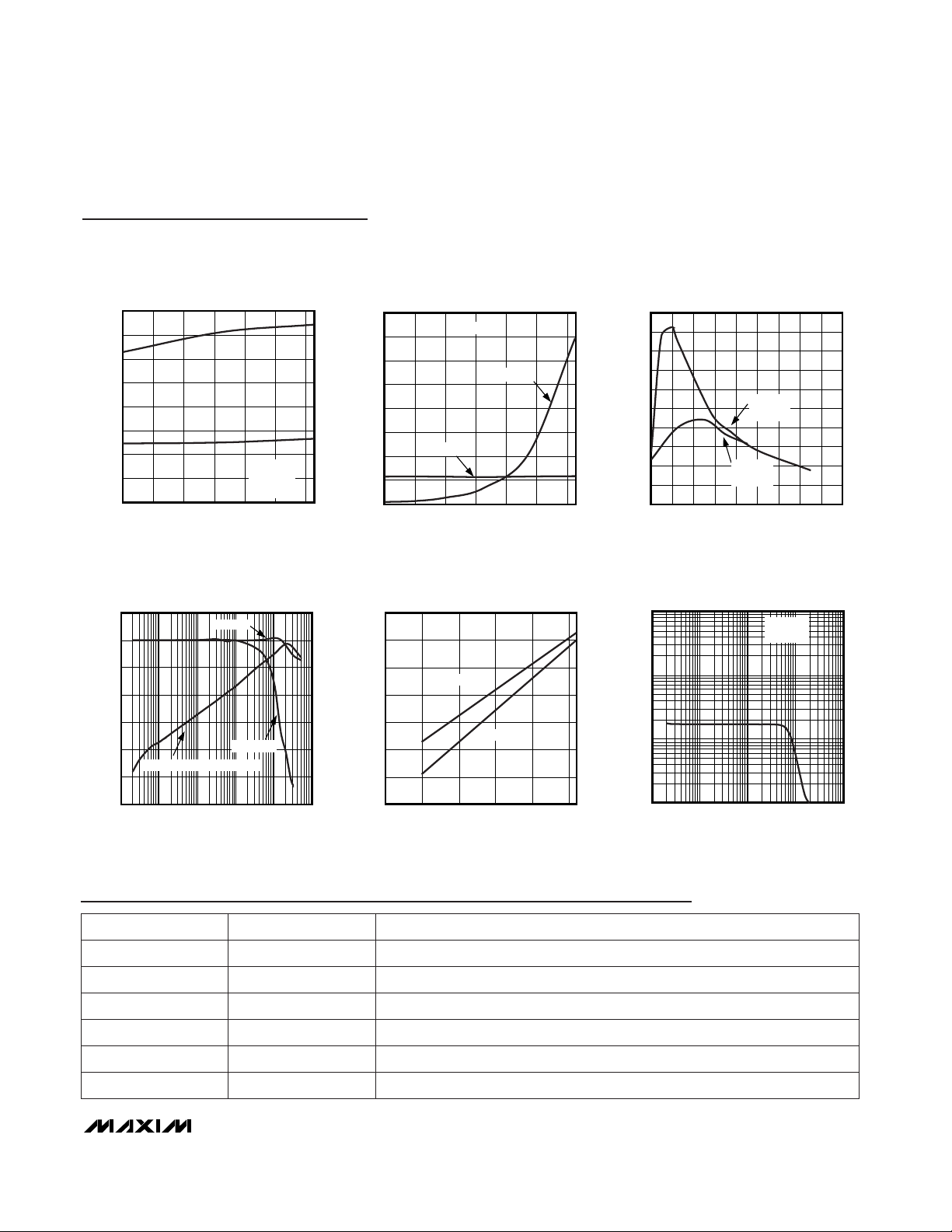
Typical Operating Characteristics
(TA = +25°C, unless otherwise noted.)
0.4
0.6
0.5
0.8
0.7
0.9
1.0
1.1
1.2
0 1.0 1.50.5 2.0 2.5 3.0 3.5
ON-RESISTANCE
vs. COM VOLTAGE OVER SUPPLY VOLTAGE
MAX4714 toc01
V
COM
(V)
R
ON
(Ω)
V+ = +1.8V
V+ = +2.0V
V+ = +2.5V
V+ = +2.7V
V+ = +3.0V
V+ = +3.6V
I
COM
= 100mA
V+ = +3.3V
0.30
0.40
0.35
0.55
0.50
0.45
0.70
0.65
0.60
0.75
0 1.00.5 1.5 2.0 2.5
ON-RESISTANCE
vs. COM VOLTAGE OVER TEMPERATURE
MAX4714 toc02
V
COM
(V)
R
ON
(Ω)
V+ = +2.7V
I
COM
= 100mA
TA = +85°C
TA = +65°C
TA = +25°C
TA = 0°C
TA = -20°C
TA = -40°C
0
6
4
2
8
10
12
14
16
18
20
1.0 2.01.5 2.5 3.0 3.5
TURN-ON/OFF TIMES
vs. SUPPLY VOLTAGE
MAX4714 toc03
SUPPLY VOLTAGE (V)
t
ON
/t
OFF
(ns)
t
ON
t
OFF
RL = 50Ω
T
MIN
to T
MAX
0.04
Page 5
MAX4714
0.8Ω, Low-Voltage, Single-Supply
SPDT Analog Switch in SC70
_______________________________________________________________________________________ 5
Typical Operating Characteristics (continued)
(TA = +25°C, unless otherwise noted.)
TURN-ON/OFF TIMES
vs. TEMPERATURE
MAX4714 toc04
0
2
6
4
12
14
10
8
16
t
ON
/t
OFF
(ns)
-40 0 20-20
40
60 80
TEMPERATURE (°C)
t
ON
t
OFF
V+ = +2.7V
R
L
= 50Ω
C
L
= 35pF
ON/OFF-LEAKAGE CURRENT
vs. TEMPERATURE
MAX4714 toc05
0
0.5
1.5
1.0
3.0
3.5
2.5
2.0
4.0
ON/OFF-LEAKAGE CURRENT (nA)
-40 0 20-20
40
60 80
TEMPERATURE (°C)
I
COM(OFF)
I
COM(ON)
V+ = 3.3V
0
10
5
20
15
30
25
35
45
40
50
0 0.8 1.2 1.60.4 2.0 2.4 2.8 3.2 3.6
CHARGE INJECTION vs. COM VOLTAGE
MAX4714 toc06
V
COM
(V)
Q (pC)
V+ = 3V
C
L
= 1nF
V+ = 1.8V
C
L
= 1nF
FREQUENCY RESPONSE
MAX4714 toc07
FREQUENCY (Hz)
LOSS (dB)
20
-120
-100
-40
-20
0
10k 10M 100M100k 1M 1G
-60
-80
OFF-ISOLATION/CROSSTALK
ON-PHASE
ON-LOSS
0.4
0.6
0.5
0.8
0.7
1.0
0.9
1.1
1.0 2.0 2.51.5 3.0 3.5
LOGIC THRESHOLD VOLTAGE
vs. SUPPLY VOLTAGE
MAX4714 toc08
SUPPLY VOLTAGE (V)
LOGIG THRESHOLD VOLTAGE (V)
VIN RISING
VIN FALLING
10 1k 100k
TOTAL HARMONIC DISTORTION
vs. FREQUENCY
MAX4714 toc09
FREQUENCY (Hz)
THD (%)
1
0.1
0.001
0.01
100 10k
RL = 32Ω
V+ = 3V
Pin Description
Analog Switch—CommonCOM5
Analog Switch—Normally OpenNO6
Analog Switch—Normally ClosedNC4
GroundGND3
PIN
Positive Supply Voltage InputV+2
Digital Control InputIN
1
FUNCTIONNAME
Page 6

MAX4714
0.8Ω, Low-Voltage, Single-Supply
SPDT Analog Switch in SC70
6 _______________________________________________________________________________________
tr < 5ns
tf < 5ns
50%
V
INL
LOGIC
INPUT
R
L
50Ω
COM
GND
IN
C
L
INCLUDES FIXTURE AND STRAY CAPACITANCE.
V
OUT
= V
N_ (
R
L
)
RL + R
ON
V
INH
t
OFF
0V
NO
OR NC
0.9 × V
0UT
0.9 × V
OUT
t
ON
V
OUT
SWITCH
OUTPUT
LOGIC
INPUT
LOGIC INPUT WAVEFORMS INVERTED FOR SWITCHES
THAT HAVE THE OPPOSITE LOGIC SENSE.
V+
C
L
35pF
V+
V
OUT
MAX4714
Figure 1. Switching Time
50%
V
INH
V
INL
LOGIC
INPUT
V
OUT
0.9 × V
OUT
t
D
LOGIC
INPUT
R
L
50Ω
GND
C
L
INCLUDES FIXTURE AND STRAY CAPACITANCE.
NO
IN
NC
V
OUT
V+
V+
C
L
35pF
V
N_
COM
MAX4714
Figure 2. Break-Before-Make Interval
Test Circuits/Timing Diagrams
Detailed Description
The MAX4714 is a low-on-resistance (RON), low-voltage, single-pole/double-throw (SPDT) analog switch
that operates from a +1.6V to +3.6V supply. The
MAX4714 has break-before-make switching. This
device also has fast switching speeds (tON= 18ns,
max, t
OFF
= 12ns, max).
When powered from a +3V supply, the 0.8Ω (max) R
ON
allows high continuous currents to be switched in a
variety of applications.
Applications Information
Logic Inputs
The MAX4714 logic input can be driven up to +3.6V
regardless of the supply voltage. For example, with a
+3.3V supply, IN may be driven low to GND and high to
+3.6V. Driving IN rail-to-rail minimizes power consumption.
Analog Signal Levels
Analog signals that range over the entire supply voltage
(V+ to GND) can be passed with very little change in
on-resistance (see Typical Operating Characteristics).
The switches are bidirectional, so the NO, NC, and
COM pins can be used as either inputs or outputs.
Chip Information
TRANSISTOR COUNT: 135
PROCESS: CMOS
Page 7

MAX4714
0.8Ω, Low-Voltage, Single-Supply
SPDT Analog Switch in SC70
_______________________________________________________________________________________ 7
CAPACITANCE
METER
NC or
NO
COM
GND
IN
V
INL
OR
V
INH
10nF
V+
f = 1MHz
V+
MAX4714
Figure 5. Channel Off/On-Capacitance
V
GEN
GND
COM
C
L
V
OUT
V+
V
OUT
IN
OFF
ON
OFF
∆V
OUT
Q = (∆V
OUT
)(CL)
NC
OR NO
IN DEPENDS ON SWITCH CONFIGURATION;
INPUT POLARITY DETERMINED BY SENSE OF SWITCH.
OFF
ON
OFF
IN
V
INL
TO V
INH
V+
R
GEN
IN
MAX4714
Figure 3. Charge Injection
MEASUREMENTS ARE STANDARDIZED AGAINST SHORTS AT IC TERMINALS.
OFF-ISOLATION IS MEASURED BETWEEN COM_ AND "OFF" NO_ OR NC_ TERMINAL ON EACH SWITCH.
ON-LOSS IS MEASURED BETWEEN COM_ AND "ON" NO_ OR NC_TERMINAL ON EACH SWITCH.
CROSSTALK IS MEASURED FROM ONE CHANNEL TO ALL OTHER CHANNELS.
SIGNAL DIRECTION THROUGH SWITCH IS REVERSED; WORST VALUES ARE RECORDED.
+3V
V
OUT
V+
IN
NC
COM
NO
V
IN
MAX4714
OFF-ISOLATION = 20log
V
OUT
V
IN
ON-LOSS = 20log
V
OUT
V
IN
CROSSTALK = 20log
V
OUT
V
IN
NETWORK
ANALYZER
50Ω
50Ω 50Ω
50Ω
MEAS REF
10nF
0 OR V+
50Ω
GND
Figure 4. On-Loss, Off-Isolation, and Crosstalk
Test Circuits/Timing Diagrams (continued)
Page 8
SC70, 6L.EPS
PACKAGE OUTLINE, 6L SC70
21-0077
1
1
C
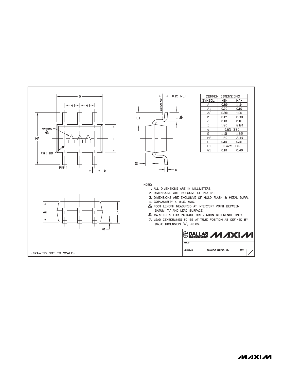
Package Information
(The package drawing(s) in this data sheet may not reflect the most current specifications. For the latest package outline information
go to www.maxim-ic.com/packages
.)
MAX4714
0.8Ω, Low-Voltage, Single-Supply
SPDT Analog Switch in SC70
8 _______________________________________________________________________________________
Page 9

Maxim cannot assume responsibility for use of any circuitry other than circuitry entirely embodied in a Maxim product. No circuit patent licenses are
implied. Maxim reserves the right to change the circuitry and specifications without notice at any time.
Maxim Integrated Products, 120 San Gabriel Drive, Sunnyvale, CA 94086 408-737-7600 _____________________ 9
© 2004 Maxim Integrated Products Printed USA is a registered trademark of Maxim Integrated Products.
MAX4714
0.8Ω, Low-Voltage, Single-Supply
SPDT Analog Switch in SC70
Package Information (continued)
(The package drawing(s) in this data sheet may not reflect the most current specifications. For the latest package outline information
go to www.maxim-ic.com/packages
.)
6L UDFN.EPS
L
TOP VIEW
D
E
SIDE VIEW
A1
PIN 1
INDEX AREA
A
A 0.64
COMMON DIMENSIONS
PIN 1
0.075x45¡
BOTTOM VIEW
L1
32
MIN.
1
e
6
5
b
4
SECTION A-A
b
L2
A A
NOM.
0.72 0.80
MAX.
0.20--A1 --
1.501.45D 1.55
1.000.95E 1.05
0.350.30L 0.40
----L1 0.08
----L2 0.05
0.200.17b 0.23
0.50 BSC.e
AAA
TOPMARK
2
1
-DRAWING NOT TO SCALE-
DOCUMENT CONTROL NO.APPROVAL
TITLE:
REV.
PACKAGE OUTLINE, 6L uDFN, 1.5x1.0x0.8mm
21-0147
1
1
C
3
 Loading...