

General Description
The MAX4704 low-voltage, 4-channel analog multiplexer operates from a single +1.8V to +5.5V supply. The
MAX4704 features break-before-make switching action
with a t
ON
= 60ns and t
OFF
= 20ns at +3V.
When powered from a +2.7V supply, the device has a
60Ω (max) on-resistance (R
ON
), with 3Ω (max) R
ON
matching and 5Ω max RONflatness. The digital logic
inputs are 1.8V-logic compatible from a +2.7V to +3.3V
supply. The MAX4704 is available in both a space-saving 12-pin QFN (3mm x 3mm) package and a 10-pin
µMAX package.
Applications
MP3 Players
Battery-Operated Equipment
Relay Replacement
Audio and Video Signal Routing
Low-Voltage Data-Acquisition Systems
Communications Circuits
PCMCIA Cards
Cellular Phones
Modems
Features
♦ 3mm x 3mm 12-Pin QFN Package
♦ Guaranteed On-Resistance:
60Ω (max) (+2.7V Supply)
40Ω (max) (+5V Supply)
♦ Guaranteed Match Between Channels: 3Ω (max)
♦ Guaranteed Flatness Over Signal Range:
5Ω (max)
♦ Guaranteed Low Leakage Currents:
100pA (max) at +25°C
♦ Switching Time: t
ON
= 60ns, t
OFF
= 20ns
♦ +1.8V to +5.5V Single-Supply Operation
♦ Rail-to-Rail Signal Handling
♦ -3dB Bandwidth: >200MHz
♦ Low Crosstalk: -90dB (1MHz)
♦ High Off-Isolation: -85dB (1MHz)
♦ Low 3pC Charge Injection
♦ THD: 0.02%
♦ +1.8V CMOS-Logic Compatible
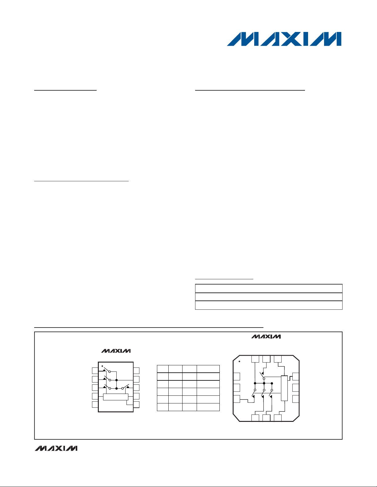
MAX4704
Low-Voltage, 60Ω,
4:1 Analog Multiplexer in QFN
________________________________________________________________
Maxim Integrated Products
1
1
2
3
4
5
10
9
8
7
6
V+
COM
NO0
ADDAINH
NO1
NO3
NO2
MAX4704
μMAX
TOP VIEW
ADDBGND
X = DON’T CARE
N.C. = NO CONNECT
LOGIC
MAX4704
INH
1
0
0
0
0
ADDB
X
0
0
1
1
ADDA
X
0
1
0
1
ON SWITCH
NONE
COM-NO0
COM-NO1
COM-NO2
COM-NO3
12
COM11NO010ADDA
9 ADDB
8 N.C.
7 GND
4
NO35NO16INH
1V+
2N.C.
3NO2
LOGIC
QFN
Pin Configurations
Ordering Information
19-2240; Rev 1; 10/08
PART TEMP. RANGE PIN-PACKAGE
MAX4704EGC
-40°C to +85°C 12 QFN-EP*
MAX4704EUB -40°C to +85°C 10 µMAX
For pricing, delivery, and ordering information, please contact Maxim/Dallas Direct! at
1-888-629-4642, or visit Maxim’s website at www.maxim-ic.com.
*
EP = Exposed Pad
MAX4704
Low-Voltage, 60Ω,
4:1 Analog Multiplexer in QFN
2 _______________________________________________________________________________________
ABSOLUTE MAXIMUM RATINGS
ELECTRICAL CHARACTERISTICS—Single +3V Supply
(V+ = +2.7V to +3.3V, VIH= +1.4V, VIL= +0.5V, TA= -40°C to +85°C, unless otherwise noted. Typical values are at V+ = +3V and
T
A
= +25°C.) (Notes 2, 3)
Stresses beyond those listed under “Absolute Maximum Ratings” may cause permanent damage to the device. These are stress ratings only, and functional
operation of the device at these or any other conditions beyond those indicated in the operational sections of the specifications is not implied. Exposure to
absolute maximum rating conditions for extended periods may affect device reliability.
Note 1: Signals on INH, ADD_, NO_, and COM exceeding V+ or GND are clamped by internal diodes. Limit forward-diode current to
maximum current rating.
(Voltages Referenced to GND)
V+ .............................................................................-0.3V to +6V
All Other Pins (Note 1)................................ -0.3V to (V+ + 0.3V)
Continuous Current COM, NO_ ........................................±20mA
Peak Current COM, NO_
(pulsed at 1ms, 10% duty cycle)..................................±40mA
ESD per Method 3015.7.......................................................>2kV
Continuous Power Dissipation (T
A
= +70°C)
10-Pin µMAX (derate 4.7mW/°C above +70°C) ......... 330mW
12-Pin QFN (derate 11.9mW/°C above +70°C) ......... 952mW
Operating Temperature Range .......................... -40°C to +85°C
Storage Temperature Range ............................ -65°C to +150°C
Lead Temperature (soldering, 10s) ................................ +300°C
PARAMETER
CONDITIONS T
A
ANALOG SWITCH
Analog Signal Range
0
V
+25°C5060
On-Resistance R
ON
V+ = +2.7V, I
COM
= 5mA,
V
NO_
= +1.3V
70
Ω
+25°C13
On-Resistance Match
Between Channels (Note 4)
ΔR
ON
V+ = +2.7V, I
COM
= 5mA,
V
NO_
= +1.3V
5
Ω
+25°C35
On-Resistance Flatness
(Note 5)
)
V+ = +2.7V, I
COM
= 5mA,
V
NO_
= +1V, +1.3V, +1.8V
10
Ω
+25°C
NO_ Off-Leakage
Current (Note 6)
V+ = +3.3V, V
COM
= +0.3V, +3V
V
NO_
= +3V, +0.3V
1
nA
+25°C
COM On-Leakage Current
(Note 6)
V + = + 3.3V , V
C OM
= + 0.3V , +3V
V
N O_
= + 0.3V , + 3V , or fl oati ng
5
nA
+25°C
COM Off-Leakage Current
(Note 6)
V+ = +3.3V, V
COM
= +0.3V, +3V
V
NO_
= +3V, +0.3V
5
nA
DYNAMIC
+25°C2060
Address Transition Time t
TRANS
V
N O_
= +1.5V, RL = 300Ω,
C
L
= 35pF, Figure 2
70
ns
+25°C2560
Inhibit Turn-On Time t
ON
V
N O
_ = +1.5V, RL = 300Ω,
C
L
= 35pF, Figure 3
70
ns
+25°C1020
Inhibit Turn-Off Time t
OFF
V
N O
_ = +1.5V, RL = 300Ω,
C
L
= 35pF, Figure 3
30
ns
+25°C20
Break-Before-Make Time
(Note 7)
t
BBM
V
N O
_ = +1.5V, RL = 300Ω,
C
L
= 35pF, Figure 4
2
ns
Charge Injection Q
V
GEN
= 0, R
GEN
= 0, CL = 1.0nF,
Figure 5
2pC
SYMBOL
V
, V
COM
NO_
MIN TYP MAX UNITS
V+
R
FLAT (ON
I
N O_ ( OFF )
I
C OM ( ON )
I
C OM ( OFF )
T
to T
MIN
MAX
T
to T
MIN
MIN
MIN
MIN
MIN
MIN
to T
to T
to T
to T
to T
MAX
MAX
-0.1 ±0.01 0.1
-1
MAX
MAX
-0.5 ±0.01 0.5
-5
-0.5 ±0.01 0.5
-5
MAX
MAX
T
T
T
T
T
T
to T
MIN
MIN
MIN
to T
to T
MAX
MAX
MAX
T
T
MAX4704
Low-Voltage, 60Ω,
4:1 Analog Multiplexer in QFN
_______________________________________________________________________________________ 3
ELECTRICAL CHARACTERISTICS—Single +5V Supply
(V+ = +4.5V to +5.5V, VIH= +2.0V, VIL= +0.8V, TA= -40°C to +85°C, unless otherwise noted. Typical values are at V+ = +5V and
T
A
= +25°C.) (Notes 2, 3)
PARAMETER
CONDITIONS T
A
ANALOG SWITCH
Analog Signal Range
0
V
+25°C3040
On-Resistance R
ON
V+ = +4.5V, I
COM
= 5mA,
V
NO_
= +3.5V
50
Ω
+25°C12
On-Resistance Match
Between Channels (Note 4)
ΔR
ON
V+ = +4.5V, I
COM
= 5mA,
V
NO_
= +3.5V
3
Ω
+25°C35
On-Resistance Flatness
(Note 5)
)
V+ = +4.5V, I
COM
= 5mA,
V
NO_
= +1V, +2.25V, +3.5V
10
Ω
+25°C
NO_ Off-Leakage
Current (Note 6)
V+ = +5.5V, V
COM
= +0.5V, +5V
V
NO_
= +5V, +0.5V
1
nA
+25°C
COM On-Leakage Current
(Note 6)
V + = + 5.5V , V
C OM
= + 0.5V , +5V
V
N O_
= + 0.5V , +5V , or fl oati ng
5
nA
ELECTRICAL CHARACTERISTICS—Single +3V Supply (continued)
(V+ = +2.7V to +3.3V, VIH= +1.4V, VIL= +0.5V, TA= -40°C to +85°C, unless otherwise noted. Typical values are at V+ = +3V and
T
A
= +25°C.) (Notes 2, 3)
PARAMETER
SYMBOL
CONDITIONS T
A
MIN
TYP
MAX
UNITS
BW
Signal = 0dBm, 50Ω in and out,
Figure 6
Off-Isolation (Note 8) V
ISO
f = 1MHz, R
L
= 50Ω, C
L
= 5pF,
Figure 6
dB
Crosstalk (Note 9) V
CT
f = 1MHz, R
L
= 50Ω, CL = 5pF,
Figure 6
dB
NO_ Off-Capacitance
f = 1MHz, V
N O
_ = GND, Figure 7 7 pF
COM On-Capacitance
)
f = 1MHz, V
N O
_ = GND, Figure 7 19 pF
COM Off-Capacitance
)
f = 1MHz, V
N O
_ = GND, Figure 7 15 pF
DIGITAL I/O
Input Logic High V
IH
V
Input Logic Low V
IL
V
Input Leakage Current IIH, I
IL
ADD_, INH = 0 or V+
1µA
SUPPLY
Power-Supply Range V+
V
Power-Supply Current I+ V+ = +5.5V, ADD_, INH = 0 or V+ 1 µA
On-Channel -3dB Bandwidth
C
N O_ ( OFF)
C
COM(ON
C
COM(OFF
>200 MHz
-85
-90
1.4
0.5
-1
1.8 5.5
SYMBOL
V
, V
COM
NO_
R
FLAT (ON
I
N O_ ( OFF )
I
C OM ( ON )
MIN TYP MAX UNITS
T
T
T
T
T
MIN
MIN
MIN
MIN
MIN
to T
to T
to T
to T
to T
MAX
MAX
MAX
-0.1 ±0.01 0.1
-1
MAX
-0.5 ±0.01 0.5
-5
MAX
V+
MAX4704
Low-Voltage, 60Ω,
4:1 Analog Multiplexer in QFN
4 _______________________________________________________________________________________
Note 2: The algebraic convention, where the most negative value is a minimum and the most positive value a maximum, is used in
this data sheet.
Note 3: -40°C specifications are guaranteed by design.
Note 4: ΔR
ON
= R
ON(MAX)
- R
ON(MIN)
.
Note 5: Flatness is defined as the difference between the maximum and minimum value of on-resistance as measured over the
specified analog signal ranges.
Note 6: Leakage currents are 100% tested at T
A
= +85°C. Limits across the full temperature range are guaranteed by correlation.
Note 7: Guaranteed by design.
Note 8: Off-Isolation = 20log10(V
COM
/ V
NO_
), V
COM
= output, V
NO_
= input to off switch.
Note 9: Between any two switches.
ELECTRICAL CHARACTERISTICS—Single +5V Supply (continued)
(V+ = +4.5V to +5.5V, VIH= +2.0V, VIL= +0.8V, TA= -40°C to +85°C, unless otherwise noted. Typical values are at V+ = +5V and
T
A
= +25°C.) (Notes 2, 3)
PARAMETER
CONDITIONS T
A
+25°C
COM Off-Leakage Current
V+ = +5.5V, V
COM_
= +0.5V, +5V
V
NO_
= +5V, +0.5V
5
nA
DYNAMIC
+25°C1535
Address Transition Time t
TRANS
V
N O_
= +3V, RL = 300Ω,
C
L
= 35pF, Figure 2
40
ns
+25°C1835
Inhibit Turn-On Time t
ON
V
N O_
= +3V, RL = 300Ω,
C
L
= 35pF, Figure 3
40
ns
+25°C920
Inhibit Turn-Off Time t
OFF
V
N O_
= +3V, RL = 300Ω,
C
L
= 35pF, Figure 3
30
ns
+25°C20
Break-Before-Make Time
(Note 7)
t
BBM
V
N O_
= +3V, RL = 300Ω,
C
L
= 35pF, Figure 4
2
ns
Charge Injection Q
V
GEN
= 0, R
GEN
= 0, CL = 1.0nF,
Figure 5
3pC
BW
Signal = 0dBm, 50Ω in and out,
Figure 6
Off-Isolation (Note 8) V
ISO
f = 1MHz, R
L
= 50Ω, C
L
= 5pF,
Figure 6
dB
Crosstalk (Note 9) V
CT
f = 1MHz, R
L
= 50Ω, C
L
= 5pF,
Figure 6
dB
Total Harmonic Distortion THD
%
DIGITAL I/O
Input Logic High V
IH
V
Input Logic Low V
IL
V
Input Leakage Current IIH, I
IL
ADD_, INH = 0 or V+
1µA
SUPPLY
Power-Supply Range V+
V
Positive Supply Current I+ V+ = +5.5V, ADD_, INH = 0 or V+ 1 µA
SYMBOL
I
C OM ( OFF )
T
MIN
to T
MIN TYP MAX UNITS
-0.5 ±0.01 0.5
-5
MAX
T
to T
MIN
MAX
T
to T
MIN
MAX
T
to T
MIN
MAX
T
to T
MIN
MAX
On-Channel -3dB Bandwidth
f = 20Hz to 20kHz, 1Vp-p, RL = 600Ω 0.02
>200 MHz
-85
-90
2.0
-1
1.8 5.5
0.8

MAX4704
Low-Voltage, 60Ω,
4:1 Analog Multiplexer in QFN
_______________________________________________________________________________________ 5
0
20
10
50
40
30
80
70
60
90
021 345
ON-RESISTANCE VS. V
COM
MAX4704 toc01
V
COM
(V)
R
ON
(Ω)
V+ = 2.5V
V+ = 1.8V
V+ = 5.0V
V+ = 3.0V
0
5
10
15
20
25
30
35
40
01.00.5 1.5 2.0 2.5 3.0
ON-RESISTANCE VS. V
COM
(V+ = 3V)
MAX4704 toc02
V
COM
(V)
R
ON
(Ω)
TA = +25°C
T
A
= +85°C
T
A
= -40°C
0
5
15
10
20
25
021345
ON-RESISTANCE VS. V
COM
(V+ = 5V)
MAX4704 toc03
V
COM
(V)
R
ON
(Ω)
TA = +25°C
TA = +85°C
TA = -40°C
Typical Operating Characteristics
(TA = +25°C, unless otherwise noted.)
0
3
9
6
12
15
-40 10-15 35 60 85
SUPPLY CURRENT VS. TEMPERATURE
MAX4704 toc04
TEMPERATURE (°C)
SUPPLY CURRENT (nA)
V+ = +5V
V
INH
= 0
V+ = +3V
1000
100
10
1
0.1
021 345
SUPPLY CURRENT VS.
LOGIC INPUT VOLTAGE
MAX4704 toc05
ADDA (V)
SUPPLY CURRENT (μA)
V+ = +5V
V
ADDB
= 0
V+ = +3V
COM ON-LEAKAGE CURRENT
vs. TEMPERATURE
MAX4704 toc06
TEMPERATURE (°C)
COM ON-LEAKAGE (pA)
603510-15
10
100
1000
1
-40 85
V+ = 5V
V+ = 3V
COM OFF-LEAKAGE CURRENT
vs. TEMPERATURE
MAX4704 toc07
TEMPERATURE (°C)
COM OFF-LEAKAGE (pA)
603510-15
10
100
1000
1
-40 85
COM OFF, V+ = 5V
COM OFF, V+ = 3V
NO_ OFF, V+ = 5V
NO_ OFF, V+ = 3V
0
0.50
0.25
1.00
0.75
1.25
1.50
05
LOGIC THRESHOLD
VS.
SUPPLY VOLTAGE
MAX4704 toc08
V+ (V)
LOGIC THRESHOLD ADD_ (V)
2134
V
IH
V
IL
INHIBIT TURN-ON/OFF TIME
vs. SUPPLY VOLTAGE
MAX4704 toc09
SUPPLY VOLTAGE (V)
INHIBIT TIME (ns)
432
10
15
20
25
30
35
5
15
t
ON
t
OFF

MAX4704
Low-Voltage, 60Ω,
4:1 Analog Multiplexer in QFN
6 _______________________________________________________________________________________
INHIBIT TURN-ON/OFF TIME
vs. TEMPERATURE
MAX4704 toc10
TEMPERATURE (°C)
INHIBIT TIME (ns)
603510-15
5
10
15
20
25
0
-40 85
t
ON
, V+ = 3V
tON, V+ = 5V
t
OFF
, V+ = 3V
t
OFF
, V+ = 5V
CHARGE INJECTION vs. V
COM
MAX4704 toc11
V
COM
(V)
Q (pC)
4321
1
2
3
4
5
6
7
8
9
10
0
05
V+ = 5V
V+ = 3V
FREQUENCY RESPONSE
MAX4704 toc12
FREQUENCY (MHz)
LOSS (dB)
1001010.1
-110
-100
-90
-80
-70
-60
-50
-40
-30
-20
-10
0
-120
0.01 1000
ON-RESPONSE
OFF-ISOLATION
CROSSTALK
Typical Operating Characteristics (continued)
(TA = +25°C, unless otherwise noted.)
ADDRESS TRANSITION TIME
vs. SUPPLY VOLTAGE
MAX4704 toc14
SUPPLY VOLTAGE (V)
ADDRESS TRANSITION TIME (ns)
432
5
10
15
20
25
30
0
15
t
LH
t
HL
THD vs. FREQUENCY
MAX4704 toc13
FREQUENCY (Hz)
THD (%)
10k1k100
0.02
0.03
0.04
0.01
10 100k
V+ = 5V
Vp-p = 1V
R
IN
= R
OUT
= 600Ω
ADDRESS TRANSITION TIME
vs. TEMPERATURE
MAX4704 toc15
TEMPERATURE (°C)
ADDRESS TRANSITION TIME (ns)
603510-15
5
10
15
20
25
0
-40 85
tLH, V+ = 3V
tLH, V+ = 5V
tHL, V+ = 3V
tHL, V+ = 5V

MAX4704
Low-Voltage, 60Ω,
4:1 Analog Multiplexer in QFN
_______________________________________________________________________________________ 7
Detailed Description
The MAX4704 low-voltage, 4-channel analog multiplexer
operates from a single +1.8V to +5.5V supply. When
powered from a +2.7V supply, the device has a 60Ω
(max) on-resistance (RON), with 3Ω (max) RONmatching
and 5Ω (max) RONflatness. The digital logic inputs are
+1.8V-logic compatible from a +2.7V to +3.3V supply.
Applications Information
Digital Control Inputs
The MAX4704 logic inputs are +1.8V CMOS logic compatible for 3V operation and TTL compatible for 5V operation of
V+. Driving ADD_ rail-to-rail minimizes power consumption.
Analog Signal Levels
Analog signals that range over the entire supply voltage (V+ to GND) are passed with very little change in
on-resistance (see
Typical Operating Characteristics
).
The switches are bidirectional, so the NO_ and COM
pins can be either inputs or outputs.
Power-Supply Sequencing and
Overvoltage Protection
Caution: Do not exceed the absolute maximum ratings because stresses beyond those listed may
cause permanent damage to devices.
Proper power-supply sequencing is recommended for all
CMOS devices. Always apply V+ before applying analog
signals, especially if the analog signal is not current limited.
If this sequencing is not possible, and if the analog inputs
are not current limited to <20mA, add a small-signal diode
(D1) as shown in Figure 1. If the analog signal can dip
below GND, add D2. Adding protection diodes reduces
the analog range to a diode drop (about 0.7V) below V+
(for D1), and a diode drop above ground (for D2).
On-resistance increases slightly at low supply voltages.
Maximum supply voltage (V+) must not exceed +6V.
Adding protection diode D2 causes the logic threshold
to be shifted relative to GND. TTL compatibility is not
guaranteed when D2 is added.
Protection diodes D1 and D2 also protect against some
overvoltage situations. In the circuit in Figure 1, if the
supply voltage is below the absolute maximum rating,
and if a fault voltage up to the absolute maximum rating
is applied to an analog signal pin, no damage will result.
POSITIVE SUPPLY
COM
NO
D2
D1
GND
V
g
V+
MAX4704
Figure 1. Overvoltage Protection Using Two External Blocking
Diodes
Pin Description
PIN
µMAX QFN-EP
NAME FUNCTION
10 1 V+ Positive Supply Voltage
— 2, 8 N.C. No Connection. Not internally connected.
1 3 NO2 Analog Switch 2. Normally open.
2 4 NO3 Analog Switch 3. Normally open.
3 5 NO1 Analog Switch 1. Normally open.
46INH
Inhibit. Connect to GND for normal operation. Connect to logic-level high to turn all
switches off.
5 7 GND Ground
6 9 ADDB Address Decoder Selection B
7 10 ADDA Address Decoder Selection A
8 11 NO0 Analog Switch 0. Normally open.
9 12 COM Analog Switch Common Terminal
——EP
Exposed Pad. Internally connected to GND. Connect to a large ground plane to maximize
thermal performance; not intended as an electrical connection point (QFN package only).

MAX4704
Low-Voltage, 60Ω,
4:1 Analog Multiplexer in QFN
8 _______________________________________________________________________________________
Test Circuits/Timing Diagrams
50%
V+
0
V
COM
V
OUT
V
ADD
0
90%
t
BBM
V+
V
OUT
V
ADD
GND
V+
ADDB
ADDA
INH
NO0–N03
COM
V
NO_
MAX4704
300Ω
35pF
tR < 5ns
t
F
< 5ns
Figure 4. Break-Before-Make Interval
50%
t
ON
V+
0
V
NO0
V
OUT
V
INH
0
90%
90%
t
OFF
V
INH
V+
V
OUT
GND
V+
ADDB
ADDA
INH
NO0
NO1–NO3
COM
V
NO_
MAX4704
300Ω
35pF
Figure 3. Inhibit Switching Times
50%
t
TRANS
V+
0
V
NO0
V
OUT
V
ADD
0
90%
90%
t
TRANS
V
ADD
V+
V
OUT
GND
V+
ADDB
ADDA
INH
NO0
NO1–NO2
NO3
COM
V
NO_
MAX4704
300Ω
35pF
Figure 2. Address Transition Time

MAX4704
Low-Voltage, 60Ω,
4:1 Analog Multiplexer in QFN
_______________________________________________________________________________________ 9
Test Circuits/Timing Diagrams (continued)
0
V+
V
INH
Δ V
OUT
IS THE MEASURED VOLTAGE DUE TO CHARGE-
TRANSFER ERROR Q WHEN THE CHANNEL TURNS OFF.
Δ V
OUT
REPEAT TEST FOR EACH SECTION.
Q = Δ V
OUT
X C
L
V
OUT
V+
V
OUT
VNO = 0
V
INH
GND
V+
ADDB
CHANNEL
SELECT
ADDA
INH
NO_
COM
MAX4704
CL
1000pF
Figure 5. Charge Injection
MEASUREMENTS ARE STANDARDIZED AGAINST SHORT AT SOCKET TERMINALS.
OFF-ISOLATION IS MEASURED BETWEEN COM AND "OFF" NO TERMINAL ON EACH SWITCH.
ON-LOSS IS MEASURED BETWEEN COM AND "ON" NO TERMINAL ON EACH SWITCH.
CROSSTALK IS MEASURED FROM ONE CHANNEL (A, B) TO OTHER CHANNEL.
SIGNAL DIRECTION THROUGH SWITCH IS REVERSED; WORST VALUES ARE RECORDED.
V+
V
OUT
V
IN
GND
V+
V
IN
V
OUT
MEAS.
NETWORK
ANALYZER
50Ω 50Ω
50Ω
OFF-ISOLATION = 20log
ON-LOSS = 20log
CROSSTALK = 20log
50Ω
REF.
ADDB
V
OUT
V
IN
V
OUT
V
IN
ADDA
CHANNEL
SELECT
INH
NO_
COM
10nF
MAX4704
Figure 6. Off-Isolation, On-Loss, and Crosstalk
V+
GND
V+
ADDB
ADDA
CHANNEL
SELECT
1MHz
CAPACITANCE
ANALYZER
INH
NO_
NO_
COM
MAX4704
Figure 7. NO_/COM Capacitance
Chip Information
TRANSISTOR COUNT: 256
PROCESS: CMOS

MAX4704
Low-Voltage, 60Ω,
4:1 Analog Multiplexer in QFN
10 ______________________________________________________________________________________
Package Information
For the latest package outline information and land patterns, go to www.maxim-ic.com/packages.
PACKAGE TYPE PACKAGE CODE DOCUMENT NO.
12 QFN-EP G1233-1
21-0102
10 µMAX —
21-0061

MAX4704
Low-Voltage, 60Ω,
4:1 Analog Multiplexer in QFN
Maxim cannot assume responsibility for use of any circuitry other than circuitry entirely embodied in a Maxim product. No circuit patent licenses are
implied. Maxim reserves the right to change the circuitry and specifications without notice at any time.
Maxim Integrated Products, 120 San Gabriel Drive, Sunnyvale, CA 94086 408-737-7600 ____________________
11
© 2008 Maxim Integrated Products Printed USA is a registered trademark of Maxim Integrated Products.
Revision History
REVISION
NUMBER
REVISION
DATE
DESCRIPTION
PAGES
CHANGED
0 10/01 Initial release
⎯
1 10/08 Inserted exposed paddle description 1, 7
 Loading...