

General Description
The MAX4699/MAX4701/MAX4702 are low-voltage,
single-supply CMOS analog switches. The MAX4699/
MAX4701 are dual double-pole/double-throw (DPDT)
switches with two control inputs that control two
single-pole/double-throw (SPDT) switches each. The
MAX4702 is a quad SPDT switch with one control input
and one low-voltage digital logic power supply.
These devices operate from a single +1.8V to +5.5V
power supply. When powered from a +2.7V supply the
MAX4699/MAX4701/MAX4702 offer a 75Ω on-resistance (RON), with 12Ω max RONflatness and 4Ω max
matching between channels. Each switch has rail-to-rail
signal handling, fast switching speeds of t
ON
= 35ns,
t
OFF
= 20ns, and a maximum 1nA of leakage current.
The MAX4699/MAX4701 digital inputs are 1.8V-logic
compatible when operated from a +3V supply. The
MAX4702’s digital inputs feature a 1.0V threshold when
powered with a 1.5V logic supply.
The MAX4699 is available in a space-saving 16-lead
4mm x 4mm TQFN package. The MAX4701/MAX4702
are available in space-saving 16-lead 3mm x 3mm TQFN
16-pin TSSOP packages.
Applications
Audio and Video Signal Routing
Cellular Phones
Battery-Operated Equipment
Communications Circuits
Modems
Features
o 3mm x 3mm and 4mm x 4mm 16-Pin TQFN
Packages
o Guaranteed On-Resistance:
75Ω (max) (+3V Supply)
40Ω (max) (+5V Supply)
o Guaranteed Match Between Channels:
4Ω max
o Guaranteed Flatness Over Signal Range:
12Ω max
o Low Leakage Currents Over Temperature:
1nA Max at +85°C
o Fast Switching: t
ON
= 35ns, t
OFF
= 20ns
o Guaranteed Break-Before-Make
o Single-Supply Operation from +1.8V to +5.5V
o Rail-to-Rail Signal Handling
o -3dB Bandwidth: 250MHz
o Low Crosstalk: -79dB (1MHz)
o High Off-Isolation: -76dB (1MHz)
MAX4699/MAX4701/MAX4702
Low-Voltage, Dual DPDT/Quad SPDT
Analog Switches in QFN
________________________________________________________________
Maxim Integrated Products
1
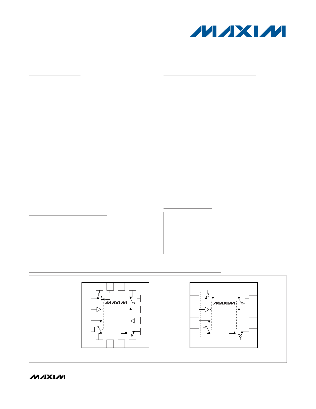
Pin Configurations
Ordering Information
19-2129; Rev 3; 4/11
For pricing, delivery, and ordering information, please contact Maxim Direct at 1-888-629-4642,
or visit Maxim’s website at www.maxim-ic.com.
Pin Configurations continued at end of data sheet.
+
Denotes a lead(Pb)-free/RoHS-compliant package.
*
EP = Exposed pad.
TOP VIEW
COM1
NO1 V+ NC4
16 15 14 13
++
PART TEMP RANGE PIN-PACKAGE
MAX4699ETE+ -40°C to +85°C 16 TQFN-EP* (4mm x 4mm)
MAX4701EUE+ -40°C to +85°C 16 TSSOP
MAX4701ETE+ -40°C to +85°C 16 TQFN-EP* (3mm x 3mm)
MAX4702EUE+ -40°C to +85°C 16 TSSOP
MAX4702ETE+ -40°C to +85°C 16 TQFN-EP* (3mm x 3mm)
COM1
NO1 V+ NC4
16 15 14 13
NC1
1
IN1, IN2
2
*MAX4701/MAX4702
ARE IN A
3mm x 3mm
TQFN PACKAGE
**CONNECT EXPOSED PAD TO GND.
NO2
COM2
3
4
MAX4699/
MAX4701*
**EP
8765
NC2 GND NO3 COM3
COM4
12
NO4
11
1N3, IN4
10
NC3
9
NC1
NO2
COM2
1
IN
2
3
4
MAX4702*
**EP
8765
NC2 GND NO3 COM3
TQFNTQFN
COM4
12
NO4
11
V
10
L
NC3
9
MAX4699/MAX4701/MAX4702
Low-Voltage, Dual DPDT/Quad SPDT
Analog Switches in QFN
2 _______________________________________________________________________________________
ABSOLUTE MAXIMUM RATINGS
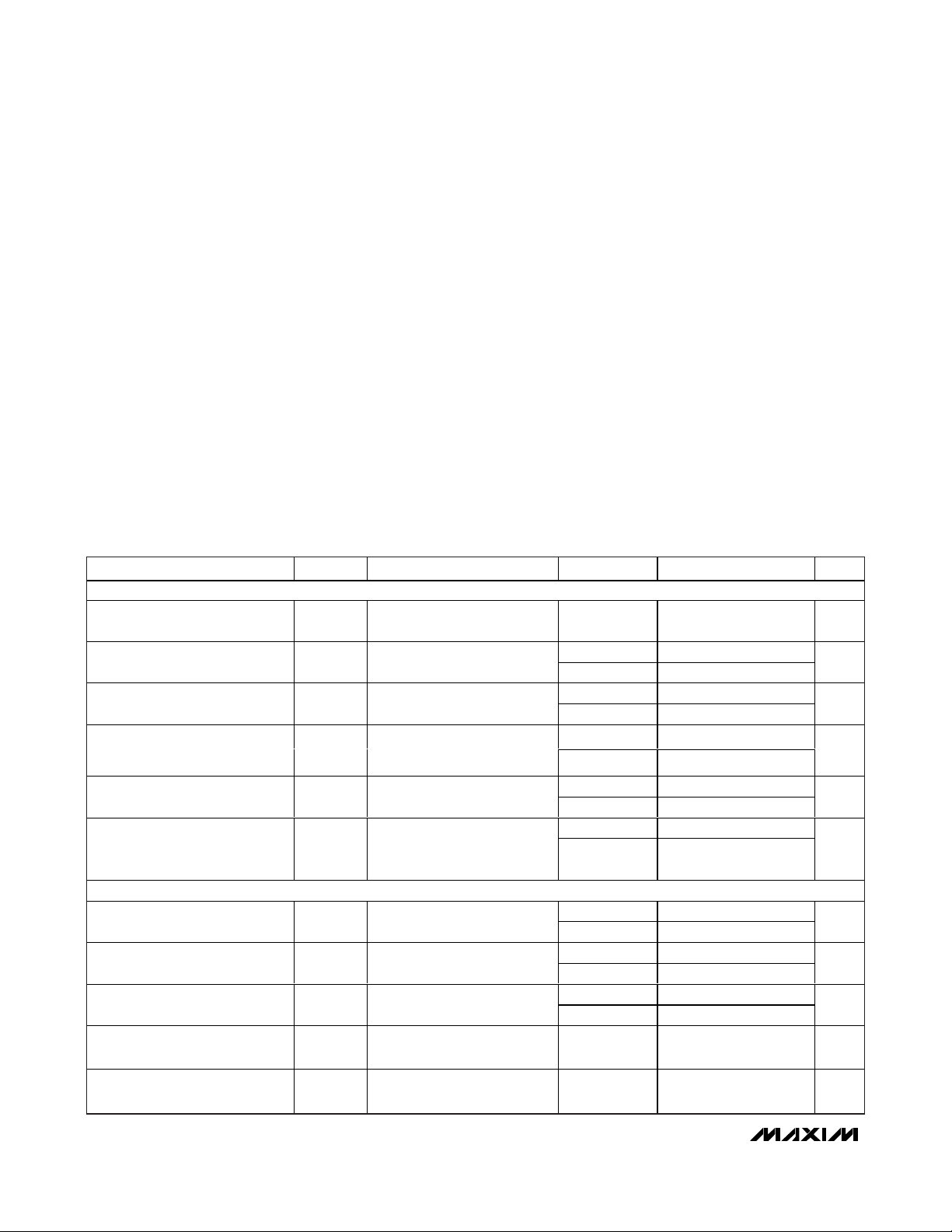
ELECTRICAL CHARACTERISTICS—Single +3V Supply
(V+ = +2.7V to +3.3V, V
GND
= 0V, VIH= +1.4V, VIL= +0.5V, (VL= +1.5V, VIH= +1.0V, VIL= +0.4V for MAX4702 only), TA= -40°C to
+85°C. Typical values are at V+ = +3V and T
A
= +25°C, unless otherwise noted.) (Notes 2, 3)
Stresses beyond those listed under “Absolute Maximum Ratings” may cause permanent damage to the device. These are stress ratings only, and functional
operation of the device at these or any other conditions beyond those indicated in the operational sections of the specifications is not implied. Exposure to
absolute maximum rating conditions for extended periods may affect device reliability.
(Voltages Referenced to GND)
V+............................................................................-0.3V to +6V
V
L
, IN_, COM_, NO_, NC_ (Note1).............. -0.3V to (V+ + 0.3V)
Continuous Current COM_, NO_, NC_ ............................ ±20mA
Peak Current COM_, NO_, NC_
(pulsed at 1ms, 10% duty cycle).................................±40mA
Continuous Power Dissipation (T
A
= +70°C)
TSSOP (derate 9.4mW/°C above +70°C) ...............754.7mW
16-Pin TQFN (derate 20.8mW/°C
above +70°C).........................................................1666.7mW
16-Pin Thin QFN (derate 25mW/°C
above +70°C)............................................................2000mW
Operating Temperature Range .......................... -40°C to +85°C
Storage Temperature Range ........................... -65°C to +150°C
Lead Temperature (soldering, 10s) ............................... +300°C
Soldering Temperature (reflow) .......................................+260°C
Note 1: Signals on IN_, COM_, NO_, and NC_ exceeding 0 or V+ are clamped by internal diodes. Limit forward-diode current to
maximum current rating.
)
)
)
PARAMETER SYMBOL CONDITIONS T
ANALOG SWITCH
Analog Signal Range
O n- Resi stance R
O n- Resi stance M atch Betw een
C hannel s ( N ote 4)
O n- Resi stance Fl atness ( N ote 5) R
N O_, N C _ O ff- Leakag e C ur r ent
( N ote 6)
COM_ On-Leakage Current
(Note 6)
DYNAMIC
Turn-On Time t
Turn-Off Time t
Break-Before-Make (Note 6) t
On-Channel -3dB Bandwidth BW
V
NO_
I
NO_(OFF)
I
NC_(OFF
I
COM_ (ON
,
V
COM_
, V
NC_
ON
ΔR
ON
FLAT (ON
V+ = +2.7V, I
V
or V
NO_
NC_
V+ = +2.7V, I
or V
V
NO_
NC_
V+ = +2.7V, I
or V
V
NO_
NC_
COM_
= +1.5V
COM_
= +1.5V
COM_
= +1V,
= 10mA;
= 10mA;
= 10mA;
+1.5V, +2V
,
V+ = +3.3V, V
+3V; V
NO_
or V
V+ = +3.3V, V
+3V; V
NO_
or V
COM_
NC_
COM_
NC_
= +1V,
= +3V, +1V
= +1V,
= +1V,
+3V, or unconnected
V
ON
OFF
BBM
or V
NO_
300Ω, C
V
or V
NO_
300Ω, C
V
or V
NO_
300Ω, C
= +2V; RL =
NC_
= 35pF, Figure 2
L
= +2V; RL =
NC_
= 35pF, Figure 2
L
= +2V; RL =
NC_
= 35pF, Figure 2
L
A
+25°C 60 75
T
to T
MIN
MAX
+25°C 2 4
to T
T
MIN
MAX
+25°C 8 12
T
to T
MIN
MAX
+25°C -0.5 +0.5
to T
T
MIN
MAX
+25°C -0.5 +0.5
T
to T
MIN
MAX
+25°C 27 35
to T
T
MIN
MAX
+25°C 15 20
to T
T
MIN
MAX
+25°C 15
T
to T
MIN
MAX
Signal = 0dBm, 50Ω
in and out, Figure 5
MIN TYP MAX UNITS
0V+V
85
5
14
-1 1
-1 1
45
25
1
250 MHz
Ω
Ω
Ω
nA
nA
ns
ns
ns
Off-Isolation (Note 7) V
ISO
f = 1MHz, RL = 50Ω,
C
= 5pF, Figure 5
L
+25°C -76 dB
MAX4699/MAX4701/MAX4702MAX4699/MAX4701/MAX4702
Low-Voltage, Dual DPDT/Quad SPDT
Analog Switches in QFN
Low-Voltage, Dual DPDT/Quad SPDT
Analog Switches in QFN
_______________________________________________________________________________________ 3
ELECTRICAL CHARACTERISTICS—Single +3V Supply (continued)
(V+ = +2.7V to +3.3V, V
GND
= 0V, VIH= +1.4V, VIL= +0.5V, (VL= +1.5V, VIH= +1.0V, VIL= +0.4V for MAX4702 only), TA= -40°C to
+85°C. Typical values are at V+ = +3V and T
A
= +25°C, unless otherwise noted.) (Notes 2, 3)
)
)
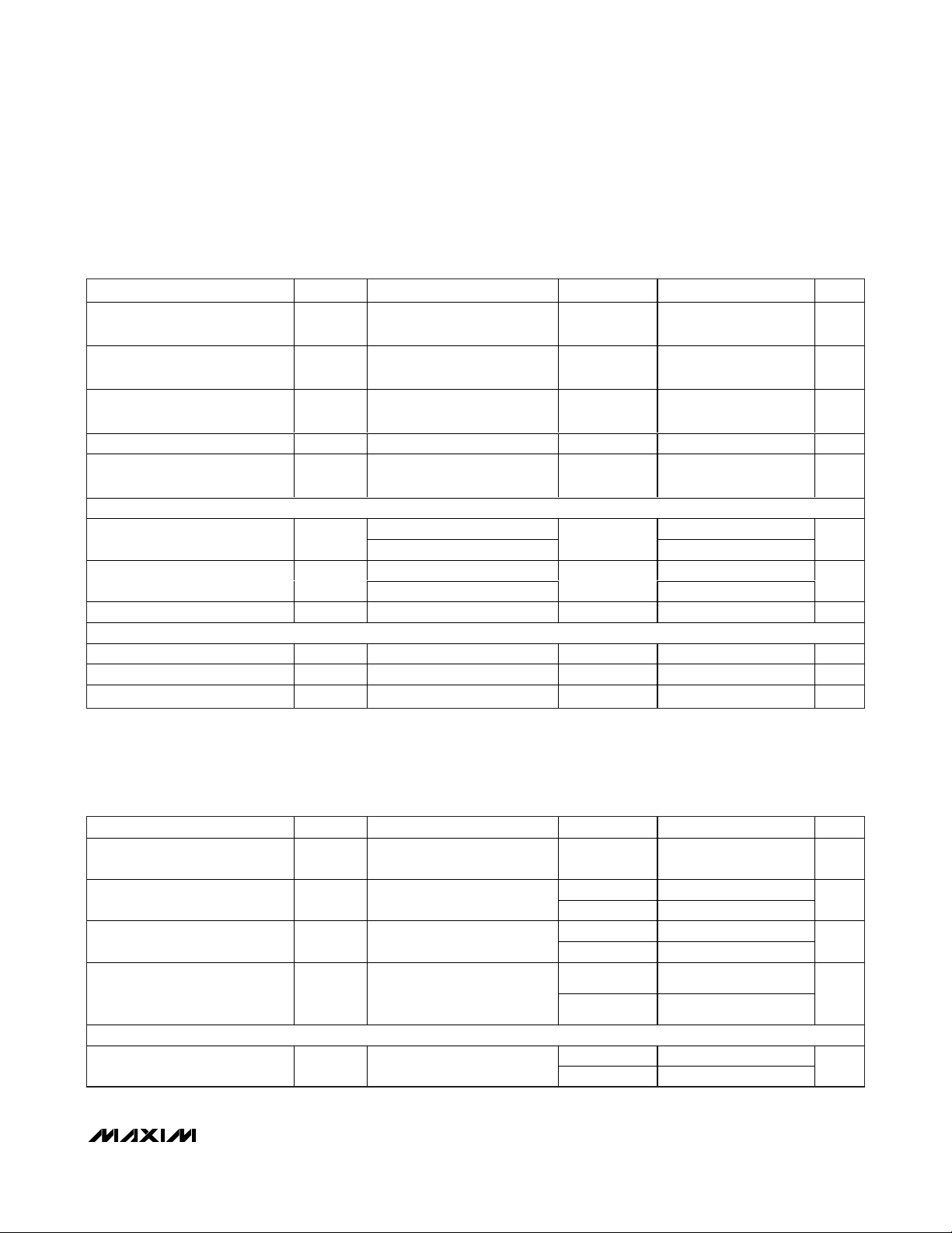
ELECTRICAL CHARACTERISTICS—Single +5V Supply
(V+ = +5V ±10%, V
GND
= 0V, VIH= +2.4V, VIL= +0.8V, (VL= +1.5V, VIH= +1.0V, VIL= +0.4V for MAX4702 only), TA= -40°C to
+85°C. Typical values are at V+ = +5V and T
A
= +25°C, unless otherwise noted.) (Notes 2, 3)
)
PARAMETER SYMBOL CONDITIONS T
Crosstalk (Note 8) V
Charge Injection Q
NO_, NC_, Off-Capacitance
Switch On-Capacitance C
Total Harmonic Distortion THD
DIGITAL I/O
Input Logic High V
Input Logic Low V
Input Leakage Current IIH, I
SUPPLY
Power-Supply Range V+ 1.8 5.5 V
Logic Power-Supply Input V
Positive Supply Current I+ V+ = +3.3V, VIN = 0 or V+ T
C
NO_(OFF
C
CT
NC_(OFF
(ON)
IH
IL
f = 1MHz, RL = 50Ω,
= 5pF, Figure 5
C
L
V
= 0V, R
GEN
C
= 1.0nF, Figure 4
L
,
f = 1MHz, V
= GND, Figure 6
V
NC_
f = 1MHz, Figure 6 +25°C 20 pF
f = 20Hz to 20kHz, 2.5Vp-p,
R
= 600Ω
L
MAX4699/MAX4701 1.4
MAX4702 (VL = +1.5V) 1.0
MAX4699/MAX4701 0.8
MAX4702 (VL = +1.5V) 0.4
VIN = 0 to V+ -1 1 µA
IL
L
GEN
NO_
= 0Ω,
,
A
+25°C -79 dB
+25°C 0.5 pC
+25°C 8 pF
+25°C 0.02 %
to T
MIN
MAX
MIN TYP MAX UNITS
1.5 V+ V
-1 1 µA
V
V
PARAMETER SYMBOL CONDITIONS T
Analog Signal Range
O n- Resi stance R
O n- Resi stance M atch Betw een
C hannel s ( N ote 4)
O n- Resi stance Fl atness ( N ote 5) R
DYNAMIC
Turn-On Time t
V
V
NO_
FLAT (ON
,
COM_
, V
NC_
ΔR
ON
ON
ON
V+ = +4.5V, I
V
or V
NO_
V+ = +4.5V, I
V
NO_
V+ = +4.5V, I
V
NO_
+2.25V, +3.5V
V
NO_
300Ω, C
NC_
or V
NC_
or V
NC_
or V
NC_
= 35pF, Figure 2
L
= 10mA;
COM_
= +3.5V
= 10mA;
COM_
= +3.5V
= 10mA;
COM_
= +2.0V,
= +3V; RL =
A
+25°C 30 40
T
to T
MIN
MAX
+25°C 1 3
to T
T
MIN
MAX
+25°C 5 8
to T
T
MIN
MAX
+25°C 15 18
to T
T
MIN
MAX
MIN TYP MAX UNITS
0V+V
50
10
20
Ω
5
Ω
Ω
ns
MAX4699/MAX4701/MAX4702
Low-Voltage, Dual DPDT/Quad SPDT
Analog Switches in QFN
4 _______________________________________________________________________________________
ELECTRICAL CHARACTERISTICS—Single +5V Supply (continued)
(V+ = +5V ±10%, V
GND
= 0V, VIH= +2.4V, VIL= +0.8V, (VL= +1.5V, VIH= +1.0V, VIL= +0.4V for MAX4702 only), TA= -40°C to
+85°C. Typical values are at V+ = +5V and T
A
= +25°C, unless otherwise noted.) (Notes 2, 3)
Note 2: The algebraic convention, where the most negative value is a minimum and the most positive value a maximum, is used in
this data sheet.
Note 3: -40°C specifications are guaranteed by design.
Note 4: ΔR
ON
= R
ON(MAX)
- R
ON(MIN)
.
Note 5: Flatness is defined as the difference between the maximum and minimum value of on-resistance as
measured over the specified analog signal ranges.
Note 6: Guaranteed by design.
Note 7: Off-Isolation = 20log10 (V
COM_
/ VNO), V
COM
= output, VNO= input to off switch.
Note 8: Between any two switches.
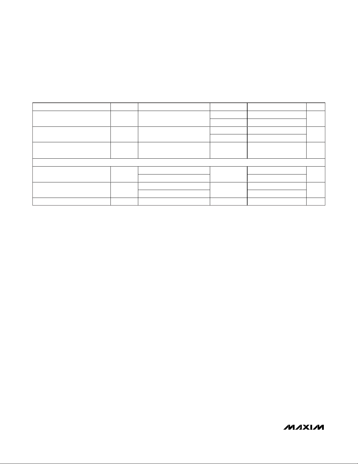
Turn-Off Time t
Break-Before-Make (Note 6) t
Charge Injection Q
DIGITAL I/O
Input Logic High V
Input Logic Low V
Logic Input Current IIH, I
PARAMETER SYMBOL CONDITIONS T
V
OFF
BBM
IH
IL
IL
or V
NO_
300Ω, C
V
or V
NO_
300Ω, C
V
GEN
C
= 1.0nF, Figure 4
L
MAX4699/MAX4701 2.4
MAX4702 (VL = +1.5V) 1.0
MAX4699/MAX4701 0.8
MAX4702 (VL = +1.5V) 0.4
VIN = 0 to V+ -1 1 µA
= +3V; RL =
NC_
= 35pF, Figure 2
L
= +3V; RL =
NC_
= 35pF, Figure 2
L
= 0V, R
GEN
= 0Ω,
A
+25°C 7 12
to T
T
MIN
MAX
+25°C 10
to T
T
MIN
MAX
+25°C 0.5 pC
MIN TYP MAX UNITS
2
15
ns
ns
V
V

Low-Voltage, Dual DPDT/Quad SPDT
Analog Switches in QFN
(TA= +25°C, unless otherwise noted. V
ON-RESISTANCE vs. COM VOLTAGE
OVER SUPPLY VOLTAGE
120
110
100
90
80
70
(Ω)
60
ON
R
50
40
30
20
10
I
0
01 3 5
COM
= 10mA
V+ = +1.8V
V+ = +2.7V
V+ = +3.3V
V+ = +5V
24
V
(V)
COM
ON-RESISTANCE vs. COM VOLTAGE
OVER TEMPERATURE (V+ = +5V)
40
30
TA = +25°C
TA = +85°C
= +1.5V for MAX4702 only.)
L
ON-RESISTANCE vs. COM VOLTAGE
OVER TEMPERATURE (V+ = +2.7V)
80
70
MAX4699 toc01
(Ω)
ON
R
TA = +25°C
60
50
40
30
20
V+ = +2.7V
10
= 10mA
I
COM
0
0 1.00.5 1.5 2.0 2.5
ON-LEAKAGE CURRENT
vs. TEMPERATURE
1000
MAX4699 toc04
100
Typical Operating Characteristics
ON-RESISTANCE vs. COM VOLTAGE
OVER TEMPERATURE (V+ = +3.3V)
V
COM
TA = -40°C
(V)
TA = +85°C
MAX4699 toc02
MAX4699 toc05a
(Ω)
ON
R
60
50
40
30
20
10
1000
100
TA = +25°C
V+ = +3.3V
= 10mA
I
COM
0
0 1.5 2.00.5 1.0 2.5 3.0
V
COM
TA = +85°C
TA = -40°C
(V)
OFF-LEAKAGE CURRENT
vs. TEMPERATURE
MAX4699/MAX4701/MAX4702
MAX4699 toc03
MAX4699 toc05b
(Ω)
20
ON
R
10
V+ = +5V
= 10mA
I
COM
0
021 345
V
COM
TA = -40°C
(V)
CHARGE INJECTION vs. COM VOLTAGE
OVER SUPPLY VOLTAGE
5
4
3
2
CHARGE INJECTION (pC)
1
0
021345
V+ = +3V
V
COM
(V)
I
COM
V+ = +5V
= 10mA
_______________________________________________________________________________________ 5
10
SUPPLY CURRENT (pA)
0.1
1000
100
MAX4699 toc06
10
0.1
SUPPLY CURRENT (nA)
0.01
0.001
1
V+ = +2.7V
-40 20-20 0 40 60 80
TEMPERATURE (°C)
SUPPLY CURRENT vs.
TEMPERATURE
1
-40 20 40-20 0 60 80
TEMPERATURE (°C)
10
1
OFF-LEAKAGE CURRENT (pA)
0.1
-40 20-20 0 40 60 80
1000
100
MAX4699 toc07
10
1
0.1
0.01
0.001
SUPPLY CURRENT (μA)
0.0001
0.00001
0.000001
0 1.00.5 1.5 2.0 2.5
TEMPERATURE (°C)
SUPPLY CURRENT vs.
LOGIC INPUT VOLTAGE
MAX4701
LOGIC INPUT VOLTAGE (V)
V+ = +2.7V
V+ = +2.7V
MAX4699 toc08

Low-Voltage, Dual DPDT/Quad SPDT
Analog Switches in QFN
Typical Operating Characteristics (continued)
(TA= +25°C, unless otherwise noted. V
= +1.5V for MAX4702 only.)
L
TURN-ON/OFF TIME
vs. SUPPLY VOLTAGE
30
25
20
(ns)
OFF
15
/t
ON
t
10
5
0
2.7 4.2 4.73.2 3.7 5.2
t
ON
t
OFF
SUPPLY VOLTAGE (V)
MAX4699 toc09
40
35
30
25
(ns)
OFF
/t
20
ON
t
15
10
5
-40 0 20-20 40 60 80
TURN-ON/OFF TIME
vs. TEMPERATURE
V+ = +2.7V
t
ON
t
OFF
TEMPERATURE (°C)
FREQUENCY RESPONSE
0
-20
-40
MAX4699/MAX4701/MAX4702
-60
LOSS (dB)
-80
ON-REPONSE
MAX4699 toc12
OFF-ISOLATION
CROSSTALK
0.1
0.01
THD (%)
LOGIC THRESHOLD vs. V
1.6
MAX4702
1.4
MAX4699 toc10
LOGIC THRESHOLD (V)
1.2
1.0
0.8
0.6
0.4
0.2
0
12345
VIN RISING
TOTAL HARMONIC DISTORTION
vs. FREQUENCY
RL = 600Ω
L
V+ = +5V
MAX4699 toc11
VIN FALLING
VL (V)
MAX4699 toc13
-100
-120
0.1 101 100 1000
FREQUENCY (MHz)
0.001
10 1k100 10k 100k
FREQUENCY (Hz)
6 _______________________________________________________________________________________

Detailed Description
The MAX4699/MAX4701 are low-voltage CMOS analog
switches that operate from a single +1.8V to +5.5V
power supply. The MAX4702 requires an additional
logic supply that allows for setting lower logic thresholds. The MAX4699/MAX4701 are double-pole/doublethrow (DPDT) devices. The MAX4702 is a quad
single-pole/double-throw (SPDT) device. These devices
feature a break-before-make switching, fast switching
speeds (with V+ = 5V: tON= 18ns max, t
OFF
= 9ns max
and with V+ = 3V: tON= 35ns, t
OFF
= 20) and rail-to-rail
signal handling. A logic input on the MAX4702 allows
for logic thresholds as low as 1.0V.
Applications Information
Analog Signal Levels
Analog signals that range over the entire supply voltage
(V+ to GND) can be passed with very little change in onresistance (see
Typical Operating Characteristics
). The
switches are bidirectional, so the NO, NC, and COM pins
can be used as either inputs or outputs.
_______________________________________________________________________________________ 7
MAX4699/MAX4701/MAX4702
Low-Voltage, Dual DPDT/Quad SPDT
Analog Switches in QFN
Pin Description
Figure 1. Overvoltage Protection Using Two External Blocking
Diodes
TQFN-EP PIN TS SOP PIN
MAX4699/
MAX4 701
1 1 3 3 NC1 Analog Switch 1—Normally Closed Terminal
— 2 — 4 IN Digital Control Input Switch 1, 2, 3, and 4
2 — 4 — IN1, IN2 Digital Control Input Switch 1 and 2
3 3 5 5 NO2 Analog Switch 2—Normall y Open Termina l
4 4 6 6 COM2 Analog Switch 2—Common Terminal
5 5 7 7 NC2 Analog Switch 2—Normally Closed Terminal
6 6 8 8 GND Ground
7 7 9 9 NO3 Analog Switch 3—Normall y Open Termina l
8 8 10 10 COM3 Analog Switch 3—Common Terminal
9 9 11 11 NC3 Analog Switch 3—Normally Clo sed Termina l
— 10 — 12 VL Logic Power-Supply Input
10 — 12 — IN3, IN4 Digital Control Input Switch 3 and 4
11 11 13 13 NO4 Analog Switch 4—Normally Open Terminal
12 12 14 14 COM4 Analog Switch 4—Common Terminal
13 13 15 15 NC4 Analog Switch 4—Normally Closed Terminal
14 14 16 16 V+ Posit ive Supply Voltage Input
15 15 1 1 NO1 Analog Switch 1—Norma ll y Open Termina l
16 16 2 2 COM1 Analog Switch 1—Common Terminal
— — — — EP Exposed Pad (TQFN Only). Connect EP to GND.
MAX4 702 MAX4701 MAX4702
NAME FUNCTION
POSITIVE SUPPLY
D1
V+
MAX4699
MAX4701
NO
V
g
GND
COM
D2
MAX4702

MAX4699/MAX4701/MAX4702
Power-Supply Sequencing and
Overvoltage Protection
Caution: Do not exceed the absolute maximum ratings because stresses beyond the listed ratings
may cause permanent damage to the devices.
Proper power-supply sequencing is recommended for
all CMOS devices. Always apply V+ before applying
analog signals, especially if the analog signal is not current limited. If this sequencing is not possible, and if the
analog inputs are not current limited to <20mA, add a
small-signal diode (D1) as shown in Figure 1. If the analog signal can dip below GND, add D2. Adding protection diodes reduces the analog range to a diode drop
(about 0.7V) below V+ (for D1), and a diode drop above
ground (for D2). On-resistance increases slightly at low
supply voltages. Maximum supply voltage (V+) must not
exceed +6V.
Adding protection diode D2 causes the logic threshold
to be shifted relative to GND. TTL compatibility is not
guaranteed when D2 is added.
Protection diodes D1 and D2 also protect against some
overvoltage situations. With Figure 1’s circuit, if the supply voltage is below the absolute maximum rating, and
if a fault voltage up to the absolute maximum rating is
applied to an analog signal pin, no damage will result.
VLLogic Input (MAX4702)
The MAX4702 features a VLlogic input that allows for
lower logic input thresholds down to 1.0V min for VIHin
the quad SPDT configuration. Power-up V
L
after V+ has
been powered with a minimum of 1.5V to ensure proper
operation of the device.
Low-Voltage, Dual DPDT/Quad SPDT
Analog Switches in QFN
8 _______________________________________________________________________________________
Figure 2. Switching Time
Figure 3. Break-Before-Make Interval
Test Circuits/Timing Diagrams
MAX4699
MAX4701
MAX4702
NO_
V
N_
OR NC_
LOGIC
INPUT
IN_
GND
V+
V+
COM_
R
L
300Ω
C
L
35pF
LOGIC
INPUT
V
OUT
SWITCH
OUTPUT
V
IH
V
IL
0
V
t
50%
OUT
ON
0.9 x V
0UT
tr < 5ns
tf < 5ns
t
OFF
0.9 x V
OUT
C
INCLUDES FIXTURE AND STRAY CAPACITANCE.
L
OUT
= V
N_ (
R
V
RL + R
L
)
ON
LOGIC INPUT WAVEFORMS INVERTED FOR SWITCHES
THAT HAVE THE OPPOSITE LOGIC SENSE.
GND
V+
V+
V
R
L
300Ω
OUT
C
35pF
L
COM_
LOGIC
INPUT
V
OUT
V
IH
V
IL
50%
0.9 x V
t
D
MAX4699
MAX4701
MAX4702
LOGIC
INPUT
V
N_
NC_
NO_
IN_
C
INCLUDES FIXTURE AND STRAY CAPACITANCE.
L
OUT

MAX4699/MAX4701/MAX4702
Low-Voltage, Dual DPDT/Quad SPDT
Analog Switches in QFN
_______________________________________________________________________________________ 9
Figure 4. Charge Injection
Figure 5. On-Loss, Off-Isolation, and Crosstalk
Figure 6. Channel Off/On-Capacitance
Test Circuits/Timing Diagrams (continued)
Chip Information
SUBSTRATE CONNECTED TO GND
MAX4699
MAX4701
MAX4702
V
GEN
R
GEN
V OR V+
50Ω
IN_
NC_
NC_
OR NO_
GND
V+
V+
MAX4699
MAX4701
MAX4702
GND
IN
10nF
V
IL
COM_
NO_
TO V
V+
V+
COM_
IH
ΔV
OUT
V
OUT
V
OUT
C
L
V
IN
V
OUT
MEAS REF
IN_
OFF
IN_
NETWORK
ANALYZER
50Ω
50Ω 50Ω
OFF
50Ω
ON
ON
Q = (ΔV
IN DEPENDS ON SWITCH CONFIGURATION;
INPUT POLARITY DETERMINED BY SENSE OF SWITCH.
)(CL)
OUT
OFF-ISOLATION = 20log
ON-LOSS = 20log
CROSSTALK = 20log
OFF
OFF
V
OUT
V
IN
V
OUT
V
IN
V
OUT
V
IN
MEASUREMENTS ARE STANDARDIZED AGAINST SHORTS AT IC TERMINALS.
OFF-ISOLATION IS MEASURED BETWEEN COM_ AND "OFF" NO_ OR NC_ TERMINAL ON EACH SWITCH.
ON-LOSS IS MEASURED BETWEEN COM_ AND "ON" NO_ OR NC_TERMINAL ON EACH SWITCH.
CROSSTALK IS MEASURED FROM ONE CHANNEL TO ALL OTHER CHANNELS.
SIGNAL DIRECTION THROUGH SWITCH IS REVERSED; WORST VALUES ARE RECORDED.
10nF
COM_
V+
V+
MAX4699
MAX4701
MAX4702
CAPACITANCE
METER
f = 1MHz
NC_ or
NO_
GND
IN_
V
IL
OR
V
IH

MAX4699/MAX4701/MAX4702
Low-Voltage, Dual DPDT/Quad SPDT
Analog Switches in QFN
10 ______________________________________________________________________________________
Pin Configurations (continued)
PACKAGE TYPE PACKAGE CODE OUTLINE NO. LAND PATTERN NO.
16 TQFN-EP (4mm x 4mm) T1644+4
21-0139 90-0070
16 TQFN-EP (3mm x 3mm) T1633+4
21-0136 90-0031
16 TSSOP U16+2
21-0066 90-0117
Package Information
For the latest package outline information and land patterns (footprints), go to www.maxim-ic.com/packages. Note that a “+”, “#”, or
“-” in the package code indicates RoHS status only. Package drawings may show a different suffix character, but the drawing pertains to the package regardless of RoHS status.
TOP VIEW
MAX4701
1
NO1 V+
COM1
2
NC1
3
IN1, IN2
4
NO2
5
COM2
6
NC2
7
GND
8
TSSOP TSSOP
IN1,
IN3,
IN2
IN4
L — NC1–COM1, NC2–COM2
H — NO1–COM1, NO2–COM2
— L NC3–COM3, NC4–COM4
— H NO3–COM3, NO4–COM4
ON SWITCHES
16
15
14
13
12
11
10
9
NC4
COM4
NO4
1N3, IN4
NC3
COM3
NO3
NO1 V+
COM1
NC1
IN
NO2
COM2
NC2
GND
SWITCHES SHOWN FOR
LOGIC “0” INPUTS
MAX4702
1
2
3
4
5
6
7
8
IN ON SWITCHES
NC1–COM1, NC2–COM2
L
NC3–COM3, NC4–COM4
NO1–COM1, NO2–COM2
H
NO3–COM3, NO4–COM4
16
15
NC4
14
COM4
13
NO4
V
12
L
NC3
11
COM3
10
NO3
9

MAX4699/MAX4701/MAX4702
Low-Voltage, Dual DPDT/Quad SPDT
Analog Switches in QFN
Maxim cannot assume responsibility for use of any circuitry other than circuitry entirely embodied in a Maxim product. No circuit patent licenses are
implied. Maxim reserves the right to change the circuitry and specifications without notice at any time.
Maxim Integrated Products, 120 San Gabriel Drive, Sunnyvale, CA 94086 408-737-7600 ____________________
11
© 2011 Maxim Integrated Products Maxim is a registered trademark of Maxim Integrated Products, Inc.
Revision History
REVISION
NUMBER
2 10/09
3 4/11 Corrected part numbers in Ordering Information; updated Absolute Maximum Ratings. 1, 2
REVISION
DATE
DESCRIPTION
Added “Exposed pad” reference to the Ordering Information table, Pin Configurations,
and Pin Description table.
PAGES
CHANGED
1, 7
 Loading...