

19-0219; Rev 2; 6/94
EVALUATION KIT MANUAL
FOLLOWS DATA SHEET
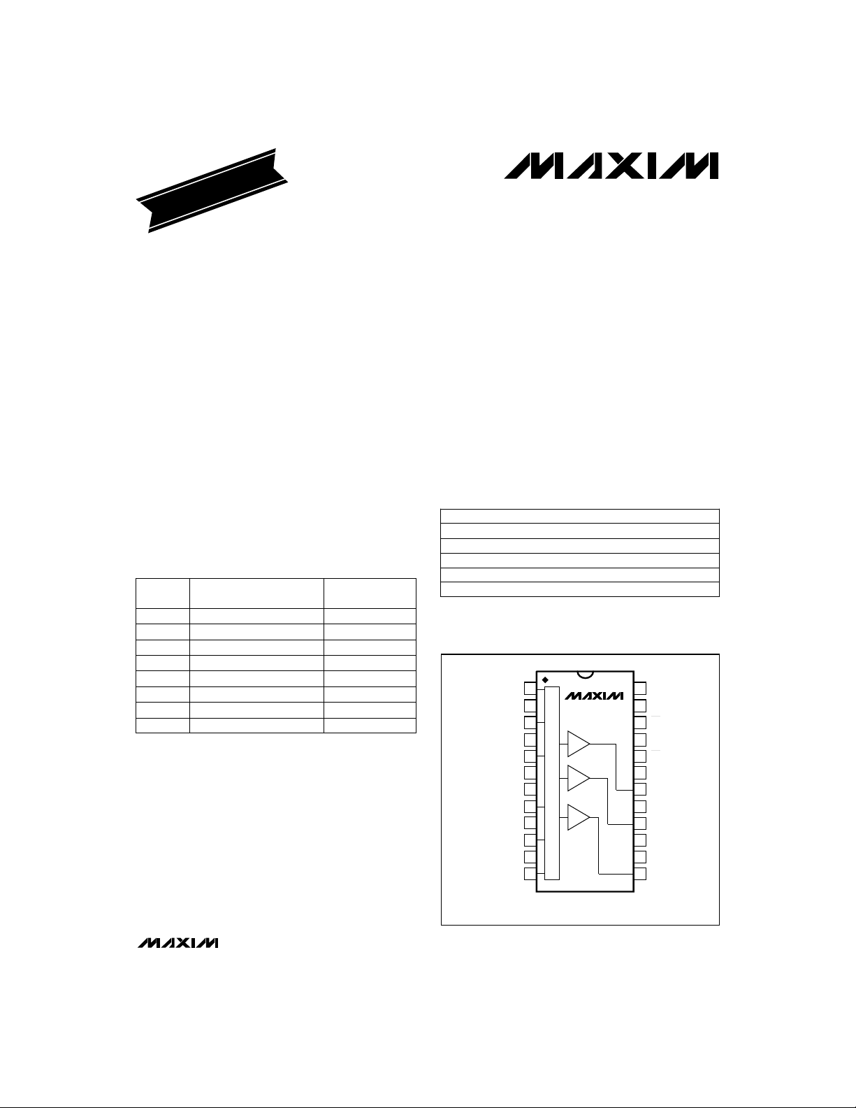
RGB Video Switches and Buffers
_______________General Description
The MAX463–MAX470 series of two-channel,
triple/quad buffered video switches and video buffers
combines high-accuracy, unity-gain-stable amplifiers
with high-performance video switches. Fast switching
time and low differential gain and phase error make this
series of switches and buffers ideal for all video applications. The devices are all specified for ±5V supply
operation with inputs and outputs as high as ±2.5V
when driving 150Ω loads (75Ω back-terminated cable).
Input capacitance is typically only 5pF, and channel-tochannel crosstalk is better than 60dB, accomplished by
surrounding all inputs with AC ground pins. The onboard amplifiers feature a 200V/µs slew rate (300V/µs
for AV= 2V/V amplifiers), and a bandwidth of 100MHz
(90MHz for AV= 2V/V buffers). Channel selection is
controlled by a single TTL-compatible input pin or by a
microprocessor interface, and channel switch time is
only 20ns.
For design flexibility, devices are offered with bufferamplifier gains of 1V/V or 2V/V for 75Ω back-terminated
applications. Output amplifiers have a guaranteed output swing of ±2V into 75Ω.
Devices offered in this series are as follows:
PART DESCRIPTION
MAX463 Triple RGB Switch & Buffer 1
MAX464 Quad RGB Switch & Buffer 1
MAX465 Triple RGB Switch & Buffer 2
MAX466 Quad RGB Switch & Buffer 2
MAX467 Triple Video Buffer 1
MAX468 Quad Video Buffer 1
MAX469 Triple Video Buffer 2
MAX470 Quad Video Buffer 2
VOLTAGE GAIN
(V/V)
________________________Applications
Broadcast-Quality Color-Signal Multiplexing
RGB Multiplexing
RGB Color Video Overlay Editors
RGB Color Video Security Systems
RGB Medical Imaging
Coaxial-Cable Line Drivers
Two-Channel, Triple/Quad
____________________________Features
♦ 100MHz Unity-Gain Bandwidth
♦ 90MHz Bandwidth with 2V/V Gain
♦ 0.01%/0.03° Differential Gain/Phase Error
♦ Drives 50Ω and 75ΩBack-Terminated Cable Directly
♦ Wide Output Swing:
±2V into 75Ω
±2.5V into 150Ω
♦ 300V/µs Slew Rate (2V/V gain)
♦ 20ns Channel Switching Time
♦ Logic Disable Mode:
High-Z Outputs
Reduced Power Consumption
♦ Outputs May Be Paralleled for Larger Networks
♦ 5pF Input Capacitance (channel on or off)
______________Ordering Information
PART TEMP. RANGE PIN-PACKAGE
MAX463CNG
MAX463CWG 0°C to +70°C 24 Wide SO
MAX463C/D 0°C to +70°C Dice*
MAX463ENG 24 Narrow Plastic DIP
MAX463EWG -40°C to +85°C 24 Wide SO
Ordering Information continued on last page.
* Dice are specified at T
_________________Pin Configurations
TOP VIEW
IN0A
IN1A
IN2A
IN0B
IN1B
IN2B
0°C to +70°C 24 Narrow Plastic DIP
-40°C to +85°C
= +25°C, DC parameters only.
A
1
GND
GND
GND
GND
2
3
4
5
V-
6
V-
7
8
9
10
11
12
MAX463
MAX465
3P2T SWITCH
24
GND
23
LE
22
EN
21
A0
20
CS
19
V-
18
OUT0
17
V+
16
OUT1
15
GND
14
V+
13
OUT2
MAX463–MAX470
Typical Operating Circuit appears at end of data sheet.
________________________________________________________________
Pin Configurations continued at end of data sheet.
DIP/SO
Maxim Integrated Products
Call toll free 1-800-998-8800 for free samples or literature.
1
Two-Channel, Triple/Quad
RGB Video Switches and Buffers
ABSOLUTE MAXIMUM RATINGS
Power-Supply Ranges
V+ to V- ................................................................................12V
Analog Input Voltage..........................(V- - 0.3V) to (V+ + 0.3V)
Digital Input Voltage...................................-0.3V to (V+ + 0.3V)
Output Short-Circuit Duration (to GND)........................1 Minute
Input Current into Any Pin, Power On or Off...................±50mA
Continuous Power Dissipation (T
16-Pin Plastic DIP (derate 22.22mW/°C above +70°C)....1778mW
16-Pin Wide SO (derate 20.00mW/°C above +70°C) .......1600mW
Stresses beyond those listed under “Absolute Maximum Ratings” may cause permanent damage to the device. These are stress ratings only, and functional
operation of the device at these or any other conditions beyond those indicated in the operational sections of the specifications is not implied. Exposure to
absolute maximum rating conditions for extended periods may affect device reliability.
= +70°C)
A
ELECTRICAL CHARACTERISTICS
(V+ = 5V, V- = -5V, -2V ≤ VIN≤ +2V, R
MAX463–MAX470
PARAMETER SYMBOL UNITS
Operating Supply Voltage V
Input Voltage Range
Offset Voltage V
Power-Supply Rejection Ratio PSRR 50 60 dB
On Input Bias Current I
On Input Resistance R
Input Capacitance C
Voltage-Gain Accuracy
Output Voltage Swing V
Output Impedance R
Output Resistance,
Disabled Mode
Output Capacitance,
Disabled Mode
Positive Supply Current I+
R
C
= 75Ω, unless otherwise noted.)
LOAD
CONDITIONS
S
V
IN
OS
BIAS
IN
Channel off or on
IN
MAX463/MAX464, MAX467/MAX468
(Note 1)
MAX465/MAX466, MAX469/MAX470,
R
= 150Ω, (Note 2)
LOAD
R
= 150Ω
OUT
OUT
OUTD
OUTD
LOAD
R
= 75Ω
LOAD
fIN= 10MHz
fIN= DC
MAX463/MAX464
MAX465/MAX466
MAX463–MAX466
MAX463/MAX465/MAX467/MAX469,
VIN= 0V
MAX464/MAX466/MAX468/MAX470,
VIN= 0V
MAX463/MAX465, disabled mode
MAX464/MAX466, disabled mode
24-Pin Narrow Plastic DIP
(derate 20.2mW/°C above +70°C)..................................1620mW
24-Pin Wide SO (derate 19.3mW/°C above +70°C) .........1590mW
28-Pin Narrow Plastic DIP
(derate 20.2mW/°C above +70°C)..................................1620mW
28-Pin Wide SO (derate 18.1mW/°C above +70°C) .........1440mW
Operating Temperature Ranges
MAX4_ _C_ _.........................................................0°C to +70°C
MAX4_ _E_ _......................................................-40°C to +85°C
Storage Temperature Range.............................-65°C to +150°C
Lead Temperature (soldering, 10sec).............................+300°C
MAX463/MAX464,
MAX467/MAX468
MAX465/MAX466,
MAX469/MAX470
TA= +25°C
MIN TYP MAX
±4.75 ±5 ±5.25 V
-2 2 V
±3 ±10 mV±15
±1 ±3 µA
300 700 kΩ
5 pF
0.2 0.5
0.3 1.0
±2.5 ±2.8
±2.0 ±2.4
5
0.05
0.1
150 250 kΩ
0.7 1 kΩ
10 pF
65 80
85 100
35 45
40 50
TA= T
to T
MIN
MIN MAX
±4.75 ±5.25
-2 2
50
150
±2.5
-1.5/+2
100
0.7
MAX
±5
1.0
2.0
100
120
50
55
%
V
Ω
mA
2 _______________________________________________________________________________________
Two-Channel, Triple/Quad
RGB Video Switches and Buffers
ELECTRICAL CHARACTERISTICS (continued)
(V+ = 5V, V- = -5V, -2V ≤ VIN≤ +2V, R
PARAMETER
Negative Supply Current
Input Noise Density en 20 nV/√–H—z
-3dB Bandwidth BW
Differential Gain Error
(Note 3)
Differential Phase Error
(Note 3)
Settling Time to 0.1%
Adjacent Channel Crosstalk
(Note 4)
All-Hostile Crosstalk (Note 5) XTALK 50 dB
All-Hostile Off Isolation (Note 6)
Channel Switching
Propagation Delay (Note 7)
Channel Switching Time
(Note 8)
Switching Transient 300 mV
Amplifier Switching Off-Time
(Note 9)
Amplifier Switching On-Time
(Note 10)
Logic Input High Threshold V
Logic Input Low Threshold V
Logic Input Current High I
Logic Input Current Low I
SYMBOL
XTALK
= 75Ω, unless otherwise noted.)
LOAD
CONDITIONS
MAX463/MAX465/MAX467/MAX469,
VIN= 0V
MAX464/MAX466/MAX468/MAX470,
I-
VIN= 0V
MAX463/MAX465, disabled mode
MAX464/MAX466, disabled mode
fIN= 10kHz
MAX463/MAX464, MAX467/MAX468
SR
MAX465/MAX466, MAX469/MAX470
MAX463/MAX464, MAX467/MAX468
MAX465/MAX466, MAX469/MAX470
MAX463/MAX464, MAX467/MAX468
DG
MAX465/MAX466, MAX469/MAX470
MAX463/MAX464, MAX467/MAX468
DP
MAX465/MAX466, MAX469/MAX470
t
VIN= 2V-to-0V step
S
fIN= 10MHz
fIN= 10MHz
ISO
fIN= 10MHz, MAX463–MAX466
t
MAX463–MAX466
PD
t
MAX463–MAX466
SW
V
= V
INA
t
MAX463–MAX466
OFF
t
ON
E—N–, A0, C—S–, LE; MAX463–MAX466
IH
E—N–, A0, C—S–, LE; MAX463–MAX466
IL
INHI
INLO
= 0V, MAX463–MAX466
INB
TA= +25°C
MIN TYP MAX
50 65
65 80
20 30
25 35
200
300
100
90
0.01
0.12
0.03
0.14
50 ns
60
70
15 ns
20 ns
80 ns
100 nsMAX463–MAX466
0.8 V
TA= T
2 V
200 µAE—N–, A0, C—S–, LE; MAX463–MAX466 200
200 µAE—N–, A0, C—S–, LE; MAX463–MAX466 200
to T
MIN
MIN MAX
75
95
35
40
2
0.8
MAX
UNITS
V/µsSlew Rate
MHz
deg.
MAX463–MAX470
mA
%
dB
dB
P-P
_______________________________________________________________________________________ 3
Two-Channel, Triple/Quad
RGB Video Switches and Buffers
ELECTRICAL CHARACTERISTICS (continued)
(V+ = 5V, V- = -5V, -2V ≤ VIN≤ +2V, R
PARAMETER
SYMBOL UNITS
Address Setup Time (Note 11) t
Address Hold Time (Note 11) t
C—S–Pulse Width Low (Note 11) t
Note 1: Voltage gain accuracy for the unity-gain devices is defined as [(V
Note 2: Voltage gain accuracy for the gain-of-two devices is defined as [(V
Note 3: Tested with a 3.58MHz sine wave of amplitude 40IRE superimposed on a linear ramp (0IRE to 100IRE), R
Note 4: Tested with the selected input connected to ground through a 75Ω resistor, and a 4V
Note 5: Tested in the same manner as described in Note 4, but with all other inputs driven.
Note 6: Tested with LE = 0V, E—N–= V+, and all inputs driven with a 4V
Note 7: Measured from a channel switch command to measurable activity at the output.
Note 8: Measured from where the output begins to move to the point where it is well defined.
Note 9: Measured from a disable command to amplifier in a non-driving state.
MAX463–MAX470
Note 10: Measured from an enable command to the point where the output reaches 90% current out.
Note 11: Guaranteed by design.
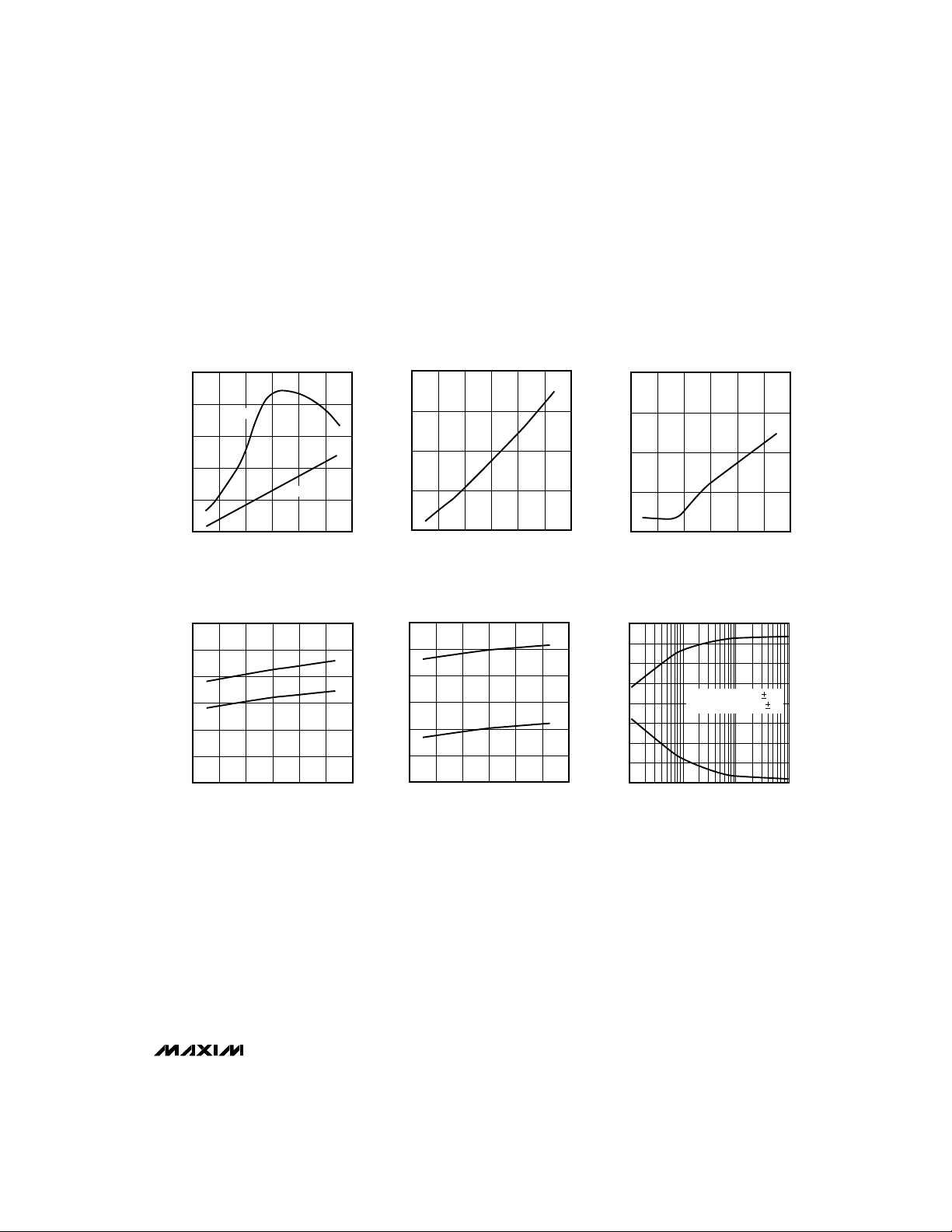
__________________________________________Typical Operating Characteristics
(TA = +25°C, unless otherwise noted.)
= 75Ω, unless otherwise noted.)
LOAD
CONDITIONS
SU
H
CS
MIN TYP MAX
30 nsE—N–, A0, C—S–, LE; MAX463–MAX466 30
15 nsE—N–, A0, C—S–, LE; MAX463–MAX466 15
- VIN) at VIN= 1V - (V
OUT
/2 - VIN) at VIN= 1V - (V
OUT
, 10MHz sine wave.
P-P
T
A
= +25°C
TA= T
to T
MIN
MIN MAX
MAX
0 nsE—N–, A0, C—S–, LE; MAX463–MAX466 0
- VIN) at VIN= -1V]/2.
OUT
/2 - VIN) at VIN= -1V]/2.
OUT
= 150Ω to ground.
sine wave at 10MHz driving adjacent input.
P-P
L
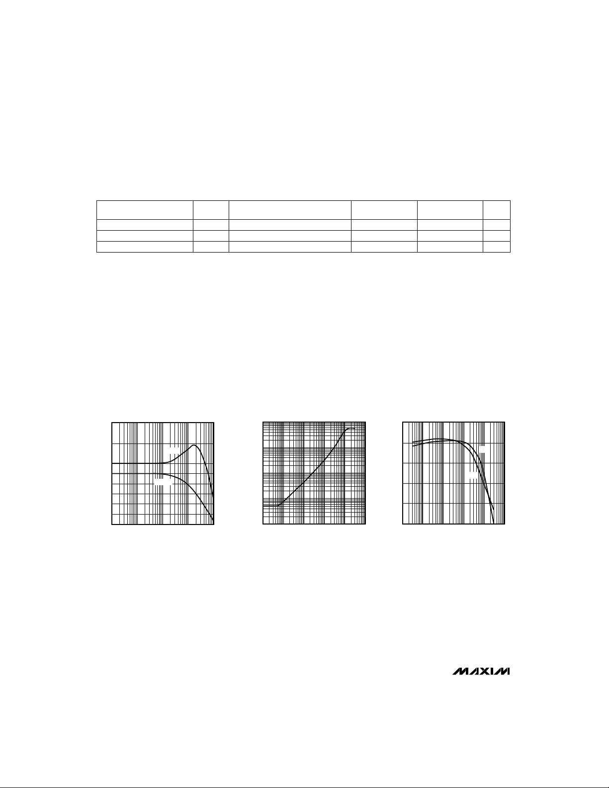
GAIN AND PHASE RESPONSES
2
1
0
GAIN (dB)
–1
–2
–3
10k 100k
FREQUENCY (Hz)
MAX468
GAIN
PHASE
1M 100M
10M
MAX463/470 -01
0
36
72
108
144
PHASE (DEGREES)
180
OUTPUT IMPEDANCE
100
Ω
10
1
OUTPUT IMPEDANCE ( )
0.1
0.01
vs. FREQUENCY
FREQUENCY (Hz)
MAX464
1M 100M
10M10k
MAX463/470 -02
1G100k
POWER-SUPPLY REJECTION RATIO
60
50
40
PSRR (dB)
30
20
10
1k 100k
vs. FREQUENCY
FREQUENCY (Hz)
4 _______________________________________________________________________________________
MAX468
1M 100M
MAX463/470 -03
V–
V+
10M10k
Two-Channel, Triple/Quad
RGB Video Switches and Buffers
____________________________Typical Operating Characteristics (continued)
(TA = +25°C, unless otherwise noted.)
VOLTAGE GAIN ACCURACY
0.16
0.14
0.12
0.10
PERCENTAGE (%)
0.08
0.06
30
25
20
15
10
5
SUPPLY CURRENT PER AMPLIFIER (mA)
0
–50
vs. TEMPERATURE
MAX465
MAX463
–25 0 5025 75–50
TEMPERATURE (°C)
SUPPLY CURRENT PER AMPLIFIER
vs. TEMPERATURE
I+
I–
–25 0 50
25 75
TEMPERATURE (°C)
MAX463/470 -04
100
MAX463/470 -09
100
DISABLED OUTPUT RESISTANCE
vs. TEMPERATURE
400
350
300
250
OUTPUT RESISTANCE (kΩ)
200
–25 0 5025 75–50
TEMPERATURE (°C)
DISABLED SUPPLY CURRENT
40
35
30
25
20
SUPPLY CURRENT (mA)
15
10
–50
vs. TEMPERATURE
I+
I–
–25 0 50
TEMPERATURE (°C)
MAX463
25 75
MAX463/470 -05
100
MAX463/470 -07
100
DISABLED OUTPUT RESISTANCE
1.30
1.25
1.20
1.15
OUTPUT RESISTANCE (kΩ)
1.10
4
3
2
1
0
–1
OUTPUT VOLTAGE (V)
–2
–3
–4
10 100
MAX465
vs. TEMPERATURE
–25 0 5025 75–50
TEMPERATURE (°C)
OUTPUT VOLTAGE SWING
vs. LOAD RESISTANCE
MAX463/4/7/8:VIN = 4V
MAX465/6/9/70:V
LOAD RESISTANCE ( )
1000 10000
= 2V
IN
Ω
MAX463–MAX470
MAX463/470 -06
100
MAX463/470 -08
_______________________________________________________________________________________
5

Two-Channel, Triple/Quad
RGB Video Switches and Buffers
____________________________Typical Operating Characteristics (continued)
(TA = +25°C, unless otherwise noted.)
SMALL-SIGNAL STEP RESPONSE
MAX464
GND
GND
MAX463–MAX470
10ns/div
MAX464
LARGE-SIGNAL STEP RESPONSE
GND
GND
20ns/div
,
A: V
IN
100mV/div
B: V
OUT
100mV/div
A: VIN,
2V/div
B: V
OUT
2V/div
SMALL-SIGNAL STEP RESPONSE
MAX466
,
A: V
GND
,
GND
10ns/div
IN
100mV/div
B: V
OUT
200mV/div
,
MAX466
LARGE-SIGNAL STEP RESPONSE
GND
GND
,
20ns/div
A: V
1V/div
B: V
2V/div
,
IN
,
OUT
OUTPUT TRANSIENT WHEN SWITCHING
BETWEEN TWO GROUNDED INPUTS
GND
GND
GND
50ns/div
A: CS,
5V/div
B: A0,
5V/div
C: OUT0,
100mV/div
GND
GND
GND
t
OFF
MAX464
EN RESPONSE TIME
t
ON
6 _______________________________________________________________________________________
MAX464
A: CS,
5V/div
B: EN,
5V/div
C: OUT3,
1V/div
50ns/div

Two-Channel, Triple/Quad
RGB Video Switches and Buffers
_____________________________________________________________Pin Descriptions
2, 4, 9,
11, 15, 24
20
22
PIN
MAX464/MAX466MAX463/MAX465
28 Channel A, Analog Input 0IN0A1
1, 3, 5,
11, 13, 19
2 Channel A, Analog Input 1IN1A3
4 Channel A, Analog Input 2IN2A5
6 Channel A, Analog Input 3IN3A–
7, 9, 21, 23 Negative Power-Supply Input. Connect to -5V. Thermal path.V-6, 7, 19
8 Channel B, Analog Input 0IN0B8
10 Channel B, Analog Input 1IN1B10
12 Channel B, Analog Input 2IN2B12
14 Channel B, Analog Input 3IN3B–
15 Buffered Analog Output 3OUT3–
17 Buffered Analog Output 2OUT213
16, 18 Positive Power-Supply Input. Connect to +5V.V+14, 17
20 Buffered Analog Output 1OUT116
22 Buffered Analog Output 0OUT018
24
25 A021
26
27 LE23
NAME
–C—S–
–E—N–
FUNCTION
Analog GroundGND
Chip-Select—latch control for the digital inputs. When –C—S– is low, A0 and E—N
input registers are transparent. When C—S– goes high, the A0 input register latches.
If LE is high, the E—N–input register also latches when C—S– goes high (see LE).
Channel-Select Input. When C—S–is low, driving A0 low selects channel A
and driving A0 high selects channel B.
Buffer-Enable Input. When C—S– is low or LE is low, driving E—N–low enables
all output buffers and driving E—N–high disables all output buffers.
Digital Latch-Enable Input. When LE is low, the E—N–register is transparent;
when LE is high, the E—N–register is transparent only when C—S– is low. Hardwire to V+ or GND for best crosstalk performance.
–
MAX463–MAX470
PIN
MAX468/MAX470MAX467/MAX469
1
2, 7, 15 Analog GroundGND2, 7, 8, 9, 15
3
4, 5, 12, 13 Negative Power-Supply Input. Connect to -5V. Thermal path.V-4, 5, 12, 13
6 Analog Input 2IN26
8 Analog Input 3IN3–
9 Buffered Analog Output 3OUT3–
10 Positive Power-Supply Input. Connect to +5V.V+10
11 Buffered Analog Output 2OUT211
14 Buffered Analog Output 1OUT114
16 Buffered Analog Output 0OUT016
_______________________________________________________________________________________
NAME
Analog Input 0IN01
Analog Input 1IN13
FUNCTION
7

Two-Channel, Triple/Quad
RGB Video Switches and Buffers
_______________Detailed Description
The MAX463–MAX470 have a bipolar construction,
which results in a typical channel input capacitance of
only 5pF, whether the channel is on or off. This low
input capacitance allows the amplifiers to realize full
AC performance, even with source impedances as
great as 250Ω. It also minimizes switching transients
because the driving source sees the same load
whether the channel is on or off. Low input capacitance is critical, because it forms a single-pole RC lowpass filter with the output impedance of the signal
source, and this filter can limit the system’s signal
bandwidth if the RC product becomes too large.
The MAX465/MAX466/MAX469/MAX470’s amplifiers are
internally configured for a gain of two, resulting in an overall gain of one at the cable output when driving back-ter-
MAX463–MAX470
minated coaxial cable (see the section
Cable
). The MAX463/MAX464/MAX467/MAX468 are
internally configured for unity gain.
Driving Coaxial
Power-Supply Bypassing and Board Layout
To realize the full AC performance of high-speed amplifiers, pay careful attention to power-supply bypassing
and board layout, and use a large, low-impedance
ground plane. With multi-layer boards, the ground
plane should be located on the layer that is not dedicated to a specific signal trace.
To prevent unwanted signal coupling, minimize the
trace area at the circuit's critical high-impedance
nodes, and surround the analog inputs with an AC
ground trace (analog ground, bypassed DC power
supply, etc). The analog input pins to the
MAX463–MAX470 have been separated with AC
ground pins (GND, V+, V-, or a hard-wired logic input)
to minimize parasitic coupling, which can degrade
crosstalk and/or stability of the amplifier. Keep signal
paths as short as possible to minimize inductance,
and ensure that all input channel traces are of equal
length to maintain the phase relationship between the
R, G, and B signals. Connect the coaxial-cable shield
to the ground side of the 75Ω terminating resistor at
the ground plane to further reduce crosstalk (see
Figure 1).
Bypass all power-supply pins directly to the ground
plane with 0.1µF ceramic capacitors, placed as close
to the supply pins as possible. For high-current loads,
it may be necessary to include 10µF tantalum or aluminum-electrolytic capacitors in parallel with the 0.1µF
ceramics. Keep capacitor lead lengths as short as
possible to minimize series inductance; surface-mount
(chip) capacitors are ideal.
COAX
COAX
Figure 1. Low-Crosstalk Layout. Return current from the
termination resistor does not flow through the ground plane.
Connect all V- pins to a large power plane. The V- pins
conduct heat away from the internal die, aiding thermal
dissipation.
Differential gain and phase errors are critical specifications for an amplifier/buffer in color video applications,
because these errors correspond directly to changes in
the color of the displayed picture in composite video
systems. The MAX467–MAX470 have low differential
gain and phase errors, making them ideal in broadcastquality composite color applications, as well as in RGB
video systems where these errors are less significant.
The MAX467–MAX470 differential gain and phase errors
are measured with the Tektronix VM700 Video
Measurement Set, with the input test signal provided by
the Tektronix 1910 Digital Generator as shown in Figure 2.
Measuring the differential gain and phase of the
MAX469/MAX470 (Figure 2a) is straightforward because
the output amplifiers are configured for a gain of two,
allowing connection to the VM700 through a back-terminated coaxial cable. Since the MAX467/MAX468 are
unity-gain devices, driving a back-terminated coax
would result in a gain of 1/2 at the VM700.
Figure 2b shows a test method to measure the differential gain and phase for the MAX467/MAX468. First,
measure and store the video signal with the device
under test (DUT) removed and replaced with a short
circuit, and the 150Ω load resistor omitted. Then do
another measurement with the DUT and load resistor in
the circuit, and calculate the differential gain and phase
errors by subtracting the results.
RT
RETURN
CURRENT
GROUND PLANE
RT
RETURN
CURRENT
Differential Gain and Phase Errors
8 _______________________________________________________________________________________

Two-Channel, Triple/Quad
RGB Video Switches and Buffers
(a)
75Ω
SOURCE:
TEKTRONIX
1910 DIGITAL GENERATOR
75Ω CABLE
(b)
75Ω
Figure 2. Differential Phase and Gain Error Test Circuits (a) for the MAX469/MAX470 Gain-of-Two Amplifiers, (b) for the
MAX467/MAX468 Unity-Gain Amplifiers
75Ω CABLE
MAX469/MAX470
DUT
MAX467/MAX468
DUT
150Ω
Driving Coaxial Cable
High-speed performance, excellent output current
capability, and an internally fixed gain of two make the
MAX465/MAX466/MAX469/MAX470 ideal for driving
50Ω or 75Ω back-terminated coaxial cables. The
MAX465/MAX466/MAX469/MAX470 will drive a 150Ω
75Ω CABLE
75Ω
75Ω CABLE
75Ω
75Ω
AV = 2
75Ω
MEASUREMENT:
TEKTRONIX VM700
VIDEO MEASUREMENT
SET
75Ω CABLE
75Ω
The MAX463–MAX470 phase margin and capacitiveload driving performance are optimized by internal
compensation. When driving capacitive loads greater
than 50pF, connect an isolation resistor between the
amplifier output and the capacitive load, as shown in
Figure 3.
load (75Ω back-terminated cable) to ±2.5V.
The
Typical Operating Circuit
shows the MAX465/MAX466
driving four back-terminated 75Ω video cables. The
back-termination resistor (at each amplifier output) provides impedance matching at the driven end of the
cable to eliminate signal reflections. It forms a voltage
divider with the load impedance, which attenuates the
signal at the cable output by one-half. The amplifier
operates with an internal 2V/V closed-loop gain to provide unity gain at the cable’s output.
AV = 1
12Ω
OUT_IN_
Driving Capacitive Loads
Driving large capacitive loads increases the likelihood
of oscillation in most amplifier circuits. This is especially
true for circuits with high loop-gains, like voltage followers. The amplifier’s output impedance and the capaci-
MAX468
tive load form an RC filter that adds a pole to the loop
response. If the pole frequency is low enough, as
when driving a large capacitive load, the circuit phase
margin is degraded and oscillation may occur.
Figure 3a. Using an Isolation Resistor with a Capacitive Load
MAX463–MAX470
100pF
_______________________________________________________________________________________ 9

Two-Channel, Triple/Quad
RGB Video Switches and Buffers
MAX468 (NO ISOLATION RESISTOR)
GND
GND
C
= 100pF
LOAD
, 500mV/div
A: V
MAX463–MAX470
B: V
IN
, 500mV/div
OUT
1µs/div
Figure 3b. Step Response without an Isolation Resistor
Digital Interface
The MAX463–MAX466 multiplexer architecture provides
an input transistor buffer, ensuring that no input channels are ever connected together. Select a channel by
changing A0's state (A0 = 0 for channel A, and A0 = 1
for channel B) and pulsing C—S–low (see Tables 1a, 1b).
Figure 4 shows the logic timing diagram.
Output Disable (MAX463–MAX466)
When the enable input (E—N–) is driven to a TTL low state, it
enables the MAX463–MAX466 amplifier outputs. When E—N
is driven high, it disables the amplifier outputs. The
MAX468 (WITH ISOLATION RESISTOR)
A
B
GND
GND
C
A: V
B: V
LOAD
= 100pF, R
, 500mV/div
IN
, 500mV/div
OUT
ISOLATION
1µs/div
= 12Ω
Figure 3c. Step Response with an Isolation Resistor
A
B
disabled MAX463/MAX464 outputs exhibit a 250kΩ
typical resistance. Because their internal feedback
resistors are required to produce a gain of two, the
MAX465/MAX466 exhibit a 1kΩ disabled output resistance.
LE determines whether E—N–is latched by C—S–or operates
independently. When the latch-enable input (LE) is connected to V+, C—S–becomes the latch control for the E—N
input register. If C—S– is low, both the E—N–and A0 registers
–
are transparent; once C—S– returns high, both registers
–
are latched.
t
CS
A0
EN
OUTPUTS
LE = V+
CS
t
t
SU
t
H
t
t
SU
t
OFF
t
PD
SW
H
t
ON
HIGH-Z
Figure 4. Logic Timing Diagram
10 ______________________________________________________________________________________

Two-Channel, Triple/Quad
RGB Video Switches and Buffers
Table 1a. Amplifier and Channel Selection
with LE = V+
–
–
C—S
Enables amplifier outputs.
000
Selects channel A.
Enables amplifier outputs.
100
Selects channel B.
Disables amplifiers. Outputs high-Z.X10
Latches all input registers.
XX1
Changes nothing.
When LE is connected to ground, the E—N–register is
transparent and independent of C—S–activity. This allows
all MAX463–MAX466 devices to be simultaneously shut
down, regardless of the C—S–input state. Simply connect
LE to ground and connect all E—N–inputs together (Figure
5a). For the MAX464 and MAX466, LE must be hardwired to either V+ or ground (rather than driving LE with
a gate) to prevent crosstalk from the digital inputs to
IN0A.
FUNCTIONA0E—N
Table 1b. Amplifier and Channel Selection
with LE = GND
–
–
C—S
Enables amplifier outputs.
000
Selects channel A.
Enables amplifier outputs.
100
Selects channel B.
Disables amplifiers. Outputs high-Z.
010
A0 register = channel A
Disables amplifiers. Outputs high-Z.
110
A0 register = channel B
Enables amplifier outputs, latches A0
register, programs outputs to output A
X01
or B, according to the setting of A0 at
C—S–'s last edge.
Disables amplifiers. Outputs high-Z.X11
Another option for output disable is to connect LE to V+,
parallel the outputs of several MAX463-MAX466s, and use
E—N–to individually disable all devices but the one in use
(Figure 5b).
When the outputs are disabled, the off isolation from
the analog inputs to the amplifier outputs is typically
70dB at 10MHz, all inputs driven with a 4V
wave and a 150Ω load impedance. Figure 6 shows the
test circuits used to measure isolation and crosstalk.
FUNCTIONA0E—N
sine
P-P
MAX463–MAX470
+5V
+5V
EN
CS
EN
AO
CS
LE
AO
LE
MAX463–
MAX466
MAX463–
MAX466
(b)
MAX463–
MAX466
LE
SHUTDOWN
NOTE: ISOLATION RESISTORS,
IF REQUIRED, NOT SHOWN.
Figure 5. (a) Simultaneous Shutdown of all MAX463–MAX466, (b) Enable (–E—N–) Register Latched by –C—S
______________________________________________________________________________________ 11
EN
MAX463–
MAX466
LE
EN
(a)
–

Two-Channel, Triple/Quad
RGB Video Switches and Buffers
MAX467–MAX470
75Ω
VIN = 4V
P-P
AT 10MHz,
= 75Ω
R
S
MAX463–MAX470
*
(a) (b)
MAX463–MAX466
150Ω
150Ω
75Ω
75Ω
VIN = 4V
AT 10MHz,
= 75Ω
R
S
MAX467–MAX470
P-P
MAX463–MAX466
150Ω
*
150Ω
VIN = 4V
= 75Ω
R
S
150Ω
150Ω
*
150Ω
ENLE
AT 10MHz,
P-P
+5V
(c) (d)
* MAX464/MAX466/MAX468/MAX470 ONLY
VIN = 4V
R
= 75Ω
S
AT 10MHz,
P-P
*
150Ω
150Ω
150Ω
Figure 6. (a) MAX467–MAX470 Adjacent Channel Crosstalk, (b) MAX467–MAX470 All-Hostile Crosstalk, (c) MAX463–MAX466
All-Hostile Off Isolation, (d) MAX463–MAX466 All-Hostile Crosstalk
12 ______________________________________________________________________________________

Two-Channel, Triple/Quad
RGB Video Switches and Buffers
MAX463–MAX470
75Ω
75Ω
75Ω
75Ω
75Ω
75Ω
75Ω
75Ω
75Ω
75Ω
75Ω
75Ω
75Ω
75Ω
75Ω
75Ω
28
1
GND
2
IN1A
3
GND
4
IN2A
5
GND
6
IN3A
7
V–
–5V
8
IN0B
9
V–
–5V
10
IN1B
11
GND
12
IN2B
13
GND
14
IN3B
1
GND
2
IN1A
3
GND
4
IN2A
5
GND
6
IN3A
7
V–
–5V
8
IN0B
9
V–
–5V
10
IN1B
11
GND
12
IN2B
13
GND
14
IN3B
MAX464
4P2T VIDEO SWITCH
MAX464
4P2T VIDEO SWITCH
IN0A
OUT0
OUT1
GND
OUT2
OUT3
IN0A
OUT0
OUT1
GND
OUT2
OUT3
27
+5V
LE
26
EN
25
A0
24
CS
23
–5V
V–
22
75Ω
21
–5V
V–
20
75Ω
19
18
+5V
V+
17
75Ω
16
+5V
V+
15
75Ω
28
27
+5V
LE
26
EN
25
A0
24
CS
23
–5V
V–
22
75Ω
21
–5V
V–
20
75Ω
19
18
+5V
V+
17
75Ω
16
+5V
V+
15
75Ω
FROM OTHER
MAX464s
1
2
3
4
–5V
5
–5V
6
7
8
IN0
IN1
IN2
GND
IN3
MAX470
16
OUT0
75Ω
15
GNDGND
14
OUT1
75Ω
13
OUT2
OUT3
V–
–5V
12
V–
–5V
11
75Ω
10
V+
V+
9
75Ω
V–
V–
75Ω
75Ω
75Ω
75Ω
Figure 7. Higher-Order RGB + Sync Video Multiplexer
______________________________________________________________________________________ 13

Two-Channel, Triple/Quad
RGB Video Switches and Buffers
75Ω
1
GND
2
IN1A
75Ω
3
GND
4
IN2A
75Ω
5
GND
6
IN3A
75Ω
7
V–
–5V
8
IN0B
75Ω
9
MAX463–MAX470
75Ω
75Ω
75Ω
75Ω
75Ω
75Ω
75Ω
75Ω
75Ω
75Ω
75Ω
V–
–5V
10
11
12
13
14
1
2
3
4
5
6
7
–5V
8
9
–5V
10
11
12
13
14
IN1B
GND
IN2B
GND
IN3B
GND
IN1A
GND
IN2A
GND
IN3A
V–
IN0B
V–
IN1B
GND
IN2B
GND
IN3B
QUAD SPDT VIDEO SWITCH
QUAD SPDT VIDEO SWITCH
MAX466
MAX466
IN0A
OUT0
OUT1
GND
OUT2
OUT3
IN0A
OUT0
OUT1
GND
OUT2
OUT3
+5V
–5V
22Ω
–5V
22Ω
+5V
22Ω
+5V
22Ω
+5V
–5V
22Ω
–5V
22Ω
+5V
22Ω
+5V
22Ω
A1 A0 CS
50Ω
50Ω
50Ω
50Ω
75Ω
75Ω
75Ω
75Ω
28
27
LE
26
EN
25
A0
24
CS
23
V–
22
21
V–
20
19
18
V+
17
16
V+
15
28
27
LE
26
EN
25
A0
24
CS
23
V–
22
21
V–
20
19
18
V+
17
16
V+
15
Figure 8. 1-of-4 RGB + Sync Video Multiplexer
14 ______________________________________________________________________________________

Two-Channel, Triple/Quad
RGB Video Switches and Buffers
__________Applications Information
Higher-Order RGB + Sync
Video Multiplexing
Higher-order RGB video multiplexers can be realized
by paralleling several MAX463/MAX464s. Connect LE
to V+ and use C—S– and E—N–to disable all devices but the
one in use. Since the disabled output resistance of the
MAX463/MAX464 is 250kΩ, several devices may be
paralleled to form larger RGB video multiplexer arrays
without signal degradation. Connect series resistors at
each amplifier's output to isolate the disabled output
capacitance of each paralleled device, and use a
MAX469 or MAX470 to drive the output coaxial cables
(see Figure 7).
Figure 8 shows a 1-of-4 RGB + sync video mux/amp
circuit. The 1kΩ disabled output resistance limits the
number of paralleled MAX465/MAX466s to no more
than two. The amplifier outputs are connected after a
22Ω isolation resistor and ahead of a 50Ω back-termination resistor, which isolates the active amplifier output from the capacitive load (5pF typ) presented by the
inactive output of the second MAX466. Impedance
mismatching is minimal, and the signal gain at the
cable end is near 1. This minimizes ringing in the output signals. For multiplexing more than two devices,
see the section
Multiplexing,
Paralleling MAX466s to Switch
1-of-4 RGB + Sync Signal Inputs
Higher Order RGB + Sync Video
above.
_____________________________________________Pin Configurations (continued)
TOP VIEW
GND
IN1A
GND
IN2A
GND
IN3A
IN0B
IN1B
GND
IN2B
GND
IN3B
1
2
3
4
5
6
V-
7
8
V-
9
10
11
12
13
14
MAX464
MAX466
4P2T SWITCH
28
IN0A
27
LE
26
EN
25
A0
24
CS
23
V-
22
OUT0
21
V-
20
OUT1
19
GND
18
V+
17
OUT2
16
V+
15
OUT3
IN0
GND
IN1
V-
V-
IN2
GND
GND
1
2
3
4
5
6
7
8
DIP/SO
MAX467
MAX469
TRIPLE (RGB)
BUFFERS
16
OUT0
15
GND
14
OUT1
13
V-
12
V-
11
OUT2
10
V+
9
GND
IN0
GND
IN1
IN2
GND
IN3
1
2
3
V-
4
V-
5
6
7
8
16
OUT0
15
GND
14
OUT1
13
V-
12
V-
11
OUT2
10
V+
9
OUT3
DIP/SO
MAX468
MAX470
QUAD
BUFFERS
MAX463–MAX470
DIP/SO
______________________________________________________________________________________ 15

Two-Channel, Triple/Quad
RGB Video Switches and Buffers
__________Typical Operating Circuit _Ordering Information (continued)
PART TEMP. RANGE PIN-PACKAGE
+5V
AV = 2
AV = 2
A
= 2
V
A
= 2
V
0.1µF
MAX465
MAX466
OUT0
OUT1
OUT2
OUT3
75Ω
75Ω
75Ω
75Ω
MAX466
ONLY
10µF
IN0A
IN0B
IN1A
IN1B
MAX463–MAX470
IN2A
IN2B
IN3A
IN3B
A0
-5V
0.1µF
LOGIC
10µF
75Ω
75Ω
75Ω
75Ω
MAX464CNI
MAX464CWI 0°C to +70°C 28 Wide SO
MAX464C/D 0°C to +70°C Dice*
MAX464ENI -40°C to +85°C 28 Narrow Plastic DIP
MAX464EWI -40°C to +85°C 28 Wide SO
MAX465CNG
MAX465CWG 0°C to +70°C 24 Wide SO
MAX465C/D 0°C to +70°C Dice*
MAX465ENG -40°C to +85°C 24 Narrow Plastic DIP
MAX465EWG -40°C to +85°C 24 Wide SO
MAX466CNI
MAX466CWI 0°C to +70°C 28 Wide SO
MAX466C/D 0°C to +70°C Dice*
MAX466ENI -40°C to +85°C 28 Narrow Plastic DIP
MAX466EWI -40°C to +85°C 28 Wide SO
MAX467CPE
MAX467CWE 0°C to +70°C 16 Wide SO
MAX467C/D 0°C to +70°C Dice*
MAX467EPE -40°C to +85°C 16 Plastic DIP
MAX467EWE -40°C to +85°C 16 Wide SO
MAX468CPE
MAX468CWE 0°C to +70°C 16 Wide SO
MAX468C/D 0°C to +70°C Dice*
MAX468EPE -40°C to +85°C 16 Plastic DIP
MAX468EWE -40°C to +85°C 16 Wide SO
MAX469CPE
MAX469CWE 0°C to +70°C 16 Wide SO
MAX469C/D 0°C to +70°C Dice*
MAX469EPE -40°C to +85°C 16 Plastic DIP
MAX469EWE -40°C to +85°C 16 Wide SO
MAX470CPE
MAX470CWE 0°C to +70°C 16 Wide SO
MAX470C/D 0°C to +70°C Dice*
MAX470EPE -40°C to +85°C 16 Plastic DIP
MAX470EWE -40°C to +85°C 16 Wide SO
* Dice are specified at TA= +25°C, DC parameters only.
0°C to +70°C 28 Narrow Plastic DIP
0°C to +70°C 24 Narrow Plastic DIP
0°C to +70°C 28 Narrow Plastic DIP
0°C to +70°C 16 Plastic DIP
0°C to +70°C 16 Plastic DIP
0°C to +70°C 16 Plastic DIP
0°C to +70°C 16 Plastic DIP
16 ______________________________________________________________________________________
 Loading...