

Page 1
General Description
The MAX4677/MAX4678/MAX4679 quad analog switches feature 1.6Ω max on-resistance (RON) when operating from a dual ±5V supply. RONis matched between
channels to 0.3Ω max and is flat (0.4Ω max) over the
specified signal range. Each switch can handle Rail-toRail®analog signals. Off-leakage current is 0.1nA at
+25°C. These switches are ideal in low-distortion applications and are the preferred solution over mechanical
relays in automated test equipment. They have low
power requirements, require less board space, and are
more reliable than mechanical relays.
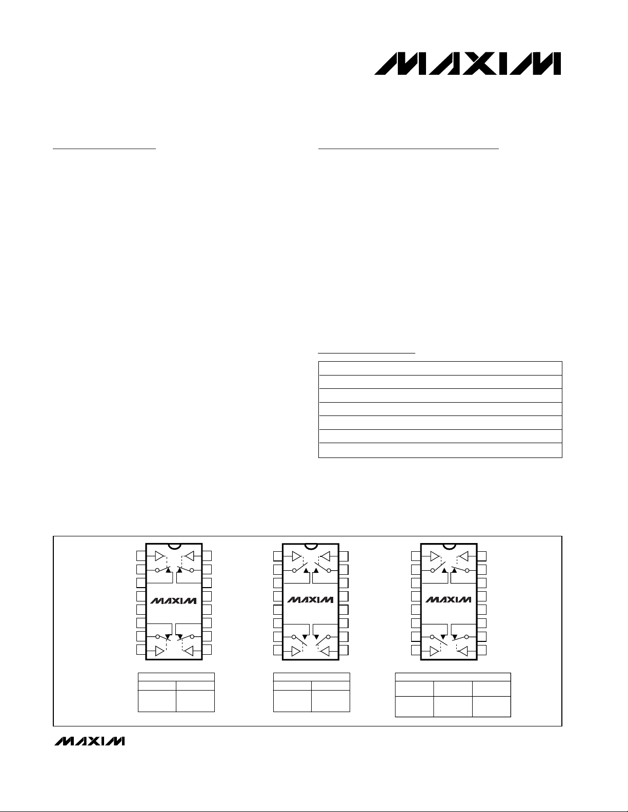
The MAX4677 has four normally closed (NC) switches,
and the MAX4678 has four normally open (NO) switches. The MAX4679 has two NC and two NO switches
and features guaranteed break-before-make switching.
The MAX4677/MAX4678/MAX4679 operate from either
a single +2.7V to +11V or dual ±2.7V to ±5.5V supplies,
making them ideal for use in digital card applications
and single-ended 75Ω systems.
These devices feature a separate logic supply input
that operates from +2.7V to V+, allowing independent
logic and analog supplies.
________________________Applications
Features
♦ On-Resistance 1.6Ω max
♦ On-Resistance Flatness 0.4Ω max
♦ On-Resistance Matching 0.3Ω max
♦ Dual ±2.7V to ±5.5V or Single +2.7V to +11V
Supply Range
♦ TTL/CMOS-Logic Compatible
♦ Crosstalk -84dB at 1MHz
♦ Off-Isolation -65dB at 1MHz
♦ -3dB Bandwidth: 66MHz
♦ Rail-to-Rail Signal Range
MAX4677/MAX4678/MAX4679
2Ω, Quad, SPST, CMOS Analog Switches
________________________________________________________________ Maxim Integrated Products 1
______________________Pin Configurations/Functional Diagrams/Truth Tables
19-1713; Rev 0; 4/00
For free samples and the latest literature, visit www.maxim-ic.com or phone 1-800-998-8800.
For small orders, phone 1-800-835-8769.
Ordering Information
Rail-to-Rail is a registered trademark of Nippon Motorola, Ltd.
Reed Relay Replacement
Test Equipment
Communications Systems
Audio Signal Routing
Avionics
ADC Systems
Data-Acquisition Systems
PBX/PABX Systems
PART TEMP. RANGE PIN-PACKAGE
MAX4677EUE -40°C to +85°C 16 TSSOP
MAX4677EPE -40°C to +85°C 16 DIP
MAX4678EUE -40°C to +85°C 16 TSSOP
MAX4678EPE -40°C to +85°C 16 DIP
MAX4679EUE -40°C to +85°C 16 TSSOP
MAX4679EPE -40°C to +85°C 16 DIP
TOP VIEW
IN1
COM1
NC1
GND
NC4
COM4
IN4
1
2
3
V-
4
5
6
7
8
LOGIC SWITCH
MAX4677
DIP/TSSOP
MAX4677
0
1
ON
OFF
16
IN2
COM2
15
NC2
14
13
V+
VL
12
11
NC3
10
COM3
9
IN3
1
IN1
2
COM1
3
NO1
V-
4
MAX4678
5
GND
6
NO4
7
COM4
8
IN4
DIP/TSSOP
MAX4678
LOGIC SWITCH
0
1
SWITCHES SHOWN FOR LOGIC "0" INPUT
OFF
ON
16
IN2
15
COM2
14
NO2
13
V+
12
VL
11
NO3
10
COM3
9
IN3
IN1
COM1
NO1
GND
NO4
COM4
IN4
V-
1
2
3
4
5
6
7
8
LOGIC
0
1
MAX4679
DIP/TSSOP
MAX4679
SWITCHES
1, 4
OFF
ON
16
IN2
15
COM2
14
NC2
13
V+
12
VL
11
NC3
10
COM3
9
IN3
SWITCHES
2, 3
ON
OFF
Page 2
MAX4677/MAX4678/MAX4679
2Ω, Quad, SPST, CMOS Analog Switches
2 _______________________________________________________________________________________
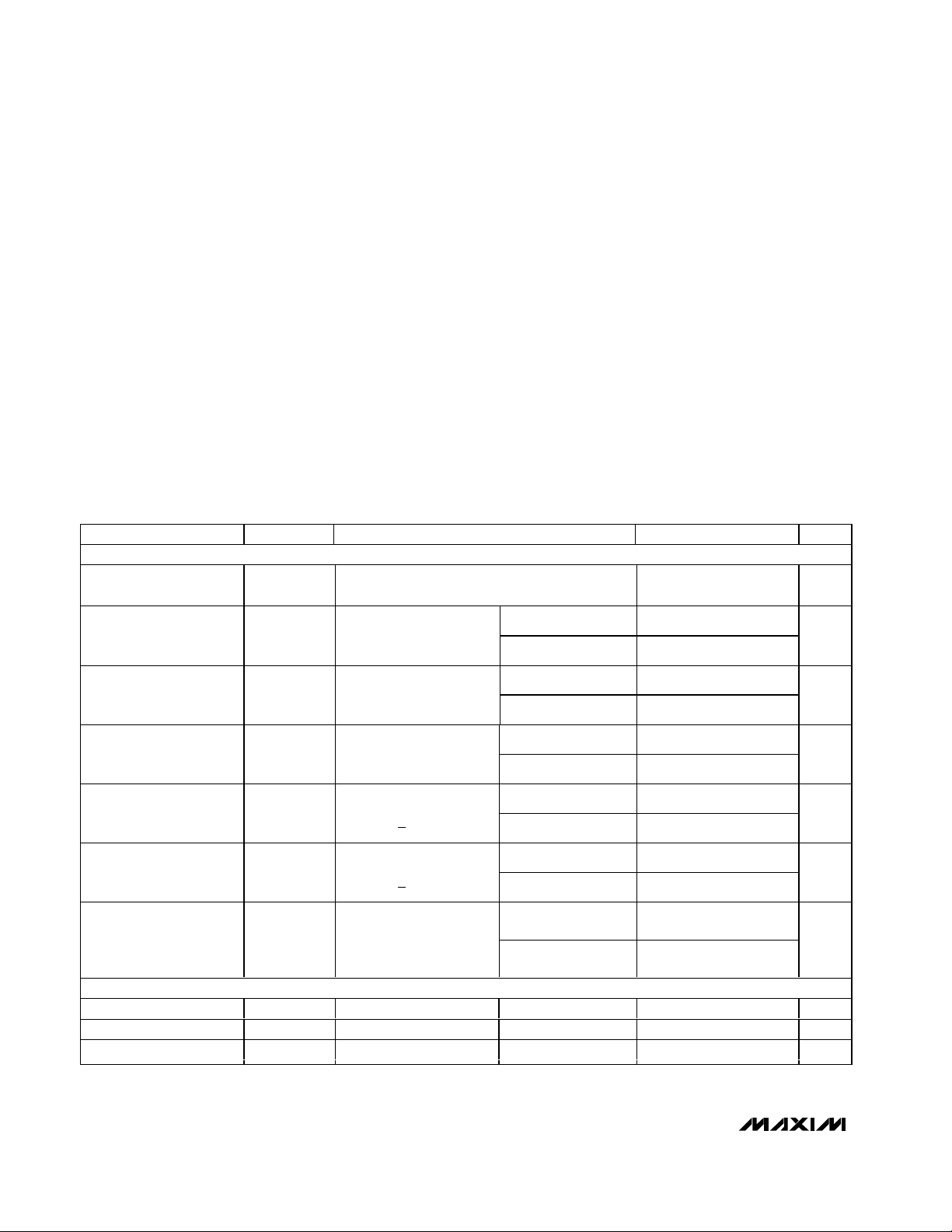
ABSOLUTE MAXIMUM RATINGS
ELECTRICAL CHARACTERISTICS–Dual Supplies
(V+ = +5V ±10%, V- = -5V ±10%, VL= +2.7V to V+, GND = 0, VIH= +2.4V, VIL= +0.8V, TA= T
MIN
to T
MAX
, unless otherwise noted.
Typical values are at T
A
= +25°C.) (Note 2)
Stresses beyond those listed under “Absolute Maximum Ratings” may cause permanent damage to the device. These are stress ratings only, and functional
operation of the device at these or any other conditions beyond those indicated in the operational sections of the specifications is not implied. Exposure to
absolute maximum rating conditions for extended periods may affect device reliability.
V+ to GND ..............................................................-0.3V to +12V
V- to GND ...............................................................+0.3V to -12V
V+ to V- ................................................................................+12V
V
L
, IN_ to GND (Note 1) ...............................-0.3V to (V+ + 0.3V)
V
COM_
,
V
NC_
,
V
NO_
(Note 1)............................................V- to V+
Current (any terminal).......................................................±50mA
Continuous Current (COM_, NC_, NO_).........................±100mA
Peak Current (COM_, NC_, NO_
pulsed at 1ms 10% duty cycle) .................................±200mA
Continuous Power Dissipation (T
A
= +70°C)
16-Pin Plastic DIP (derate 10.5mW/°C above +70°C)..842mW
16-Pin TSSOP (derate 5.7mW/°C above +70°C)..........457mW
Operating Temperature Range ...........................-40°C to +85°C
Storage Temperature Range .............................-65°C to +150°C
Junction Temperature......................................................+150°C
Lead Temperature (soldering, 10s) .................................+300°C
)
)
Note 1: Signals on NC_, NO_, COM_, or IN_ exceeding V+ or V- are clamped by internal diodes. Limit forward diode current to
maximum current rating.
PARAMETER SYMBOL CONDITIONS MIN TYP MAX UNITS
ANALOG SWITCH
Input Voltage Range
On-Resistance R
On-Resistance Match
Between Channels
(Note 3)
On-Resistance Flatness
(Note 4)
NC_ or NO_ Off-Leakage
Current (Note 5)
COM_ Off-Leakage
Current (Note 5)
COM_ On-Leakage
Current (Note 5)
LOGIC INPUT
Input Logic High V
Input Logic Low V
Input Leakage Current I
V
COM
_, VNC_
V
NO
ON
∆R
ON
R
FLAT
I
N_(OFF)
ICOM_(OFF
I
COM_(ON
IH
IL
IN
_,
V+ = 4.5V, V- = -4.5V,
_ = 50mA,
I
COM
V
_ or VNC_ = ±3.3V
NO
V+ = 4.5V, V- = -4.5V,
I
_ = 50mA, VNO_ or
COM
_ = ±3.3V
V
NC
V+ = 4.5V, V- = -4.5V,
I
_ = 50mA, VNO_ or
COM
_ = ±3.3V, 0
V
NC
V+ = +5.5V, V- = -5.5V,
_ or VNC_ = ±4.5V,
V
NO
V
_ = +4.5V
COM
V+ = +5.5V, V- = -5.5V,
V
_ or VNC_ = ±4.5V,
NO
_ = +4.5V
V
COM
V+ = +5.5V, V- = -5.5V,
V
= ±4.5V,
COM_
_ or VNC_ = ±4.5V or
V
NO
floating
T
= +25°C 1.2 1.6
A
= T
T
A
T
A
T
A
T
A
T
A
T
A
T
A
T
A
T
A
T
A
T
A
to T
MIN
MIN
MIN
MIN
MIN
MIN
to T
to T
to T
to T
to T
MAX
MAX
MAX
MAX
MAX
MAX
= +25°C 0.2 0.3
= T
= +25°C 0.2 0.4
= T
= +25°C -1 0.1 1
= T
= +25°C -1 0.1 1
= T
= +25°C -2 0.2 2
= T
VL = V+ 2.4 V
VL = V+ 0.8 V
VL = V+ -1 0.005 1 µA
V- V+ V
2
0.5
0.5
-10 10
-10 10
-25 25
Ω
Ω
Ω
nA
nA
nA
Page 3
MAX4677/MAX4678/MAX4679
2Ω, Quad, SPST, CMOS Analog Switches
_______________________________________________________________________________________ 3
ELECTRICAL CHARACTERISTICS–Dual Supplies (continued)
(V+ = +5V ±10%, V- = -5V ±10%, VL= +2.7V to V+, GND = 0, VIH= +2.4V, VIL= +0.8V, TA= T
MIN
to T
MAX
, unless otherwise noted.
Typical values are at T
A
= +25°C.) (Note 2)
(
)
PARAMETER SYMBOL CONDITIONS MIN TYP MAX UNITS
POWER SUPPLY
Positive Supply Voltage V+ +2.7 +5.5 V
Negative Supply Voltage V- -2.7 -5.5 V
Logic Supply Voltage V
Positive Supply Current I+ IN_ = GND or V
Negative Supply Current I-
Logic Supply Current I
Ground Current I
L
L
GND
L
IN_ = GND or V
IN_ = GND or V
L
L
IN_ = 0 or V+, V+ = 5.5V, V- = -5.5V 1 µA
DYNAMIC
Turn-On Time t
Turn-Off Time t
Break-Before-Make Delay t
ON
OFF
BBM
Charge Injection Q R
Off-Isolation V
ISO
Crosstalk R
-3dB Bandwidth BW R
NC or NO OffCapacitance
COM Off-Capacitance C
On-Capacitance C
C
(N_OFF)
COMOFF
(ON)
V+ = +4.5V, V- = -4.5V,
or VNO_= ±3.3V,
V
NC_
V
= V+, Figure 2
L
V+ = +4.5V, V- = -4.5V,
or VNO_ = ±3.3V,
V
NC_
= V+, Figure 2
V
L
Figure 3, MAX4679 only, R
C
= 35pF
L
= 0, C
GEN
R
= 50Ω, C
L
= 50Ω, C
L
= 50Ω, R
S
= 1nF, V
L
= 5pF, f = 1MHz, Figure 5a -65 dB
L
= 5pF, f = 1MHz, Figure 6a -84 dB
L
= 50Ω, Figure 7a 66 MHz
L
f = 1MHz, Figure 8 85 pF
f = 1MHz, Figure 8 85 pF
f = 1MHz, Figure 8 350 pF
T
= +25°C 200 350
A
= T
T
A
T
A
T
A
= 300Ω,
L
= 0, Figure 4 85 pC
GEN
to T
MIN
MIN
to T
MAX
MAX
= +25°C 110 150
= T
2.7 V+ V
0.001 1 µA
-1 µA
1 µA
500
350
5ns
ns
ns
Page 4
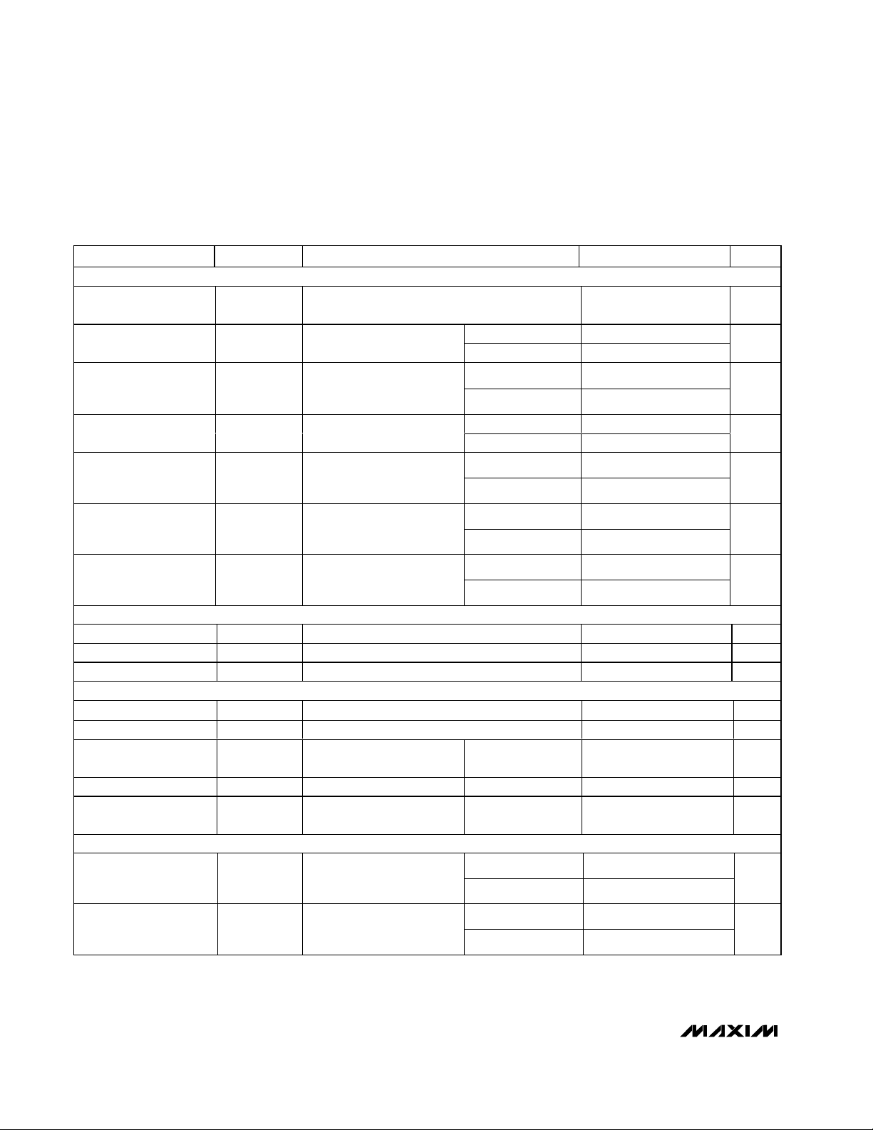
MAX4677/MAX4678/MAX4679
2Ω, Quad, SPST, CMOS Analog Switches
4 _______________________________________________________________________________________
ELECTRICAL CHARACTERISTICS–Single Supply
(V+ = +5V ±10%, V- = 0, VL= +2.7V to V+, GND = 0, VIH= +2.4V, VIL= +0.8V, TA= T
MIN
to T
MAX
, unless otherwise noted. Typical
values are at T
A
= +25°C.) (Note 2)
)
PARAMETER SYMBOL CONDITIONS MIN TYP MAX UNITS
ANALOG SWITCH
V
_,
Input Voltage Range
On-Resistance R
On-Resistance Match
Between Channels
(Note 3)
On-Resistance Flatness
(Note 4)
NC_ or NO_ OffLeakage Current
(Note 5)
COM_ Off-Leakage
Current (Note 5)
COM_ On-Leakage
Current (Note 5)
COM
_, VNC_
V
NO
ON
∆R
ON
R
FLAT
N_(OFF)
I
I
COM_(OFF
I
COM_(ON)
V+ = +4.5V, I
_ or VNC_ = 3.3V
V
NO
V+ = +4.5V, I
_ or VNC_ = 3.3V
V
NO
V+ = +4.5V, I
_ or VNC_ = 3.3V, 1.5V
V
NO
COM
COM
COM
V+ = +5.5V;
_ or VNC_ = 4.5V, 1V;
V
NO
V
_ = 1V, 4.5V
COM
V+ = +5.5V;
_ or VNC_ = 4.5V, 1V;
V
NO
V
_ = 1V, 4.5V
COM
V+ = +5.5V; V
4.5V; V
COM
_ or VNC_ = 1V,
NO
4.5V, or floating
_ = 50mA,
_ = 50mA,
_ = 50mA,
_ = 1V,
T
= +25°C 1.8 2.7
A
T
= T
A
T
A
T
A
T
A
T
A
T
A
T
A
T
A
T
A
T
A
T
A
to T
MIN
= +25°C 0.05 0.15
= T
to T
MIN
= +25°C 0.15 0.25
= T
to T
MIN
= +25°C -1 0.1 1
= T
to T
MIN
= +25°C -1 0.1 1
= T
to T
MIN
= +25°C -2 0.2 2
= T
to T
MIN
LOGIC INPUT
Input Low Voltage V
Input High Voltage V
Input Leakage Current I
IL
IH
IN
VL = V+ 0.8 V
VL = V+ 2.4 V
VL = V+ -1 0.005 1 µA
POWER SUPPLY
Positive Supply Voltage V+ 2.7 6 V
Logic Supply Voltage V
L
MAX
MAX
MAX
MAX
MAX
MAX
0V+V
-10 10
-10 10
-25 25
2.7 V+ V
3.5
0.3
0.4
Ω
Ω
Ω
nA
nA
nA
Positive Supply Current l+ V
Logic Supply Current I
Ground Current I
L
GND
= 0 or V
IN_
V
= 0 or VL, V+ = 5.5V 1 µA
IN_
V
= 0 or V
IN_
= V+ 1 1 µA
L, VL
V+ = 5.5V 1 10 µA
L,
DYNAMIC
Turn-On Time t
Turn-Off Time t
ON
OFF
VL = V+, V+ = +4.5V; VNC_
or V
C
= 3.3V, R
NO_
= 35pF, Figure 2
L
= 300Ω,
L
VL = V+, V+ = +4.5V; VNC_
or V
C
= 3.3V, R
NO_
= 35pF, Figure 2
L
= 300Ω,
L
T
= +25°C 600 1000
A
T
= T
A
T
A
T
A
to T
MIN
MIN
to T
MAX
MAX
= +25°C 120 165
= T
1400
ns
ns
400
Page 5

MAX4677/MAX4678/MAX4679
2Ω, Quad, SPST, CMOS Analog Switches
_______________________________________________________________________________________ 5
ELECTRICAL CHARACTERISTICS–Single Supply (continued)
(V+ = +5V ±10%, V- = 0, VL= +2.7V to V+, GND = 0, VIH= +2.4V, VIL= +0.8V, TA= T
MIN
to T
MAX
, unless otherwise noted. Typical
values are at T
A
= +25°C.) (Note 2)
(
)
Typical Operating Characteristics
(TA = +25°C, unless otherwise noted.)
0
0.6
0.4
0.2
0.8
1.0
1.2
1.4
1.6
1.8
2.0
-5 -1-3 135
MAX4677/8/9-01
V
COM
(V)
R
ON
(Ω)
ON-RESISTANCE vs. V
COM
(DUAL SUPPLY)
V± = ±2.5V
V± = ±3V
V± = ±4V
V± = ±5V
0
1.5
1.0
0.5
2.0
2.5
3.0
3.5
4.0
4.5
5.0
021 345
MAX4677/8/9-02
V
COM
(V)
R
ON
(Ω)
ON-RESISTANCE vs. V
COM
(SINGLE SUPPLY)
V- = 0
V+ = 3V
V+ = 5V
V+ = 9V
V+ = 12V
V+ = 2.5V
V+ = 4V
TA = +85°C
TA = +25°C
TA = -40°C
0
0.4
0.2
0.8
0.6
1.2
1.0
1.4
-5 -1-3 1 3-4 0-2 2 4 5
ON-RESISTANCE vs. V
COM
AND
TEMPERATURE (DUAL SUPPLIES)
MAX4677/8/9-03
V
COM
(V)
R
ON
(Ω)
V+ = +5V
V- = -5V
VL = V+
Note 2: The algebraic convention, where the most negative value is a minimum and the most positive value a maximum, is used
in this data sheet.
Note 3: ∆R
ON = RON(MAX) - RON(MIN).
Note 4: Flatness is defined as the difference between the maximum and minimum value of on-resistance as measured over the
specified analog signal ranges.
Note 5: Leakage parameters are 100% tested at maximum-rated hot operating temperature and the highest supply voltage, and
guaranteed by correlation at +25°C.
PARAMETER SYMBOL CONDITIONS MIN TYP MAX UNITS
Break-Before- Make
Delay
Charge Injection Q R
Off-Isolation V
t
BBM
ISO
MAX4679 only, R
= 0, C
GEN
= 50Ω, C
R
L
= 1nF, V
L
= 5pF, f = 1MHz, Figure 5b -65 dB
L
= 300Ω, CL = 35pF, Figure 3 5 ns
L
= 0, Figure 4 9 pC
GEN
Crosstalk RL = 50Ω, CL= 5pF, f = 1MHz, Figure 6b -84 dB
-3dB Bandwidth BW R
NC or NO OffCapacitance
COM Off-Capacitance C
On-Capacitance C
C
(N_OFF)
COMOFF
(ON)
= 50Ω, R
S
= 50Ω, Figure 7b 63 MHz
L
f = 1MHz, Figure 8 85 pF
f = 1MHz, Figure 8 85 pF
f = 1MHz, Figure 8 350 pF
Page 6

MAX4677/MAX4678/MAX4679
2Ω, Quad, SPST, CMOS Analog Switches
6 _______________________________________________________________________________________
Typical Operating Characteristics (continued)
(TA= +25°C, unless otherwise noted.)
-40
40 60
0-20 20
80
POWER-SUPPLY CURRENT
vs. TEMPERATURE
MAX46778/9-11
TEMPERATURE °(C)
0.00001
0.001
0.1
100
1000
10
1
0.01
0.0001
I+, I-
I
L
I+, I-, I
L
(nA)
0
0.5
1.0
1.5
2.0
2.5
0 2.0 2.51.0 1.50.5 3.0 3.5 4.0 4.5 5.0
ON-RESISTANCE vs. V
COM
AND
TEMPERATURE (SINGLE SUPPLY)
AMX4677/8/9-04
V
COM
(V)
R
ON
(Ω)
TA = +85°C
TA = +25°C
TA = -40°C
V+ = +5V
V- = 0
VL = V+
0.000001
0.0001
0.00001
0.01
0.001
0.1
1
-40 0-20 20 40 60 80
ON-/OFF-LEAKAGE CURRENT
vs. TEMPERATURE
MAX4677/8/9-05
TEMPERATURE (°C)
LEAKAGE CURRENT (nA)
ON-LEAKAGE
OFF-LEAKAGE
0
20
10
40
30
60
50
70
90
80
100
-5 -3 -2 -1-4 012 435
CHARGE INJECTION
vs. V
COM
MAX4677/8/9-06
V
COM
(V)
CHARGE (pC)
VL = V+
V+ = +5V
V- = -5V
V+ = +5V
V- = 0
75
175
125
275
225
425
375
325
475
±1.5
±2.5±2.0 ±3.0 ±3.5 ±4.0 ±4.5
tON, t
OFF
vs. SUPPLY VOLTAGE
(DUAL SUPPLIES)
MAX4677/8/9-07
V+, V- (V)
TIME (ns)
t
ON
t
OFF
VL = V+
±5.0
75
115
95
175
155
135
235
215
195
255
-40 0 20-20 40 60 80 100
tON, t
OFF
vs. TEMPERATURE
MAX4677/8/9-08
TEMPERATURE (°C)
TIME (ns)
t
ON
t
OFF
V+ = +5V
V- = -5V
V
L
= V+
75
125
225
175
275
325
1.5 2.52.0 3.0 3.5 4.0 4.5 5.0
tON, t
OFF
vs. LOGIC SUPPLY
MAX4677/8/9-09
VL (V)
TIME (ns)
t
ON
t
OFF
V+ = +5V
V- = -5V
INPUT THRESHOLD vs. LOGIC SUPPLY
2.5
V+ = +5V
V- = -5V
2.0
1.5
1.0
THRESHOLD VOLTAGE (V)
0.5
0
1.5 2.5 3.02.0 3.5 4.0 4.5 5.0 5.5
V
TH (RISING)
VL (V)
V
TH (FALLING)
MAX4677/8/9-10
Page 7

MAX4677/MAX4678/MAX4679
2Ω, Quad, SPST, CMOS Analog Switches
_______________________________________________________________________________________ 7
Typical Operating Characteristics (continued)
(TA= +25°C, unless otherwise noted.)
0
-90
0.1 100101
INSERTION LOSS,
OFF-ISOLATION, AND CROSSTALK
vs. FREQUENCY (DUAL SUPPLIES)
-60
-80
-20
-40
10
-50
-70
-10
-30
MAX4677/8/9-12
(MHz)
(dB)
1. -3dB, 66MHz
2. -65dB, 1MHz
3. -84dB,1MHz
CROSSTALK
OFF-ISOLATION
INSERTION LOSS
1
2
3
V+ = +5V
V- = -5V
V
L
= V+
0
-90
0.1 100101
-60
-80
-20
-40
10
-50
-70
-10
-30
MAX4677/8/9-13
(MHz)
(dB)
INSERTION LOSS,
OFF-ISOLATION, AND CROSSTALK
vs. FREQUENCY (SINGLE SUPPLY)
1. -3dB, 63MHz
2. -65dB, 1MHz
3. -84dB,1MHz
CROSSTALK
OFF-ISOLATION
INSERTION LOSS
1
2
3
V+ = +5V
V- = -5V
V
L
= V+
Pin Description
PIN
MAX4677 MAX4678 MAX4679 NAME FUNCTION
1, 8, 9, 16 1, 8, 9, 16 1, 8, 9, 16
2, 7, 10, 15 2, 7, 10, 15 2, 7, 10, 15
3, 6, 11, 14 ——
— 3, 6, 11, 14 —
——3, 6 NO1, NO4 Analog Switch Normally Open Terminals
——11, 14 NC2, NC3 Analog Switch Normally Closed Terminals
444 V-
5 5 5 GND Ground
12 12 12 V
13 13 13 V+ Positive Supply Input
IN1, IN2,
IN3, IN4
COM1, COM2,
COM3, COM4
NC1, NC2,
NC3, NC4
NO1, NO2,
NO3, NO4
L
Logic Inputs
Analog Switch Common Terminals
Analog Switch Normally Closed Terminals
Analog Switch Normally Open Terminals
Negative Supply-Voltage Input. Connect to GND
for single-supply operation.
Logic Supply Input
Page 8

MAX4677/MAX4678/MAX4679
2Ω, Quad, SPST, CMOS Analog Switches
8 _______________________________________________________________________________________
___________Applications Information
Overvoltage Protection
Proper power-supply sequencing is recommended for
all CMOS devices. Do not exceed the absolute maximum ratings because stresses beyond the listed ratings
can cause permanent damage to the devices. Always
sequence V+ on first, then V-, then VLfollowed by the
logic inputs, NO_, NC_, or COM. If proper power-supply
sequencing is not possible, add two small signal diodes
(D1, D2) in series with the supply pins, and a Schottky
diode between V+ and VLfor overvoltage protection
(Figure 1). Adding diodes reduces the analog signal
range to one diode drop below V+ and one diode drop
above V-, but does not affect the devices’ low switch
resistance and low leakage characteristics. Device operation is unchanged, and the difference between V+ and
V- should not exceed 11V.
Power-supply bypassing improves noise margin and
prevents switching noise from propagating from the V+
supply to other components. A 0.1µF capacitor connected from V+ to GND is adequate for most applications.
Figure 1. Overvoltage Protection Using External Blocking Diodes
Figure 2. Switching Time
Figure 3. Break-Before-Make Interval (MAX4679 Only)
MAX4677
MAX4678
MAX4679
SWITCH
V
COM
INPUT
LOGIC
INPUT
V+
V
COM_
IN_
GND
0V
C
INCLUDES FIXTURE AND STRAY CAPACITANCE.
L
V
= V
OUT
COM (
RL + R
V+
R
L
300Ω
SWITCH
OUTPUT
C
L
35pF
V
OUT
V+
L
R
OR NC_
V-
V-
L
ON
NO_
)
*INTERNAL PROTECTION DIODES
LOGIC
INPUT
SWITCH
OUTPUT
V
2
+3V
MAX4677
MAX4678
MAX4679
COM_
0
0
V+
D1
V
*
*
D2
V-
50%
V
OUT
0.9 x V
0UT
t
ON
*
*
tr < 20ns
tf < 20ns
t
OFF
0.9 x V
OUT
L
NO_
MAX4679
V
COM1
V
COM2
LOGIC
INPUT
V+
V
= +3V
= +3V
COM1
COM2
I
N1
I
N2
GND
C
INCLUDES FIXTURE AND STRAY CAPACITANCE.
L
V+
V+
L
NO1
NC2
V-
V-
V
OUT2
R
C
L2
L2
RL = 300Ω
= 35pF
C
L
V
OUT1
R
C
L1
L1
LOGIC
INPUT
SWITCH
OUTPUT 1
(V
SWITCH
OUTPUT 2
(V
OUT1
OUT2
+3V
50%
0
0.9 x V
0
)
)
0
t
D
0UT1
0.9 x V
OUT2
t
D
Page 9

MAX4677/MAX4678/MAX4679
2Ω, Quad, SPST, CMOS Analog Switches
_______________________________________________________________________________________ 9
Figure 4. Charge Injection
Figure 5a. Off-Isolation Test Circuit, Dual Supplies
Figure 5b. Off-Isolation Test Circuit, Single Supply
MAX4677
MAX4678
MAX4679
R
GEN
V
GEN
NETWORK
ANALYZER
PORT 1
50Ω
PORT 2
-5V
N_1
N_ _
COM_
GND
V-
V+
V
L
V+
V+
NC_OR
NO_
V-
IN
V-
= +3V
V
IN
COM1
IN_
MAX4677
MAX4678
MAX4679
IN1
V
OUT
C
L
V
OUT
IN
IN
NETWORK
ANALYZER
PORT 1
OFF
OFF
IN DEPENDS ON SWITCH CONFIGURATION;
INPUT POLARITY DETERMINED BY SENSE OF SWITCH.
50Ω
Q = (∆V
N_1
ON
ON
OUT
MAX4677
MAX4678
)(CL)
∆V
OUT
OFF
OFF
COM1
IN_
MAX4679
GND
COM_
V
V+
L
+5V
PORT 2
N_ _
V- GND
COM_
V
V+
L
+5V
Page 10

MAX4677/MAX4678/MAX4679
2Ω, Quad, SPST, CMOS Analog Switches
10 ______________________________________________________________________________________
Figure 7a. Insertion Loss Test Circuit, Dual Supplies
Figure 6b. Crosstalk Test Circuit, Single Supply
Figure 6a. Crosstalk Test Circuit, Dual Supplies
NETWORK
NETWORK
ANALYZER
PORT 1
PORT 2
COM1
COM_
MAX4677
MAX4678
MAX4679
N_1
IN1
N_ _
IN2
ANALYZER
PORT 1
V+
50Ω
PORT 2
COM1
COM_
MAX4677
MAX4678
MAX4679
N_1
IN1
N_ _
IN2
V+
50Ω
V+
GNDV-
V-
NETWORK ANALYZER
L
PORT 1
PORT 2
V+V
V+
COM1
COM_
V-
GND
-5V +5V
MAX4677
MAX4678
MAX4679
GND
V+
V
L
V+
V-
N_1
V
V+
L
V+
Page 11

MAX4677/MAX4678/MAX4679
2Ω, Quad, SPST, CMOS Analog Switches
______________________________________________________________________________________ 11
Figure 7b. Insertion Loss Test Circuit, Single Supply
Chip Information
TRANSISTOR COUNT: 240
PROCESS: CMOS
NETWORK ANALYZER
PORT 1
PORT 2
COM1
V-
MAX4677
MAX4678
MAX4679
GND
N_1
IN_
V
V+
L
V+
+5V
Page 12

MAX4677/MAX4678/MAX4679
2Ω, Quad, SPST, CMOS Analog Switches
Maxim cannot assume responsibility for use of any circuitry other than circuitry entirely embodied in a Maxim product. No circuit patent licenses are
implied. Maxim reserves the right to change the circuitry and specifications without notice at any time.
12 ____________________Maxim Integrated Products, 120 San Gabriel Drive, Sunnyvale, CA 94086 408-737-7600
© 2000 Maxim Integrated Products Printed USA is a registered trademark of Maxim Integrated Products.
Package Information
TSSOP.EPS
PDIPN.EPS
 Loading...