

Page 1
________________General Description
The MAX4675/MAX4676 single analog switches feature
3Ω (max) on-resistance (RON) and 0.7Ω flatness when
operating from dual ±5V supplies. These switches can
handle Rail-to-Rail®analog signals. Off-leakage current
is 0.1nA at TA= +25°C. The MAX4675/MAX4676 are
ideal in low-distortion applications and are the preferred solution over mechanical relays in automated
test equipment or applications where current switching
is required. They are more reliable than mechanical
relays, have low power requirements (<1µA), and are
available in a space-saving 6-pin SOT23 package.
The MAX4675 has a single normally open (NO) switch,
and the MAX4676 has a single normally closed (NC)
switch.
The MAX4675/MAX4676 operate from either a single
+2.7V to +5.5V or dual ±2.7V to ±5.5V supplies, making them ideal for use in digital card applications and
single-ended 75Ω systems.
________________________Applications
Reed Relay Replacement
Test Equipment
Communications Systems
PBX, PABX Systems
Audio Signal Routing
Avionics
ADC Systems
Data-Acquisition Systems
____________________________Features
♦ 3Ω (max) R
ON
♦ 0.7Ω (max) RONFlatness
♦ Dual ±2.7V to ±5.5V or Single +2.7V to +5.5V
Supply Range
♦ Off-Isolation
-75dB at 1MHz, Dual Supply
-65dB at 1MHz, Single Supply
♦ -3dB Bandwidth 250MHz
♦ Rail-to-Rail Signal Handling
MAX4675/MAX4676
3Ω Single SPST Analog Switches
________________________________________________________________ Maxim Integrated Products 1
19-1747; Rev 0; 7/00
For free samples and the latest literature, visit www.maxim-ic.com or phone 1-800-998-8800.
For small orders, phone 1-800-835-8769.
_______________Ordering Information
Rail-to-Rail is a registered trademark of Nippon Motorola, Ltd.
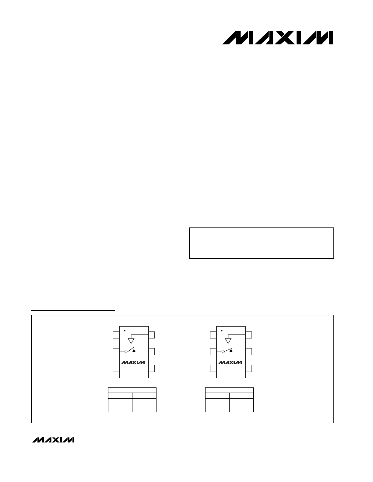
Pin Configurations/Functional Diagrams/Truth Tables
PART
MAX4675EUT-T
MAX4676EUT-T
TEMP.
RANGE
-40°C to +85°C 6 SOT23-6 AAND
-40°C to +85°C 6 SOT23-6 AANE
PINPACKAGE
SOT
MARK
TOP VIEW
16IN
V+
COM
2
MAX4675
34
SOT23
MAX4675
IN SWITCH
0
1
5 NO
GNDV-
OFF
ON
16IN
V+
COM
2
MAX4676
34
SOT23
MAX4676
IN SWITCH
0
1
5 NC
GNDV-
ON
OFF
Page 2
MAX4675/MAX4676
3Ω Single SPST Analog Switches
2 _______________________________________________________________________________________
ABSOLUTE MAXIMUM RATINGS
ELECTRICAL CHARACTERISTICS—DUAL SUPPLIES
(V+ = +5V ±10%, V- = -5V ±10%, GND = 0, VIH= +2.4V, VIL= 0.8V, TA= T
MIN
to T
MAX
, unless otherwise noted. Typical values are
at T
A
= +25°C.) (Notes 2, 3)
Stresses beyond those listed under “Absolute Maximum Ratings” may cause permanent damage to the device. These are stress ratings only, and functional
operation of the device at these or any other conditions beyond those indicated in the operational sections of the specifications is not implied. Exposure to
absolute maximum rating conditions for extended periods may affect device reliability.
V+ to GND ................................................................-0.3V to +6V
V- to GND .................................................................+0.3V to -6V
V+ to V- ..................................................................................12V
IN to GND .....................................................-0.3V to (V+ + 0.3V)
All Other Pins (Note 1) ..........................(V- - 0.3V) to (V+ + 0.3V)
Continuous Current (NO, NC, COM) ..............................±100mA
Peak Current (NO, NC, COM, pulsed at 1ms
(10% duty cycle).........................................................±200mA
Continuous Power Dissipation (T
A
= +70°C)
6-Pin SOT23 (derate 8.7mW/°C above +70°C)............691mW
Operating Temperature Range ...........................-40°C to +85°C
Junction Temperature......................................................+150°C
Storage Temperature Range .............................-65°C to +150°C
Lead Temperature (soldering, 10s) .................................+300°C
Note 1: Signals on NO, NC, COM, or IN exceeding V+ or V- will be clamped by internal diodes. Limit forward diode current to maxi-
mum current rating.
,
)
)
)
PARAMETER SYMBOL CONDITIONS MIN TYP MAX UNITS
ANALOG SWITCH
Input Voltage Range
V
,
COM
V
V
NO
NC
V+ = 4.5V, V- = -4.5V, I
On-Resistance R
ON
= 50mA; VNO or V
NC
±3.3V
On-Resistance Flatness
(Note 4)
NC or NO Off-Leakage
Current
R
FLAT
I
N_(OFF
V + = 4.5V , V - = - 4.5V ,
I
C OM
V
N C
= 50m A; V
= ± 3.3V , 0
N O
or
V+ = 5.5V, V- = -5.5V,
V
= 4.5V; VNO or V
COM
±4.5V
V+ = 5.5V, V- = -5.5V,
= +4.5V; VNO or
COM Off-Leakage Current I
COM(OFF
V
V
COM
NC
= ±4.5V
V+ = 5.5V, V- = -5.5V,
COM On-Leakage Current I
COM(ON
V
COM
= ±4.5V; V
NO
or V
= ± 4.5V or floating
LOGIC INPUT
Input Low Voltage V
Input High Voltage V
Input Leakage Current I
IL
IH
IN
DYNAMIC
V+ = +4.5V, V- = -4.5V;
or V
Turn-On Time t
ON
V
NO
R
= 300Ω, C
L
= 3.3V,
NC
= 35p F, Fig ure 2
L
V+ = +4.5V, V- = -4.5V;
Turn-Off Time t
OFF
V
NO
= 300Ω, C
R
L
or V
NC
= 3.3V,
= 35p F, Fig ure 2
L
=
COM
NC
NC
=
T
= +25°C 2.4 3
A
= T
T
A
T
= +25°C 0.4 0.7
A
T
= T
A
T
= +25°C -1 0.1 1
A
= T
T
A
T
= +25°C -1 0.1 1
A
T
= T
A
T
= +25°C -2 0.1 2
A
T
= T
A
T
= +25°C 135 300
A
T
= T
A
T
= +25°C 50 110
A
T
= T
A
to T
MIN
MAX
to T
MIN
MAX
to T
MIN
MAX
to T
MIN
MAX
to T
MIN
MAX
to T
MIN
MAX
to T
MIN
MAX
V- V+ V
4
1.0
-10 10
-10 10
-20 20
0.8 V
2.4 V
-1 0.005 1 µA
375
125
Ω
Ω
nA
nA
nA
ns
ns
Page 3
MAX4675/MAX4676
3Ω Single SPST Analog Switches
_______________________________________________________________________________________ 3
ELECTRICAL CHARACTERISTICS—DUAL SUPPLIES (continued)
(V+ = +5V ±10%, V- = -5V ±10%, GND = 0, VIH= +2.4V, VIL= 0.8V, TA= T
MIN
to T
MAX
, unless otherwise noted. Typical values are
at T
A
= +25°C.) (Notes 2, 3)
ELECTRICAL CHARACTERISTICS—SINGLE SUPPLY
(V+ = +5V ±10%, V- = 0, GND = 0, VIH= +2.4V, VIL= 0.8V, TA= T
MIN
to T
MAX
, unless otherwise noted. Typical values are at
T
A
= +25°C.) (Notes 2, 3)
,
)
)
(
)
(
PARAMETER SYMBOL CONDITIONS MIN TYP MAX UNITS
R
Charge Injection Q
Off-Isolation V
On-Channel Bandwidth
(-3dB)
NC or NO Off-Capacitance C
COM Off-Capacitance C
On-Capacitance C
BW R
N_OFF
C OM OFF)
(ON)
ISO
= 0Ω, C
GEN
V
= 0, Figure 3
GEN
R
= 50Ω, C
L
f = 1MHz, Figure 4
= 50Ω, R
S
f = 1MHz, Figure 5 T
f = 1MHz, Figure 5 T
f = 1MHz, Figure 5 T
= 1nF,
L
= 5pF,
L
= 50Ω 250 MHz
L
POWER SUPPLY
Supply Voltage V+, V- ±2.7 ±5.5 V
V
= 0 or 5.5V, V+ =
Positive Supply Current I+
Negative Supply Current I-
IN
5.5V, V- = -5.5V
V
= 0 or 5.5V,
IN
V+ = 5.5V, V- = -5.5V
T
= +25°C87pC
A
= +25°C -75 dB
T
A
= +25°C85pF
A
= +25°C85pF
A
= +25°C 350 pF
A
T
= +25°C 0.002 1
A
T
= T
A
T
= +25°C -1 -0.002
A
= T
T
A
to T
MIN
MAX
MIN
to T
MAX
-10
10
µA
µA
PARAMETER SYMBOL CONDITIONS MIN TYP MAX UNITS
ANALOG SWITCH
V
,
Input Voltage Range
On-Resistance R
On-Resistance Flatness
(Note 4)
NC or NO Off-Leakage
Current
COM Off-Leakage Current I
COM
V
V
NO
ON
R
FLAT
I
N_(OFF
COM(OFF
NC
V + = 4.5V ; I
V
NO
V + = 4.5V ; I
V
or V
N O
3.3V
V+ = 5.5V; VNO or
= 4.5V or 0;
V
NC
V
COM
V+ = 5.5V; V
V
= 4.5V or 0;
NC
V
COM
= 50m A;
C OM
or VNC = 3.3V
= 50m A;
C OM
= 1.5V , 2.5V ,
N C
= 0 or 4.5V
or
NO
= 0 or 4.5V
T
= +25°C 3.5 5.75
A
= T
T
A
T
= +25°C 0.4 1.6
A
= T
T
A
T
= +25°C -1 0.1 1
A
T
= T
A
T
= +25°C -1 0.1 1
A
T
= T
A
0 V+ V
MIN
MIN
MIN
MIN
to T
to T
to T
to T
MAX
MAX
-10 10
MAX
-10 10
MAX
7.5
2
Ω
Ω
nA
nA
Page 4

MAX4675/MAX4676
3Ω Single SPST Analog Switches
4 _______________________________________________________________________________________
Note 2: Parameters are 100% tested at +25°C only and guaranteed by correlation through the full-rated temperature range.
Note 3: The algebraic convention, where the most negative value is a minimum and the most positive value a maximum, is used in
this data sheet.
Note 4: Flatness is defined as the difference between the maximum and minimum value of R
ON
as measured over the specified
analog signal ranges.
)
(
)
(
ELECTRICAL CHARACTERISTICS—SINGLE SUPPLY (continued)
(V+ = +5V ±10%, V- = 0, GND = 0, VIH= +2.4V, VIL= 0.8V, TA= T
MIN
to T
MAX
, unless otherwise noted. Typical values are at
T
A
= +25°C.) (Notes 2, 3)
PARAMETER SYMBOL CONDITIONS MIN TYP MAX UNITS
V+ = 5.5V; VNO or
V
= 0, 4.5V,
NC
COM On-Leakage Current I
COM (ON
or floating;
= 0 or 4.5V
V
COM
LOGIC INPUT
Input Low Voltage V
Input High Voltage V
Input Leakage Current I
IL
IH
IN
DYNAMIC
V + = + 4.5V ;
or V
V
Turn-On Time t
ON
NO
R
L
Fi gur e 2
V+ = +4.5V; V
Turn-Off Time t
OFF
Charge Injection Q
Off-Isolation V
On-Channel Bandwidth
(-3dB)
ISO
+3.3V, R
C
L
R
GEN
V
GEN
RL = 50Ω, C
f = 1MHz, Figure 4
R
S
= 300Ω, C
= 35pF, Figure 2
= 50Ω, R
= +3.3V,
NC
= 35p F,
L
NO
= 300Ω,
L
= 0Ω, CL = 1nF,
= 2.5V, Figure 3
= 5pF,
L
= 50Ω 150 MHz
L
or V
NC
T
A
T
A
T
T
T
T
=
T
T
T
T
= +25°C -2 0.2 2
= T
to T
MIN
= +25°C 350 700
A
= T
A
MAX
A
A
MAX
A
A
to
MIN
= +25°C 55 150
= T
to
MIN
= +25°C31pC
= +25°C -65 dB
-20 20
MAX
2.4 V
-1 0.005 1 µA
nA
0.8 V
ns
850
ns
160
NC or NO Off-Capacitance C
COM Off-Capacitance C
On-Capacitance
N_OFF
C OM OFF)
C
(ON)
f = 1MHz, Figure 5 T
f = 1MHz, Figure 5 T
f = 1MHz, Figure 5 T
= +25°C85pF
A
= +25°C85pF
A
= +25°C 350 pF
A
POWER SUPPLY
Supply Voltage V+ 2.7 5.5 V
T
Positive Supply Current I+
V
= 0 or 5V,
IN
V+ = 5.5V
= +25°C 0.002 1
A
= T
T
A
to T
MIN
MAX
10
µA
Page 5
MAX4675/MAX4676
3Ω Single SPST Analog Switches
_______________________________________________________________________________________ 5
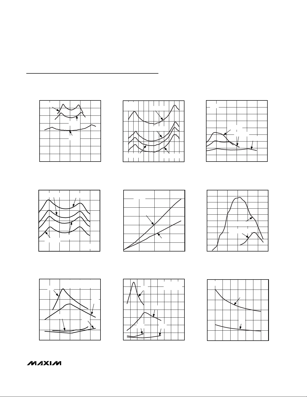
Typical Operating Characteristics
(TA = +25°C, unless otherwise noted.)
0
0.5
1.0
1.5
2.0
2.5
3.0
3.5
4.0
-6 -2-4 0246
ON-RESISTANCE
vs. V
COM
(DUAL SUPPLIES)
MAX4675 toc01
V
COM
(V)
R
ON
(Ω)
V = ±3V
V = ±2.5V
V = ±5V
1.5
1.9
1.7
2.3
2.1
2.5
2.7
-6 -4 -3 -2-5 -1 10 23456
ON-RESISTANCE vs. V
COM
AND TEMPERATURE (DUAL SUPPLIES)
MAX4675 toc02
V
COM
(V)
R
ON
(Ω)
V+ = 5V
V- = -5V
TA = +25°C
TA = +85°C
TA = -40°C
TA = 0°C
0
4
2
10
8
6
16
14
12
18
021 3456
ON-RESISTANCE
vs. V
COM
(SINGLE SUPPLY)
MAX4675 toc03
V
COM
(V)
R
ON
(Ω)
V- = 0
V+ = +2.7V
V+ = +3.3V
V+ = +5V
2.0
3.0
2.5
4.0
3.5
4.5
5.0
0231 456
ON-RESISTANCE vs. V
COM
AND TEMPERATURE (SINGLE SUPPLY)
MAX4675 toc04
V
COM
(V)
R
ON
(Ω)
V+ = +5V
TA = +25°C
TA = +85°C
TA = -40°C
TA = 0°C
0
4
2
8
6
10
12
14
ON/OFF-LEAKAGE CURRENT
vs. TEMPERATURE
MAX4675 toc05
TEMPERATURE (°C)
ON/OFF-LEAKAGE CURRENT (nA)
50 9070 110 130
I
COM(ON)
I
COM(OFF)
V+ = 5V
V- = -5V
0
30
20
10
40
50
60
70
80
90
100
-6 -2-4 0246
CHARGE INJECTION
vs. V
COM
MAX4675 toc06
V
COM
(V)
Q (pC)
DUAL SUPPLIES
SINGLE SUPPLY
0
150
100
50
200
250
300
-6 -2-4 0246
TURN-ON/TURN-OFF TIMES
vs. V
COM
(DUAL SUPPLIES)
MAX4675 toc07
V
COM
(V)
t
ON
, t
OFF
(ns)
A: V+ = +3.5V, V- = -3.5V
B: V+ = +5V, V- = -5V
t
OFFA
t
OFFB
t
ONA
t
ONB
0
200
100
500
400
300
700
600
800
03412 56789
TURN-ON/TURN-OFF TIMES vs. V
COM
(SINGLE SUPPLY)
MAX4675 toc08
V
COM
(V)
t
ON
, t
OFF
(ns)
A: V+ = +5.5V
B: V+ = +3V
t
OFFA
t
OFFB
t
ONA
t
ONB
0
50
100
150
200
250
300
2.0 3.02.5 3.5 4.0 4.5 5.0 5.5 6.0
TURN-ON/TURN-OFF TIMES
vs. SUPPLY VOLTAGE (DUAL SUPPLIES)
MAX4675 toc09
SUPPLY VOLTAGE (V+, V-)
t
ON
, t
OFF
(ns)
V+ = IV-|
t
OFF
t
ON
Page 6

MAX4675/MAX4676
3Ω Single SPST Analog Switches
6 _______________________________________________________________________________________
Typical Operating Characteristics (continued)
(TA= +25°C, unless otherwise noted.)
Pin Description
TURN-ON/TURN-OFF TIMES
vs. SUPPLY VOLTAGE (SINGLE SUPPLY)
MAX4675 toc10
(ns)
OFF
, t
ON
t
140
120
100
2.5
2.0
1.5
(µs)
OFF
, t
ON
t
1.0
0.5
0
2.0 2.5 3.0 3.5 4.0 4.5 5.0 5.5
t
ON
t
OFF
SUPPLY VOLTAGE (V)
V
= V+/2
COM
POWER-SUPPLY CURRENT
vs. TEMPERATURE
10
8
6
4
2
, I- (nA)
0
GND
-2
I+, I
-4
-6
-8
-10
-40 -20 0 20 40 60 80 100
I+
I-
TEMPERATURE (°C)
V+ = +5V
V- = -5V
80
60
40
20
I
GND
TURN-ON/TURN-OFF TIMES
vs. TEMPERATURE (DUAL SUPPLIES)
t
ON
t
OFF
V+ = +5V
0
-40 0 20-20 406080100
TEMPERATURE (°C)
MAX4675 toc13
V- = -5V
10
-10
-30
-50
LOSS (dB)
-70
-90
-110
TURN-ON/TURN-OFF TIMES
vs. TEMPERATURE (SINGLE SUPPLY)
350
300
MAX4675 toc11
250
(ns)
200
OFF
, t
150
ON
t
100
50
0
-40 10 60 110
t
ON
t
OFF
TEMPERATURE (°C)
FREQUENCY RESPONSE
BANDWIDTH
-3dB AT 250MHz
OFF-ISOLATION
-75dB AT 1MHz
0.1
0.01 10 1001 1000
FREQUENCY (MHz)
V+ = +5V
V- = -5V
V+ = +5V
V- = 0
MAX4675 toc14
MAX4675 toc12
PIN
MAX4675 MAX4676
NAME FUNCTION
1 1 V+ Positive Supply
2 2 COM Analog Switch Common Terminals
3 3 V- Negative Supply
4 4 GND Ground
5 — NO Analog Switch Normally Open Terminal
— 5 NC Analog Switch Normally Closed Terminal
6 6 IN Logic Input
Page 7
MAX4675/MAX4676
3Ω Single SPST Analog Switches
_______________________________________________________________________________________ 7
Applications Information
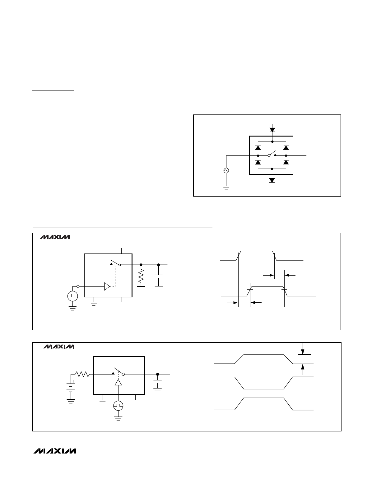
Overvoltage Protection
Proper power-supply sequencing is recommended for all
CMOS devices. Do not exceed the absolute maximum
ratings because stresses beyond the listed ratings can
cause permanent damage to the devices. Always
sequence V+ on first, then V-, followed by the logic
inputs, NO, NC, or COM. If proper power-supply
sequencing is not possible, add two small-signal diodes
(D1, D2) in series with the supply pins (Figure 1). Adding
diodes reduces the analog signal range to one diode
drop below V+ and one diode drop above V- but does
not affect the devices’ low switch resistance and low
leakage characteristics. Device operation is unchanged,
and the difference between V+ and V- should not
exceed 12V.
Power-supply bypassing improves noise margin and
prevents switching noise from propagating from the V+
supply to other components. A 0.1µF capacitor connected from V+ to GND is adequate for most applications.
Figure 1. Overvoltage Protection Using External Blocking
Diodes
Figure 2. Switching Time
Timing Diagrams/Test Circuits
Figure 3. Charge Injection
MAX4675
MAX4676
LOGIC
INPUT
SWITCH
INPUT
NO
OR NC
IN
GND V-
V+
V+
V-
COM
R
L
300Ω
SWITCH
OUTPUT
C
L
35pF
V
OUT
V+
V
g
V-
tr < 20ns
tf < 20ns
t
OFF
0.9 x V
OUT
LOGIC
INPUT
SWITCH
OUTPUT
+3V
0
0
50% 50%
V
OUT
0.9 x V
t
ON
0UT
INCLUDES FIXTURE AND STRAY CAPACITANCE.
C
L
V
= V
OUT
RL + R
MAX4675
MAX4676
R
GEN
V
GEN
COM (
NC
OR NO
GND
R
L
)
ON
V+
V+
COM
V-
IN
V-
= 3.0V
V
IN
V
OUT
C
L
V
OUT
IN
IN
LOGIC INPUT WAVEFORMS INVERTED FOR SWITCHES
THAT HAVE THE OPPOSITE LOGIC SENSE.
∆V
OUT
OFF
OFF
IN DEPENDS ON SWITCH CONFIGURATION;
INPUT POLARITY DETERMINED BY SENSE OF SWITCH.
Q = (∆V
ON
ON
OUT
)(CL)
OFF
OFF
Page 8

MAX4675/MAX4676
3Ω Single SPST Analog Switches
Maxim cannot assume responsibility for use of any circuitry other than circuitry entirely embodied in a Maxim product. No circuit patent licenses are
implied. Maxim reserves the right to change the circuitry and specifications without notice at any time.
8 _____________________Maxim Integrated Products, 120 San Gabriel Drive, Sunnyvale, CA 94086 408-737-7600
© 2000 Maxim Integrated Products Printed USA is a registered trademark of Maxim Integrated Products.
Package Information
Figure 4. Off-Isolation/On-Channel Bandwidth
Figure 5. Channel On/Off-Capacitance
Timing Diagrams/Test Circuits (continued)
V+
SIGNAL
GENERATOR 0dBm
10nF
COM
V+
MAX4675
MAX4676
10nF
V+
MAX4675
MAX4676
V+
COM
IN
ANALYZER
NC
OR NO
GND
V-
V-
0 OR
2.4V
CAPACITANCE
METER
f = 1MHz
NC OR
NO
GND
0 OR
IN
2.4V
V-
V-
6LSOT.EPS
 Loading...