

General Description
The MAX4670 is an integrated T1/E1/J1 analog protection switch for 1+1 and N+1 line-card redundancy
applications. It protects two T1/E1/J1 ports by combining eight SPDT switches in a single package. The
switch is optimized for high-return loss and pulse-template performance in T1/E1/J1 long-haul and short-haul
applications. The part offers built-in chip-side surge
protection capability for short-haul intrabuilding applications.
The MAX4670 replaces two diode arrays or two transient voltage suppressors (TVSs) and four dual-SPDT
relays, significantly reducing board space and simplifying PC board routing. The MAX4670 pinout is targeted
for T1/E1/J1 applications, resulting in a simplified layout
when interfacing with standard line transformers and
line interface units (LIUs).
The MAX4670 has four 1.0Ω (max) on-resistance switches with 60pF/40pF on-/off-capacitances for interfacing to
the LIU transmitter outputs. The MAX4670 also includes
four 10Ω (max) on-resistance switches with low
24pF/12pF on-/off-capacitances for interfacing to the LIU
receiver inputs. Four logic inputs control the receive/
transmit pairs, in addition to a SWITCH input that connects all switches to the system’s protection bus.
The MAX4670 operates from a single +2.7V to +3.6V
supply and is available in 32-pin thermally enhanced
TQFN package. The MAX4670 is specified over the
-40°C to +85°C operating temperature range.
Applications
Optical Multiplexers (ADMs, M13s, etc.)
Edge Routers
Multiservice Switches
Base Station Controllers (Wireless Infrastructure
Equipment)
Media Gateways (VoIP)
Features
♦ Single +3.3V Supply Voltage
♦ Quad-DPDT/Octal-SPDT Switches Support
Two T1/E1/J1 Ports
♦ Low R
ON
♦ 0.7Ω (typ) in Transmit Path; 5Ω (typ) in
Receive Path
♦ Low CON/C
OFF
60pF/40pF (typ) in Transmit Path
24pF/12pF (typ) in Receive Path
♦ Chip Surge Protection
IEC 61000-4-5 (8µs to 20µs Surge)
Class 2 (±1kV)
♦ -70dB (typ) Crosstalk/Off-Isolation (3MHz)
♦ Small, 32-Pin TQFN Package
MAX4670
Integrated T1/E1/J1 Short-Haul and
Long-Haul Protection Switch
________________________________________________________________ Maxim Integrated Products 1
19-3798; Rev 0; 09/06
For pricing, delivery, and ordering information, please contact Maxim/Dallas Direct! at
1-888-629-4642, or visit Maxim’s website at www.maxim-ic.com.
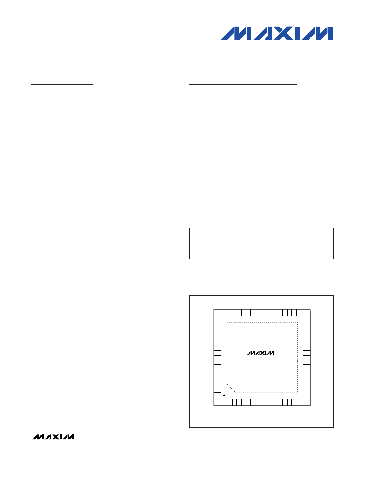
TOP VIEW
1
INB
2
COM33COM4
4
GND
5
INC
6
COM57COM6
8
SWITCH
24
NC323NO322NC421NO420NC519NO518NC617NO6
9
V+
10
IND
11
COM7
12
COM8
13
NO8
14
NC8
15
NO7
16
NC7
32
V+
31
INA
30
COM2
29
COM1
28
NC1
27
NO1
26
NC2
25
NO2
MAX4670
*EP
TQFN
*NOTE:
EXPOSED PADDLE
CONNECTED TO GND
Pin Configuration
Ordering Information
PART*
PINPACKAGE
SURGE
PKG
CODE
MAX4670ETJ
32 TQFN
YES T3255-4
*This part operates at a -40°C to +85°C temperature range.
Functional Diagram/Truth Table appears at end of data sheet.
PROTECTION
(5mm x 5mm)
MAX4670
Integrated T1/E1/J1 Short-Haul and
Long-Haul Protection Switch
2 _______________________________________________________________________________________
ABSOLUTE MAXIMUM RATINGS
Stresses beyond those listed under “Absolute Maximum Ratings” may cause permanent damage to the device. These are stress ratings only, and functional
operation of the device at these or any other conditions beyond those indicated in the operational sections of the specifications is not implied. Exposure to
absolute maximum rating conditions for extended periods may affect device reliability.
(All voltages referenced to GND.)
V+, IN_, SWITCH ......................................................-0.3V to +4V
COM_, NO_, NC_ (Note 1) ...........................-0.3V to (V+ + 0.3V)
Continuous Current
NO_, NC_, COM_ (Tx interface)..................................±150mA
NO_, NC_, COM_ (Rx interface) .................................±100mA
Peak Currents
NO_, NC_, COM_ (Tx interface)
(pulsed at 1ms, 10% duty cycle) ................................±300mA
NO_, NC_, COM_ (Rx interface)
(pulsed at 1ms, 10% duty cycle) ................................±200mA
Peak Surge Currents
Poised at 8µs ..................................................................21.4A
Poised at 20µs ................................................................11.9A
Continuous Power Dissipation (T
A
= +70°C)
32-Pin TQFN (derate 21.3mW/°C above +70°C) .......1702mW
38-Pin TSSOP (derate 13.7mW/°C above +70°C) .....1096mW
Operating Temperature Range ...........................-40°C to +85°C
Storage Temperature Range .............................-65°C to +150°C
Junction Temperature......................................................+150°C
Lead Temperature (soldering, 10s) .................................+300°C
ELECTRICAL CHARACTERISTICS
(V+ = +2.7V to +3.6V, TA= T
MIN
to T
MAX
, unless otherwise noted. Typical values are at TA= +25°C, unless otherwise noted.) (Notes 2, 3)
PARAMETER
CONDITIONS
UNITS
Rx INTERFACE
TA = +25°C59
On-Resistance R
ON
V
NO_
or V
NC_
= 1.5V
10
Ω
TA = +25°C 1.0
On-Resistance Match Between
Channels (Note 4)
∆R
ON
V
NO_
or V
NC_
= 1.5V
1.3
Ω
TA = +25°C 2.0 3.0
On-Resistance Flatness (Note 4)
)
V
NO_
or V
NC_
= 1.0V,
1.5V, 2.0V
3.4
Ω
)
NO_ or NC_ Off-Leakage
Current
)
V + = 3.6V ; V
C OM _
= 0.3V , 3.3V ;
V
N O_
or V
N C _
= 3.3V , 0.3V
-1 +1 µA
COM_ On-Leakage Current
)
V+ = 3.6V; V
COM_
= 0.3V, 3.3V;
V
NO_
or V
NC_
= 3.3V, 0.3V or floating
-1 +1 µA
Tx INTERFACE
TA = +25°C 0.7 0.9
On-Resistance (Note 5) R
ON
V
N O_
or V
N C _
= 1.5V
1.0
Ω
TA = +25°C
On-Resistance Match Between
Channels (Notes 3, 5)
∆R
ON
V
N O_
or V
N C _
= 1.5V
Ω
TA = +25°C 0.1
On-Resistance Flatness
(Notes 5, 6)
)
V+ = 3V;
I
COM_
= 100mA;
V
NO_
or V
NC_
= 1.0V,
1.5V, 2.0V
0.2
Ω
Note 1: Signals on NO_, NC_, COM_ exceeding V+ or GND are clamped by internal diodes. Limit forward-diode current to maximum
current rating.
SYM B O L
MIN TYP MAX
R
FLAT(ON
I
NO(OFF
I
NC (OFF
I
COM(ON
R
FLAT(ON
V+ = 3V, I
V+ = 3V, I
V+ = 3V; I
COM_
COM_
COM_
= 10mA,
= 10mA,
= 10mA;
V + = 3V , I
= 100m A,
C OM _
V + = 3V , I
= 100m A,
C OM _
TA = T
TA = T
TA = T
TA = T
TA = T
TA = T
to T
MIN
MAX
to T
MIN
MAX
to T
MIN
MAX
to T
MIN
MAX
0.03 0.150
to T
MIN
MAX
to T
MIN
MAX
0.175
0.18
MAX4670
Integrated T1/E1/J1 Short-Haul and
Long-Haul Protection Switch
_______________________________________________________________________________________ 3
ELECTRICAL CHARACTERISTICS (continued)
(V+ = +2.7V to +3.6V, TA= T
MIN
to T
MAX
, unless otherwise noted. Typical values are at TA= +25°C, unless otherwise noted.) (Notes 2, 3)
PARAMETER
SYM B O L
CONDITIONS
MIN
TYP
MAX
UNITS
NO_ or NC_ Off-Leakage
Current
),
)
V + = 3.6V ; V
C OM _
= 0.3V , 3.3V ;
V
N O_
or V
N C _
= 0.3V , 3.3V
-1 +1 µA
COM_ On-Leakage Current
)
V+ = 3.6V; V
COM_
= 0.3V, 3.3V;
V
NO_
or V
NC_
= 0.3V, 3.3V or floating
-1 +1 µA
DYNAMIC CHARACTERISTICS
TA = +25°C
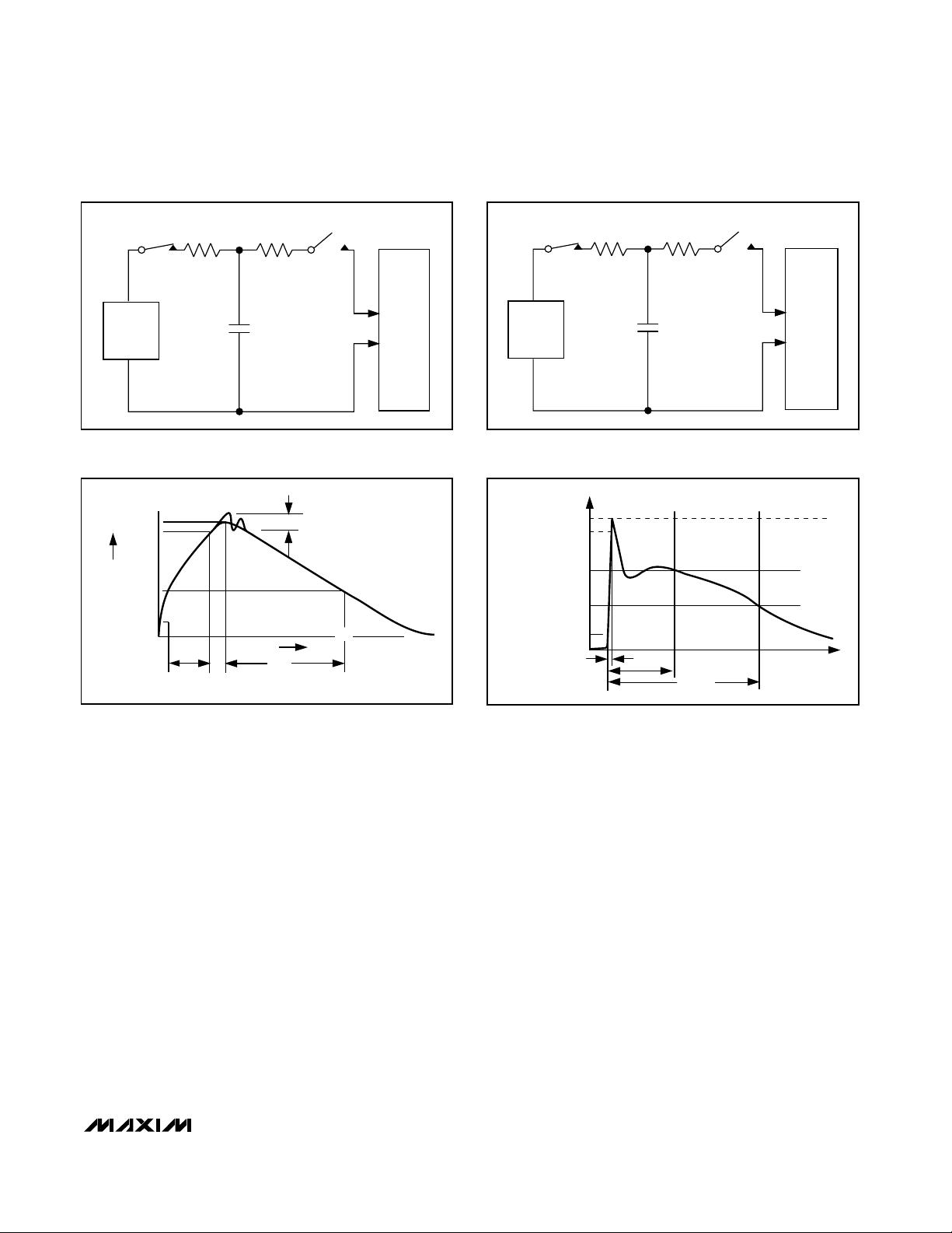
Turn-On Time t
ON
RL = 50Ω, C L = 35p F,
Fi g ur e 2
T
A
= T
MIN
to T
MAX
ns
TA = +25°C
Turn-Off Time t
OFF
RL = 50Ω,
TA = T
MIN
to T
MAX
ns
Break-Before-Make Delay t
D
RL = 50Ω, CL = 35pF, Figure 3 80 ns
Rx interface 8
Charge Injection Q
V
GE N
= 1.5V, R
GE N
=
Tx interface 20
pC
Rx interface
On-Channel
3dB Bandwidth
BW
Tx interface
MHz
V
ISO1
f < 3MHz
V
ISO2
Rx interface
R
L
= 50Ω, CL = 35pF,
3MHz < f < 30MHz
V
ISO1
f < 3MHz
Off-Isolation (Note 7)
V
ISO2
Tx interface
R
L
= 50Ω, CL = 35pF,
3MHz < f < 30MHz
dB
V
CT1
f < 3MHz
V
CT2
Rx interface,
Figure 5
3MHz < f < 30MHz
V
CT1
f < 3MHz
Crosstalk (Note 8)
V
CT2
Tx interface,
Figure 5
3MHz < f < 30MHz
dB
Rx interface f = 1MHz, Figure 6 12
NC_ or NO_ Off-Capacitance
Tx interface f = 1MHz, Figure 6 40
pF
Rx interface 24
COM_ On-Capacitance
f = 1MHz
Tx interface 60
pF
I
NO(OFF
I
NC(OFF
I
COM(ON
V
or V
N C _
= 1.5V ,
N O_
VNO or VNC = 1.5V,
CL = 35pF, Figure 2
0Ω, CL = 1nF, Fi gur e 4
300
RL = 50Ω, CL = 35pF,
RL = 50Ω, CL = 35pF,
RL = 50Ω, CL = 35pF,
RL = 50Ω, CL = 35pF,
300
-65
-58
-60
-40
-65
-50
C
OFFRX
C
OFFTX
C
C OM ( ON ) TX
C
C OM ( ON ) RX
RL = 50Ω, CL = 35pF,
RL = 50Ω, CL = 35pF,
-78
-30
400
750
200
750
MAX4670
Integrated T1/E1/J1 Short-Haul and
Long-Haul Protection Switch
4 _______________________________________________________________________________________
ELECTRICAL CHARACTERISTICS (continued)
(V+ = +2.7V to +3.6V, TA= T
MIN
to T
MAX
, unless otherwise noted. Typical values are at TA= +25°C, unless otherwise noted.) (Notes 2, 3)
PARAMETER
SYM B O L
CONDITIONS
MIN
TYP
MAX
UNITS
DIGITAL I/O (IN_, SWITCH )
Input-Low Voltage V
IL
V+ = 2.7V 0.5 V
Input-High Voltage V
IH
V+ = 3.6V 1.4 V
Input Leakage Current I
IL
V
IN_
= 0 or V+, V
S W I T C H
= 0 or V+ -1 +1 µA
SUPPLY
Operating Voltage Range V+ 2.7 3.6 V
Supply Current I+ V+ = 3.6V, V
IN_
= V
S W I T C H
= 0 or V+ 10 µA
Note 2: The algebraic convention is used in this data sheet. The most negative value is shown in the minimum column.
Note 3: Devices are 100% tested at hot and room and guaranteed by design at cold.
Note 4: ∆R
ON
= R
ON(MAX)
- R
ON(MIN)
.
Note 5: Guaranteed by design.
Note 6: Flatness is defined as the difference between the maximum and minimum value of on-resistance as measured over the
specified analog signal ranges.
Note 7: Off-isolation = 20log
10[VCOM_
/ (V
NO_
or V
NC_
)], V
COM_
= output, V
NO_
or V
NC_
= input to off switch.
Note 8: Crosstalk between any two switches.
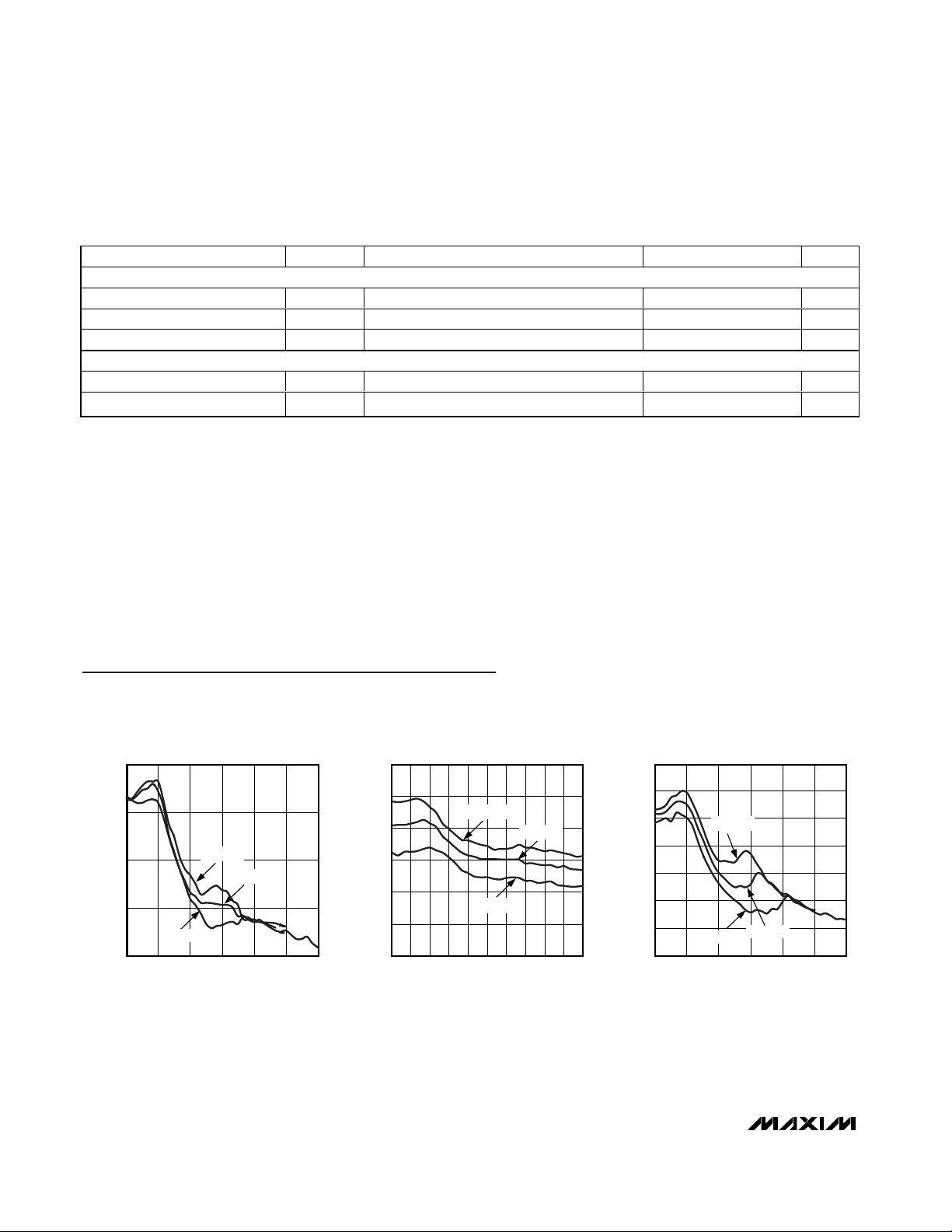
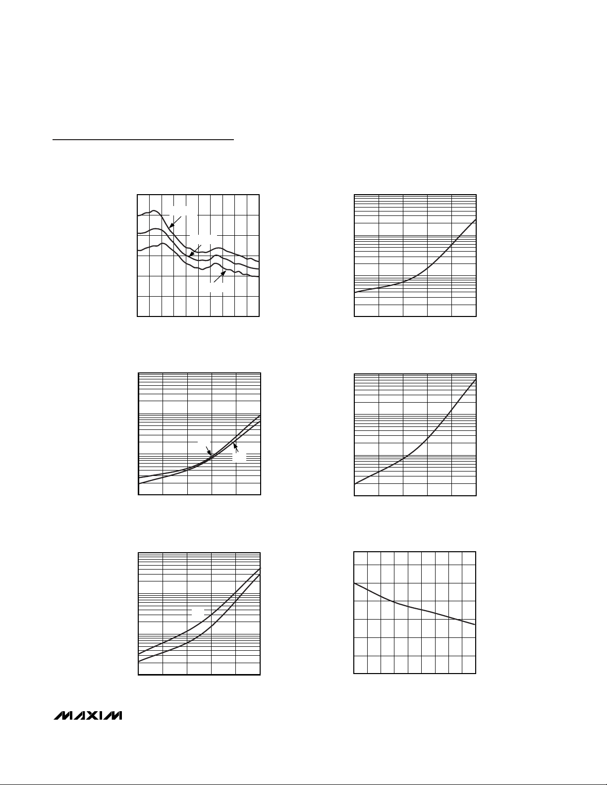
Typical Operating Characteristics
(V+ = 3.0V, TA= +25°C, unless otherwise noted.)
ON-RESISTANCE
vs. COM_VOLTAGE (Tx INTERFACE)
MAX4670 toc01
V
COM_
(V)
ON-RESISTANCE (Ω)
3.01.2 1.8 2.40.6
0.6
0.7
0.8
0.9
0.5
03.6
V+ = 3V
V+ = 2.7V
V+ = 3.6V
ON-RESISTANCE vs. COM_ VOLTAGE
OVER TEMPERATURE (Tx INTERFACE)
MAX4670 toc02
V
COM_
(V)
ON-RESISTANCE (Ω)
2.72.42.11.81.51.20.90.60.3
0.2
0.4
0.6
0.8
1.0
1.2
0
0 3.0
TA = +85°C
TA = +25°C
TA = -40°C
ON-RESISTANCE
vs. COM_VOLTAGE (Rx INTERFACE)
MAX4670 toc03
V
COM_
(V)
ON-RESISTANCE (Ω)
3.01.2 1.8 2.40.6
4
5
6
7
8
9
10
3
0 3.6
V+ = 3.6V
V+ = 2.7V
V+ = 3V
MAX4670
Integrated T1/E1/J1 Short-Haul and
Long-Haul Protection Switch
_______________________________________________________________________________________ 5
ON-RESISTANCE vs. COM_ VOLTAGE
OVER TEMPERATURE (Rx INTERFACE)
MAX4670 toc04
V
COM_
(V)
ON-RESISTANCE (Ω)
2.72.42.11.81.51.20.90.60.3
2
4
6
8
10
12
0
0 3.0
TA = +85°C
TA = +25°C
TA = -40°C
10
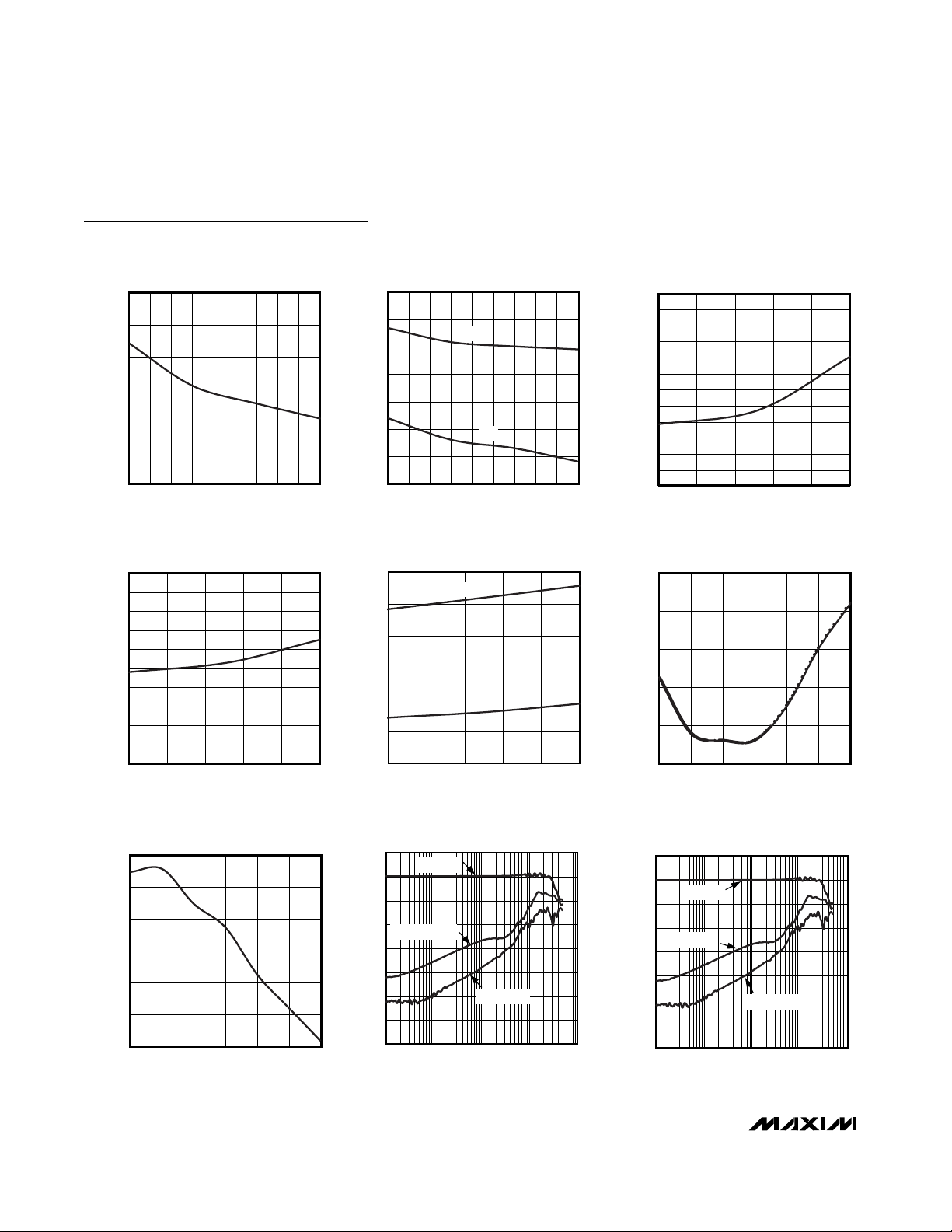
0.01
-40 35 85
COM_ LEAKAGE CURRENT
vs. TEMPERATURE (Tx INTERFACE)
0.1
1
MAX4670toc05
TEMPERATURE (°C)
LEAKAGE CURRENT (nA)
-15 6010
10
0.01
-40 35 85
NC_/NO_ LEAKAGE CURRENT
vs. TEMPERATURE (Tx INTERFACE)
0.1
1
MAX4670toc06
TEMPERATURE (°C)
LEAKAGE CURRENT (nA)
-15 6010
NC_
NO_
COM_ LEAKAGE CURRENT
vs. TEMPERATURE (Rx INTERFACE)
MAX4670 toc07
TEMPERATURE (°C)
LEAKAGE CURRENT (nA)
603510-15
0.1
1
10
0.01
-40 85
NC_/NO_ LEAKAGE CURRENT
vs. TEMPERATURE (Rx INTERFACE)
MAX4670 toc08
TEMPERATURE (°C)
LEAKAGE CURRENT (nA)
603510-15
0.1
1
10
0.01
-40 85
NC_
NO_
TURN-ON TIME
vs. SUPPLY VOLTAGE (Tx INTERFACE)
MAX4670 toc09
SUPPLY VOLTAGE (V)
TURN-ON TIME (ns)
3.53.43.33.23.13.02.92.8
130
160
190
220
250
280
100
2.7 3.6
Typical Operating Characteristics (continued)
(V+ = 3.0V, TA= +25°C, unless otherwise noted.)
MAX4670
Integrated T1/E1/J1 Short-Haul and
Long-Haul Protection Switch
6 _______________________________________________________________________________________
TURN-ON/OFF TIMES
vs. TEMPERATURE (Rx INTERFACE)
MAX4670 toc14
TEMPERATURE (°C)
TURN-ON/OFF TIMES (ns)
603510-15
10
20
30
40
50
60
0
-40 85
t
ON
t
OFF
CHARGE INJECTION
vs. COM_ VOLTAGE (Tx INTERFACE)
MAX4670 toc15
V
COM
(V)
CHARGE INJECTION (pC)
2.52.01.51.00.5
30
60
90
120
150
0
0 3.0
CHARGE INJECTION
vs. COM_ VOLTAGE (Rx INTERFACE)
MAX4670 toc16
V
COM_
(V)
CHARGE INJECTION (pC)
2.52.01.51.00.5
2
4
6
8
10
12
0
0 3.0
FREQUENCY RESPONSE
(Tx INTERFACE)
FREQUENCY (MHz)
ON LOSS (dB)
MAX4670 toc17
-140
-120
-100
-80
-60
-40
-20
0
20
0.1 1 10 100 1000
ON LOSS
OFF-ISOLATIONOFF-ISOLATION
CROSSTALK
FREQUENCY RESPONSE
(Rx INTERFACE)
FREQUENCY (MHz)
ON LOSS (dB)
MAX4670 toc18
-140
-120
-100
-80
-60
-40
-20
0
20
0.1 1 10 100 1000
ON LOSS
OFF-ISOLATIONOFF-ISOLATION
CROSSTALK
Typical Operating Characteristics (continued)
(V+ = 3.0V, TA= +25°C, unless otherwise noted.)
TURN-OFF TIME
vs. SUPPLY VOLTAGE (Tx INTERFACE)
MAX4670 toc10
SUPPLY VOLTAGE (V)
TURN-OFF TIME (ns)
3.53.43.33.23.13.02.92.8
10
20
30
40
50
60
0
2.7 3.6
TURN-ON TIME
vs. TEMPERATURE (Tx INTERFACE)
MAX4670 toc12
TEMPERATURE (°C)
TURN-ON TIME (ns)
603510-15
150
175
200
250
300
350
225
275
325
375
125
400
100
-40 85
V+ = 3V
TURN-ON/OFF TIMES
vs. SUPPLY VOLTAGE (Rx INTERFACE)
MAX4670 toc11
SUPPLY VOLTAGE (V)
TURN-ON/OFF TIMES (ns)
3.43.33.23.13.02.92.8
65
70
75
80
85
90
95
60
2.7 3.5
3.6
t
ON
t
OFF
TURN-OFF TIME
vs. TEMPERATURE (Tx INTERFACE)
MAX4670 toc13
TEMPERATURE (°C)
TURN-OFF TIME (ns)
603510-15
22
24
28
32
36
26
30
34
38
40
20
-40 85
V+ = 3V

MAX4670
Integrated T1/E1/J1 Short-Haul and
Long-Haul Protection Switch
_______________________________________________________________________________________ 7
PIN NAME FUNCTION
— N.C. No Connection. Not internally connected.
1 INB
Transmitter 1 Logic Control. Drive INB high to connect NC3 and NC4. INB logic is ignored
when SWITCH asserts low.
2 COM3
Common Terminal 3. Transmitter 1 positive differential terminal. Connect COM3 to the transmit
interface transformer.
3 COM4
Common Terminal 4. Transmitter 1 negative differential terminal. Connect COM4 to the
transmit interface transformer.
4 GND Ground
5INC
Transmitter 2 Logic Control. Drive INC high to connect NC5 and NC6. INC logic is ignored
when SWITCH asserts low.
6 COM5
Common Terminal 5. Transmitter 2 positive differential terminal. Connect COM5 to the transmit
interface transformer.
7 COM6
Common Terminal 6. Transmitter 2 negative differential terminal. Connect COM6 to the
transmit interface transformer.
8 SWITCH
Protection Switch Control. Assert SWITCH low to connect all switches to protection bus. When
SWITCH asserts low, SWITCH overrides all IN_ inputs. Assert SWITCH high to enable all
switches and let the respective IN control the switches.
9, 32 V+ Positive Supply Voltage. Bypass V+ to ground with a 0.1µF ceramic capacitor.
10 IND
Receiver 2 Logic Control. Drive IND high to connect NC7 and NC8. IND logic is ignored when
SWITCH asserts low.
11 COM7
Common Terminal 7. Receiver 2 positive differential terminal. Connect COM7 to the receive
interface transformer.
12 COM8
Common Terminal 8. Receiver 2 negative differential terminal. Connect COM8 to the receive
interface transformer.
13 NO8
Normally Open Terminal 8. Receiver 2 differential protection terminal. Connect NO8 to the
protection bus.
14 NC8 Normally Closed Terminal 8. Receiver 2 differential terminal. Connect NC8 to LIU receiver.
15 NO7
Normally Open Terminal 7. Receiver 2 differential protection terminal. Connect NO7 to the
protection bus.
16 NC7 Normally Closed Terminal 7. Receiver 2 differential terminal. Connect NC7 to LIU receiver.
17 NO6
Normally Open Terminal 6. Transmitter 2 differential protection terminal. Connect NO6 to the
protection bus.
18 NC6 Normally Closed Terminal 6. Transmitter 2 differential terminal. Connect NC6 to LIU receiver.
19 NO5
Normally Open Terminal 5. Transmitter 2 differential protection terminal. Connect NO5 to the
protection bus.
20 NC5 Normally Closed Terminal 5. Transmitter 2 differential terminal. Connect NC5 to LIU receiver.
21 NO4
Normally Open Terminal 4. Transmitter 1 differential protection terminal. Connect NO4 to the
protection bus.
Pin Description

MAX4670
Detailed Description
The MAX4670 is a quad-DPDT/octal-SPDT analog switch
optimized for T1/E1/J1 line-card redundancy protection
applications. This analog switch is configurable as two
differential transmitter and receiver pairs utilized in
T1/E1/J1 redundancy architecture.
The MAX4670 has four low 0.7Ω on-resistance switches
with 60pF and 40pF on- and off-capacitances, respectively, for interfacing to the LIU transmitter inputs. The
MAX4670 also includes four 5Ω on-resistance switches
with low 24pF and 12pF on- and off-capacitances,
respectively, for interfacing to the LIU receiver inputs.
The MAX4670 replaces two diode arrays or two transient voltage suppressors and four dual-SPDT relays,
significantly reducing board space and simplifying PC
board routing. The MAX4670 pinouts are targeted for
T1/E1/J1 applications, resulting in a simplified layout
when interfacing with standard line transformers and
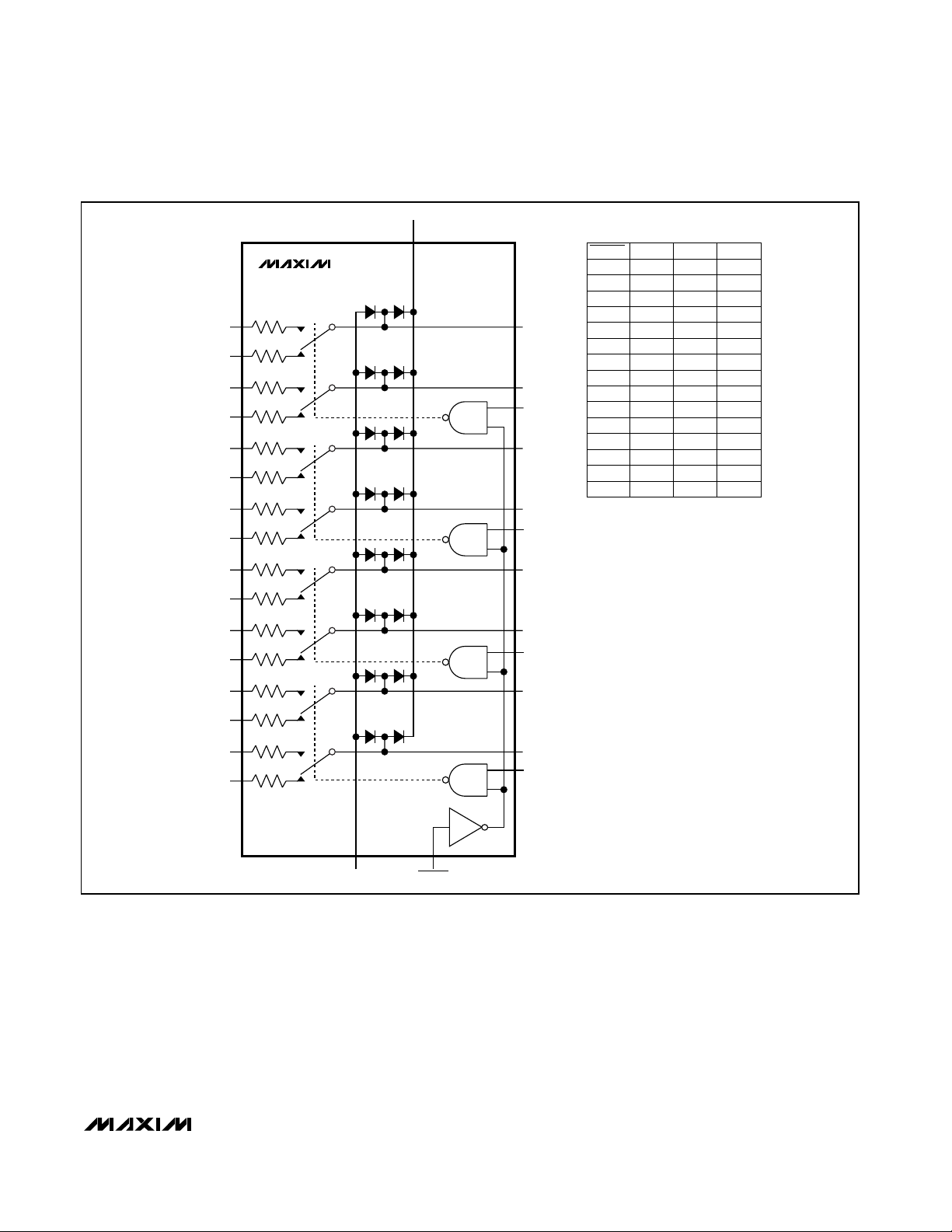
LIUs. Figure 1 is the functional diagram.
Logic Inputs (IN_,
SWITCH
)
The MAX4670 four logic inputs (IN_) control the switches
in pairs and contain a global logic input (SWITCH) that
connects all COMs to their respective NO_ inputs.
SWITCH overrides all IN_ inputs when asserted low, thus
connecting all NO_ to COM_ outputs (transmitter/receiver
pairs to the protection bus). When SWITCH asserts high,
IN_ controls the switch pairs. See Table 1.
Surge Protection
The MAX4670 includes chip-side, surge-protection capability for short-haul intrabuilding applications. The lowcapacitance diodes suppress surge residuals from the
primary, line-side protection devices. It is assumed that
adequate primary protection is included on the line die of
the transformer, as represented in Figures 7–10. Table 2
lists the applicable surge protection setups for E1
interfaces. The MAX4670 surge test was performed per
IEC 61000-4-5 Class 2 specifications and passed at ±1kV
with only an in-line transformer and primary surge suppressor. The transformer was a Halo TG83-1505NX transformer and the surge suppressor was a Teccor P0640SC.
Applications Information
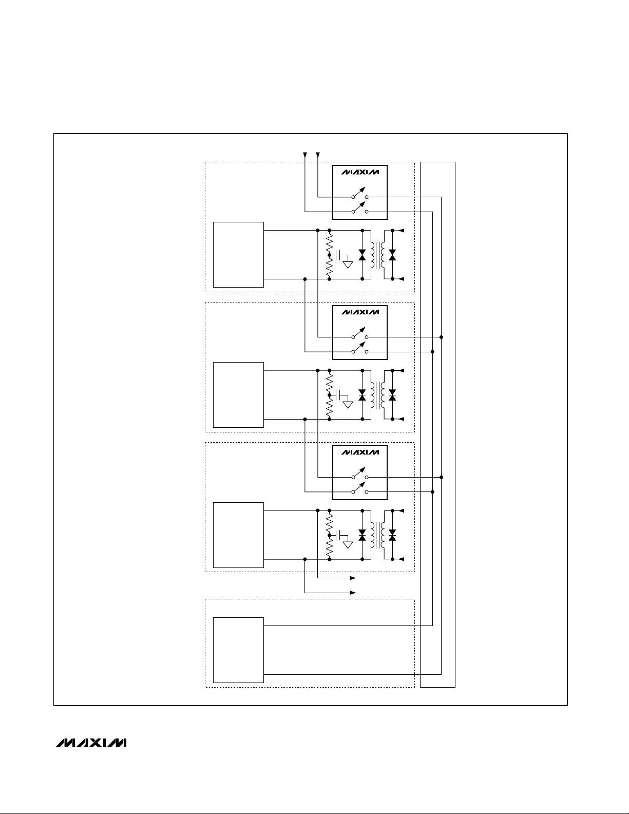
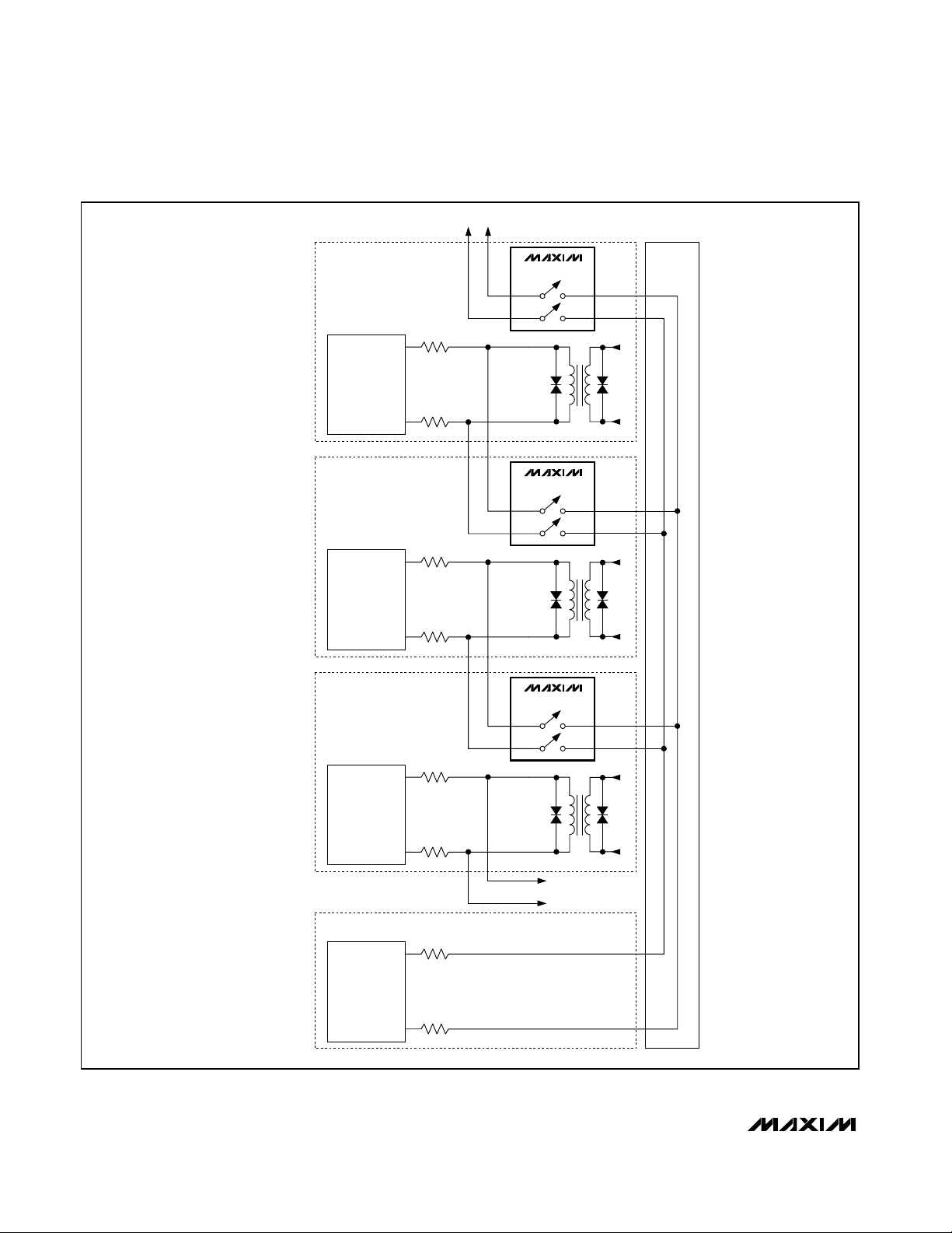
Redundancy Architecture
Figures 7 through 10 illustrate the MAX4670 used in two
different redundancy architectures. There is one backup card for up to N line cards in the system (in this
example, N = 3). In the event one of the line cards fails
(memory failure, power supply went down, etc.), a system supervisory card issues a command to the switches to reroute the traffic to and from the problem line
card to the backup line card.
Integrated T1/E1/J1 Short-Haul and
Long-Haul Protection Switch
8 _______________________________________________________________________________________
PIN NAME FUNCTION
22 NC4 Normally Closed Terminal 4. Transmitter 1 differential terminal. Connect NC4 to LIU receiver.
23 NO3
Normally Open Terminal 3. Transmitter 1 differential protection terminal. Connect NO3 to the
protection bus.
24 NC3 Normally Closed Terminal 3. Transmitter 1 differential terminal. Connect NC3 to LIU receiver.
25 NO2
N or m al l y Op en Ter m i nal 2. Recei ver 2 differential protection terminal. C onnect NO2 to the
p r otecti on b us.
26 NC2 Normally Closed Terminal 2. Receiver 1 differential terminal. Connect NC2 to LIU receiver.
27 NO1
N or m al l y Op en Ter m i nal 1. Recei ver 1 differential protection terminal. C onnect NO1 to the
p r otecti on b us.
28 NC1 Normally Closed Terminal 1. Receiver 1 differential terminal. Connect NC1 to LIU receiver.
29 COM1
Common Terminal 1. Receiver 1 positive differential terminal. Connect COM1 to the receive
interface transformer.
30 COM2
Common Terminal 2. Receiver 1 negative differential terminal. Connect COM2 to the receive
interface transformer.
31 INA
Receiver 1 Logic Control. Drive INA low to connect receiver 1 to the LIU. INA logic is ignored
when SWITCH asserts low.
EP EP Exposed Paddle. Connect EP to GND or leave unconnected.
Pin Description (continued)
In a switching-card architecture, a common switching
card contains all the protection switches for the T1/E1/J1
lines entering the system (see Figures 7 and 8).
With an adjacent card architecture, the switches protecting any given line card reside physically in the adjacent line card (see Figures 9 and 10).
Receive and transmit interfaces reside in the same
board for each T1/E1/J1 port. The diagrams represent
the typical interface transformers and resistors recommended for Dallas/Maxim LIUs, such as the DS21Q55.
The protection switches are placed in the low-voltage
side of the transformer to meet the isolation requirements. Note that there is also a TVS in the line side of
the transformers. The receive and transmit resistors provide impedance matching to the T1/E1/J1 transmission
cable characteristic impedance. Refer to Application
Note 2857 for more information on T1/E1/J1 applications.
MAX4670
Integrated T1/E1/J1 Short-Haul and
Long-Haul Protection Switch
_______________________________________________________________________________________ 9
MAX4670
NO1
R
X
NC1
COM1
NO2
R
X
NC2
COM2
INA
INB
INC
IND
NO3
T
X
NC3
COM3
NO4
T
X
NC4
COM4
NO5
T
X
NC5
COM5
NO6
T
X
NC6
COM6
NO7
R
X
NC7
COM7
NO8
R
X
NC8
COM8
0.6
Ω
0.6
Ω
0.6
Ω
0.6
Ω
0.6
Ω
0.6
Ω
0.6
Ω
0.6
Ω
V+
GND SWITCH
INA NC1/NC2 NO1/NO2
LOW X OFF ON
HIGH LOW OFF ON
HIGH HIGH ON OFF
INB NC3/NC4 NO3/NO4
LOW X OFF ON
HIGH LOW OFF ON
HIGH HIGH ON OFF
INC NC5/NC6 NO5/NO6
LOW X OFF ON
HIGH LOW OFF ON
HIGH HIGH ON OFF
IND NC7/NC8 NO7/NO8
LOW X OFF ON
HIGH LOW OFF ON
HIGH HIGH ON OFF
SWITCH
Figure 1. Functional Diagram

MAX4670
LIU Interface Recommendations
The MAX4670 low 0.7Ω (typ) on-resistance is adequate, even in applications where the LIUs require no
external series transmit resistors (Rt = 0 in Figures 8
and 10). However, in some instances, increase the LIU
output amplitude to compensate for R
ON
if the LIU supports programmable output amplitude. With LIUs
requiring external transmit resistors, it is recommended
to reduce Rt by the amount of the typical R
ON
with LIUs
requiring external transmit resistors.
For example, if the LIU vendor recommends Rt = 9.1Ω,
the actual value in the application should be:
Rt = Rt – R
ON
= 9.1Ω - 0.7 = 8.4Ω
The receive interface series resistance is small enough
to support LIUs with internal line termination, provided
the external 120Ω parallel resistor combination (Rr) is
connected, as shown in Figures 7 and 9.
While in normal operation, the MAX4670 requires the
input and output signals to be within the V+ and GND
supply rails.
ESD Test Conditions
ESD performance depends on a variety of conditions.
Contact Maxim for a reliability report that documents
test setup, test methodology, and test results.
Human Body Model
Figure 11 shows the Human Body Model. Figure 12
shows the current waveform it generates when discharged into a low impedance. This model consists of a
100pF capacitor charged to the ESD voltage of interest,
which is then discharged into the test device through a
1.5kΩ resistor.
IEC 1000-4-2
The IEC 1000-4-2 standard covers ESD testing and
performance of finished equipment. It does not specifically refer to ICs. The major difference between tests
done using the Human Body Model and IEC 1000-4-2
is a higher peak current in IEC 1000-4-2, because
series resistance is lower in the IEC 1000-4-2 model.
Hence, the ESD withstands voltage measured to IEC
61000-4-2, and is generally lower than that measured
using the Human Body Model. Figure 13 shows the IEC
61000-4-2 model, and Figure 14 shows the current
waveform for the ±8kV IEC, 61000-4-2 Level 4, ESD
Contact Discharge test. The Air-Gap test involves
approaching the device with a charged probe. The
Contact Discharge method connects the probe to the
device before the probe is energized.
Machine Model
The Machine Model for ESD tests all pins using a
200pF storage capacitor and zero discharge resistance. Its objective is to emulate the stress caused by
contact that occurs with handling and assembly during
manufacturing.
Integrated T1/E1/J1 Short-Haul and
Long-Haul Protection Switch
10 ______________________________________________________________________________________
Table 1. MAX4670 Truth Table
SWITCH INA NC1/NC2 NO1/NO2
LOW X OFF ON
HIGH LOW OFF ON
HIGH HIGH ON OFF
— INB NC3/NC4 NO3/NO4
LOW X OFF ON
HIGH LOW OFF ON
HIGH HIGH ON OFF
— INC NC5/NC6 NO5/NC6
LOW X OFF ON
HIGH LOW OFF ON
HIGH HIGH ON OFF
— IND NC7/NC8 NO7/NO8
LOW X OFF ON
HIGH LOW OFF ON
HIGH HIGH ON OFF
Table 2. IEC 61000-4-5 Test Conditions
TEST CONFIGURATION TEST CONDITIONS
Differential Surge
(Line to Line)
500V peak, 12A min current,
8µs/20µs surge
Common-Mode Surge
(Line to GND)
1000V peak, 24A min current,
8µs/20µs surge
MAX4670
Integrated T1/E1/J1 Short-Haul and
Long-Haul Protection Switch
______________________________________________________________________________________ 11
tr < 5ns
tf < 5ns
50%
V
INL
LOGIC
INPUT
R
L
50
Ω
COM_
GND
IN_
C
L
INCLUDES FIXTURE AND STRAY CAPACITANCE.
V
OUT
= V
N_ (
R
L
)
RL + R
ON
WHERE, VN_ IS V
NC_
OR V
NO_
.
V
INH
t
OFF
0V
NO_
OR NC_
V
NO_
OR
V
NC_
0.9 × V
0UT
0.9 × V
OUT
t
ON
V
OUT
SWITCH
OUTPUT
LOGIC
INPUT
LOGIC INPUT WAVEFORMS INVERTED FOR SWITCHES
THAT HAVE THE OPPOSITE LOGIC SENSE.
V+
C
L
35pF
V
OUT
MAX4670
0.1µF
V+
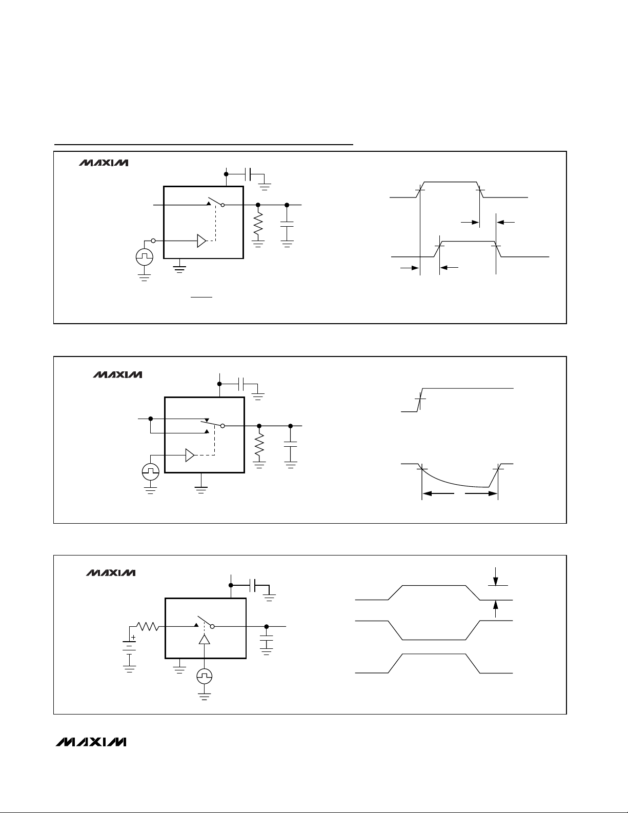
Figure 2. Switching Time
50%
V
INH
V
INL
LOGIC
INPUT
V
OUT
0.9 × V
OUT
t
D
LOGIC
INPUT
R
L
50
Ω
GND
C
L
INCLUDES FIXTURE AND STRAY CAPACITANCE.
NO_
IN_
NC_
V
OUT
V+
C
L
35pF
V
NO_
OR
V
NC_
COM_
MAX4670
0.1µF
V+
Figure 3. Break-Before-Make Intervals
Test Circuits/Timing Diagrams
V
OUT
IN_
OFF
ON
OFF
∆
V
OUT
Q = (∆V
OUT
)(CL)
IN DEPENDS ON SWITCH CONFIGURATION;
INPUT POLARITY DETERMINED BY SENSE OF SWITCH.
OFF
ON
OFF
IN_
MAX4670
V
GEN
GND
COM_
C
L
V
OUT
V+
NC_
OR NO_
V
INL
TO V
INH
R
GEN
IN_
0.1µF
V+
Figure 4. Charge Injection

MAX4670
Integrated T1/E1/J1 Short-Haul and
Long-Haul Protection Switch
12 ______________________________________________________________________________________
CAPACITANCE
METER
NC_ OR
NO_
COM_
GND
IN_
V
INL
OR
V
INH
0.1µF
V+
f = 1MHz
V+
MAX4670
Figure 6. Channel Off-/On-Capacitance
Test Circuits/Timing Diagrams (continued)
MEASUREMENTS ARE STANDARDIZED AGAINST SHORTS AT IC TERMINALS.
OFF-ISOLATION IS MEASURED BETWEEN COM_ AND "OFF" NO_ OR NC_ TERMINAL ON EACH SWITCH.
ON-LOSS IS MEASURED BETWEEN COM_ AND "ON" NO_ OR NC_TERMINAL ON EACH SWITCH.
CROSSTALK IS MEASURED FROM ONE CHANNEL TO ALL OTHER CHANNELS.
SIGNAL DIRECTION THROUGH SWITCH IS REVERSED; WORST VALUES ARE RECORDED.
+3V
V
OUT
V+
IN_
NC_
NO_
COM_
V
IN
MAX4670
OFF-ISOLATION = 20log
V
OUT
V
IN
ON-LOSS = 20log
V
OUT
V
IN
CROSSTALK = 20log
V
OUT
V
IN
NETWORK
ANALYZER
50
Ω
50
Ω
50
Ω
50
Ω
MEAS REF
0.1µF
0 OR V+
50
Ω
GND
Figure 5. On-Loss, Off-Isolation, and Crosstalk

MAX4670
Integrated T1/E1/J1 Short-Haul and
Long-Haul Protection Switch
______________________________________________________________________________________ 13
COM1
COM2
U1
1:1
U1
1:1
U2
1:1
NC1
NO1
NC2
NO2
LINE CARD 1
RTIP
RRING
LIU R
X
COM7
COM8
NC7
NO7
NC8
NO8
LINE CARD 2
RTIP
RRING
LIU R
X
COM7
COM8
NC7
NO7
NC8
NO8
LINE CARD 3
RTIP
RRING
LIU R
X
BACKUP LINE CARD
RTIP
RRING
LIU R
X
PROTECTION SWITCHING CARD PROTECTION BUS
Rr
Rr
Rr
Rr
Rr
Rr
Figure 7. Switching-Card-Architecture Receive Path
RECEIVE PATH

MAX4670
Integrated T1/E1/J1 Short-Haul and
Long-Haul Protection Switch
14 ______________________________________________________________________________________
COM3
COM4
NO3
NC3
NO4
NC4
LINE CARD 1
TRING
TTIP
LIU T
X
PROTECTION SWITCHING CARD PROTECTION BUS
R
T
R
T
COM5
COM6
NO5
NC5
NO6
NC6
LINE CARD 2
TRING
TTIP
LIU T
X
R
T
R
T
COM5
COM6
NO5
NC5
NO6
NC6
LINE CARD 3
TRING
TTIP
LIU T
X
R
T
R
T
BACKUP LINE CARD
TTIP
TRING
LIU T
X
U1
1:1
U1
1:1
U2
1:1
Figure 8. Switching-Card-Architecture Transmit Path
TRANSMIT PATH
MAX4670
Integrated T1/E1/J1 Short-Haul and
Long-Haul Protection Switch
______________________________________________________________________________________ 15
1:1
COM1
Rr
Rr
Rr
Rr
Rr
Rr
NO1
COM2 NO2
MAX4670
RTIP
RRING
LIU R
X
LINE CARD 1
1:1
COM1 NO1
COM2 NO2
MAX4670
RTIP
RRING
LIU R
X
LINE CARD 2
1:1
COM1 NO1
COM2 NO2
MAX4670
RTIP
RRING
LIU R
X
LINE CARD 3
RTIP
RRING
LIU R
X
BACKUP LINE CARD
PROTECTION
BUS
Figure 9. Adjacent-Card-Architecture Receive Path
RECEIVE PATH
MAX4670
Integrated T1/E1/J1 Short-Haul and
Long-Haul Protection Switch
16 ______________________________________________________________________________________
1:2
R
T
R
T
COM3 NO3
COM4 NO4
MAX4670
TTIP
TRING
LIU Tx
LINE CARD 1
1:2
R
T
R
T
COM3 NO3
COM4 NO4
MAX4670
TTIP
TRING
LIU Tx
LINE CARD 2
1:2
R
T
R
T
COM3 NO3
COM4 NO4
MAX4670
TTIP
TRING
LIU Tx
LINE CARD 3
R
T
R
T
RTIP
RRING
LIU Tx
BACKUP LINE CARD
PROTECTION
BUS
Figure 10. Adjacent-Card-Architecture Transmit Path
TRANSMIT PATH
MAX4670
Integrated T1/E1/J1 Short-Haul and
Long-Haul Protection Switch
______________________________________________________________________________________ 17
CHARGE-CURRENT-
LIMIT RESISTOR
DISCHARGE
RESISTANCE
STORAGE
CAPACITOR
C
s
100pF
R
C
1MΩ
R
D
1500Ω
HIGH-
VOLTAGE
DC
SOURCE
DEVICE
UNDER
TEST
Figure 11. Human Body ESD Test Model
IP 100%
90%
36.8%
t
RL
TIME
t
DL
CURRENT WAVEFORM
PEAK-TO-PEAK RINGING
(NOT DRAWN TO SCALE)
I
r
10%
0
0
AMPERES
Figure 12. Human Body Model Current Waveform
CHARGE-CURRENT-
LIMIT RESISTOR
DISCHARGE
RESISTANCE
STORAGE
CAPACITOR
C
s
150pF
R
C
50MΩ TO 100MΩ
R
D
330Ω
HIGH-
VOLTAGE
DC
SOURCE
DEVICE
UNDER
TEST
Figure 13. IEC 1000-4-2 ESD Test Model
tr = 0.7ns TO 1ns
30ns
60ns
t
100%
90%
10%
I
PEAK
I
Figure 14. IED 1000-4-2 ESD Generator Current Waveform
MAX4670
Integrated T1/E1/J1 Short-Haul and
Long-Haul Protection Switch
18 ______________________________________________________________________________________
Chip Information
PROCESS: CMOS
MAX4670
NO1
R
X
NC1
COM1
NO2
R
X
NC2
COM2
INA
INB
INC
IND
NO3
T
X
NC3
COM3
NO4
T
X
NC4
COM4
NO5
T
X
NC5
COM5
NO6
T
X
NC6
COM6
NO7
R
X
NC7
COM7
NO8
R
X
NC8
COM8
0.6
Ω
0.6
Ω
0.6
Ω
0.6
Ω
0.6
Ω
0.6
Ω
0.6
Ω
0.6
Ω
V+
GND SWITCH
INA NC1/NC2 NO1/NO2
LOW X OFF ON
HIGH LOW OFF ON
HIGH HIGH ON OFF
INB NC3/NC4 NO3/NO4
LOW X OFF ON
HIGH LOW OFF ON
HIGH HIGH ON OFF
INC NC5/NC6 NO5/NO6
LOW X OFF ON
HIGH LOW OFF ON
HIGH HIGH ON OFF
IND NC7/NC8 NO7/NO8
LOW X OFF ON
HIGH LOW OFF ON
HIGH HIGH ON OFF
SWITCH
Functional Diagram/Truth Table

MAX4670
Integrated T1/E1/J1 Short-Haul and
Long-Haul Protection Switch
______________________________________________________________________________________ 19
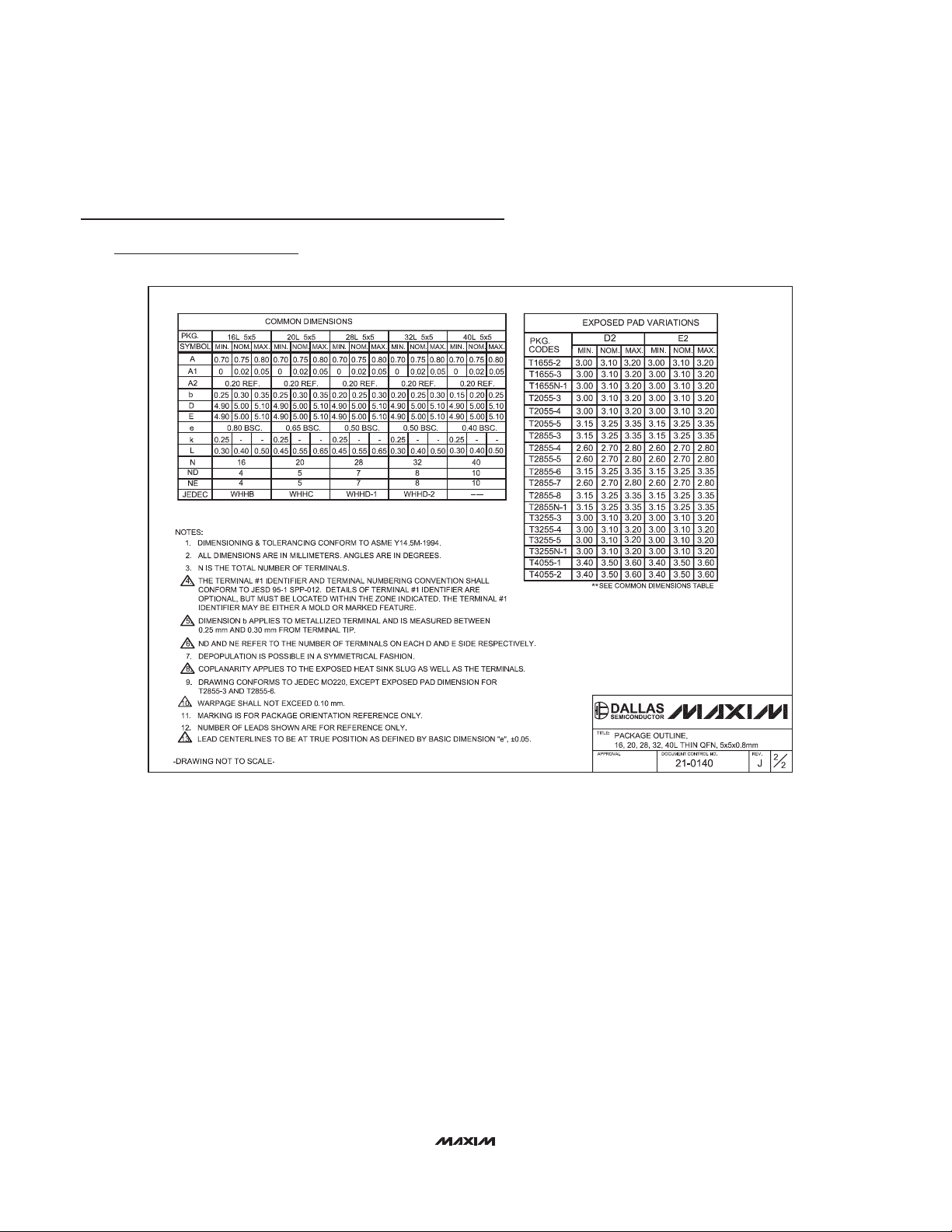
Package Information (continued)
(The package drawing(s) in this data sheet may not reflect the most current specifications. For the latest package outline information,
go to www.maxim-ic.com/packages
.)
QFN THIN.EPS
MAX4670
Integrated T1/E1/J1 Short-Haul and
Long-Haul Protection Switch
Maxim cannot assume responsibility for use of any circuitry other than circuitry entirely embodied in a Maxim product. No circuit patent licenses are
implied. Maxim reserves the right to change the circuitry and specifications without notice at any time.
20 ____________________Maxim Integrated Products, 120 San Gabriel Drive, Sunnyvale, CA 94086 408-737-7600
© 2006 Maxim Integrated Products is a registered trademark of Maxim Integrated Products, Inc.
Maxim cannot assume responsibility for use of any circuitry other than circuitry entirely embodied in a Maxim product. No circuit patent licenses are
implied. Maxim reserves the right to change the circuitry and specifications without notice at any time.
20 ____________________Maxim Integrated Products, 120 San Gabriel Drive, Sunnyvale, CA 94086 408-737-7600
© 2005 Maxim Integrated Products is a registered trademark of Maxim Integrated Products, Inc.
Package Information (continued)
(The package drawing(s) in this data sheet may not reflect the most current specifications. For the latest package outline information,
go to www.maxim-ic.com/packages
.)
 Loading...