19-0219; Rev 2; 6/94
EVALUATION KIT MANUAL
FOLLOWS DATA SHEET
RGB Video Switches and Buffers
_______________General Description
The MAX463–MAX470 series of two-channel,
triple/quad buffered video switches and video buffers
combines high-accuracy, unity-gain-stable amplifiers
with high-performance video switches. Fast switching
time and low differential gain and phase error make this
series of switches and buffers ideal for all video applications. The devices are all specified for ±5V supply
operation with inputs and outputs as high as ±2.5V
when driving 150Ω loads (75Ω back-terminated cable).
Input capacitance is typically only 5pF, and channel-tochannel crosstalk is better than 60dB, accomplished by
surrounding all inputs with AC ground pins. The onboard amplifiers feature a 200V/µs slew rate (300V/µs
for AV= 2V/V amplifiers), and a bandwidth of 100MHz
(90MHz for AV= 2V/V buffers). Channel selection is
controlled by a single TTL-compatible input pin or by a
microprocessor interface, and channel switch time is
only 20ns.
For design flexibility, devices are offered with bufferamplifier gains of 1V/V or 2V/V for 75Ω back-terminated
applications. Output amplifiers have a guaranteed output swing of ±2V into 75Ω.
Devices offered in this series are as follows:
PART DESCRIPTION
MAX463 Triple RGB Switch & Buffer 1
MAX464 Quad RGB Switch & Buffer 1
MAX465 Triple RGB Switch & Buffer 2
MAX466 Quad RGB Switch & Buffer 2
MAX467 Triple Video Buffer 1
MAX468 Quad Video Buffer 1
MAX469 Triple Video Buffer 2
MAX470 Quad Video Buffer 2
VOLTAGE GAIN
(V/V)
________________________Applications
Broadcast-Quality Color-Signal Multiplexing
RGB Multiplexing
RGB Color Video Overlay Editors
RGB Color Video Security Systems
RGB Medical Imaging
Coaxial-Cable Line Drivers
Two-Channel, Triple/Quad
____________________________Features
♦ 100MHz Unity-Gain Bandwidth
♦ 90MHz Bandwidth with 2V/V Gain
♦ 0.01%/0.03° Differential Gain/Phase Error
♦ Drives 50Ω and 75ΩBack-Terminated Cable Directly
♦ Wide Output Swing:
±2V into 75Ω
±2.5V into 150Ω
♦ 300V/µs Slew Rate (2V/V gain)
♦ 20ns Channel Switching Time
♦ Logic Disable Mode:
High-Z Outputs
Reduced Power Consumption
♦ Outputs May Be Paralleled for Larger Networks
♦ 5pF Input Capacitance (channel on or off)
______________Ordering Information
PART TEMP. RANGE PIN-PACKAGE
MAX463CNG
MAX463CWG 0°C to +70°C 24 Wide SO
MAX463C/D 0°C to +70°C Dice*
MAX463ENG 24 Narrow Plastic DIP
MAX463EWG -40°C to +85°C 24 Wide SO
Ordering Information continued on last page.
* Dice are specified at T
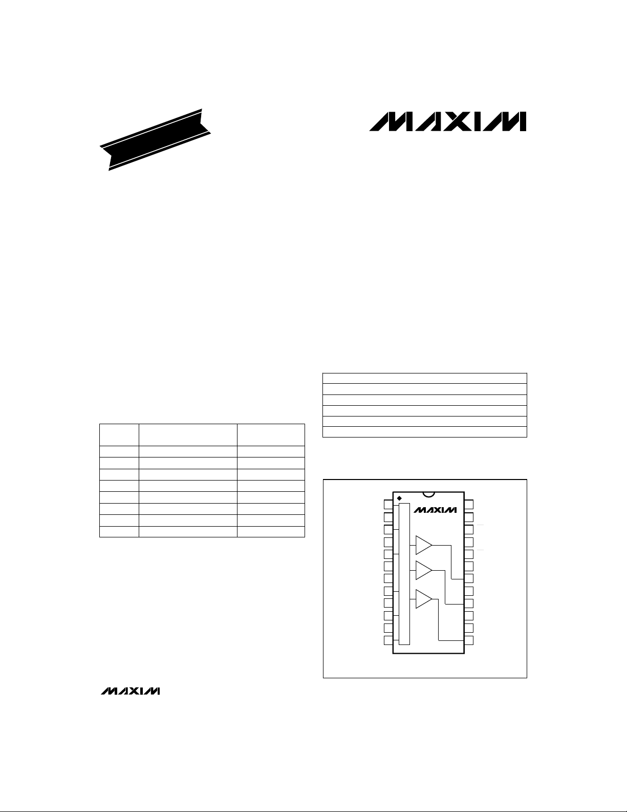
_________________Pin Configurations
TOP VIEW
IN0A
IN1A
IN2A
IN0B
IN1B
IN2B
0°C to +70°C 24 Narrow Plastic DIP
-40°C to +85°C
= +25°C, DC parameters only.
A
1
GND
GND
GND
GND
2
3
4
5
V-
6
V-
7
8
9
10
11
12
MAX463
MAX465
3P2T SWITCH
24
GND
23
LE
22
EN
21
A0
20
CS
19
V-
18
OUT0
17
V+
16
OUT1
15
GND
14
V+
13
OUT2
MAX463–MAX470
Typical Operating Circuit appears at end of data sheet.
________________________________________________________________
Pin Configurations continued at end of data sheet.
DIP/SO
Maxim Integrated Products
Call toll free 1-800-998-8800 for free samples or literature.
1
Two-Channel, Triple/Quad
RGB Video Switches and Buffers
ABSOLUTE MAXIMUM RATINGS
Power-Supply Ranges
V+ to V- ................................................................................12V
Analog Input Voltage..........................(V- - 0.3V) to (V+ + 0.3V)
Digital Input Voltage...................................-0.3V to (V+ + 0.3V)
Output Short-Circuit Duration (to GND)........................1 Minute
Input Current into Any Pin, Power On or Off...................±50mA
Continuous Power Dissipation (T
16-Pin Plastic DIP (derate 22.22mW/°C above +70°C)....1778mW
16-Pin Wide SO (derate 20.00mW/°C above +70°C) .......1600mW
Stresses beyond those listed under “Absolute Maximum Ratings” may cause permanent damage to the device. These are stress ratings only, and functional
operation of the device at these or any other conditions beyond those indicated in the operational sections of the specifications is not implied. Exposure to
absolute maximum rating conditions for extended periods may affect device reliability.
= +70°C)
A
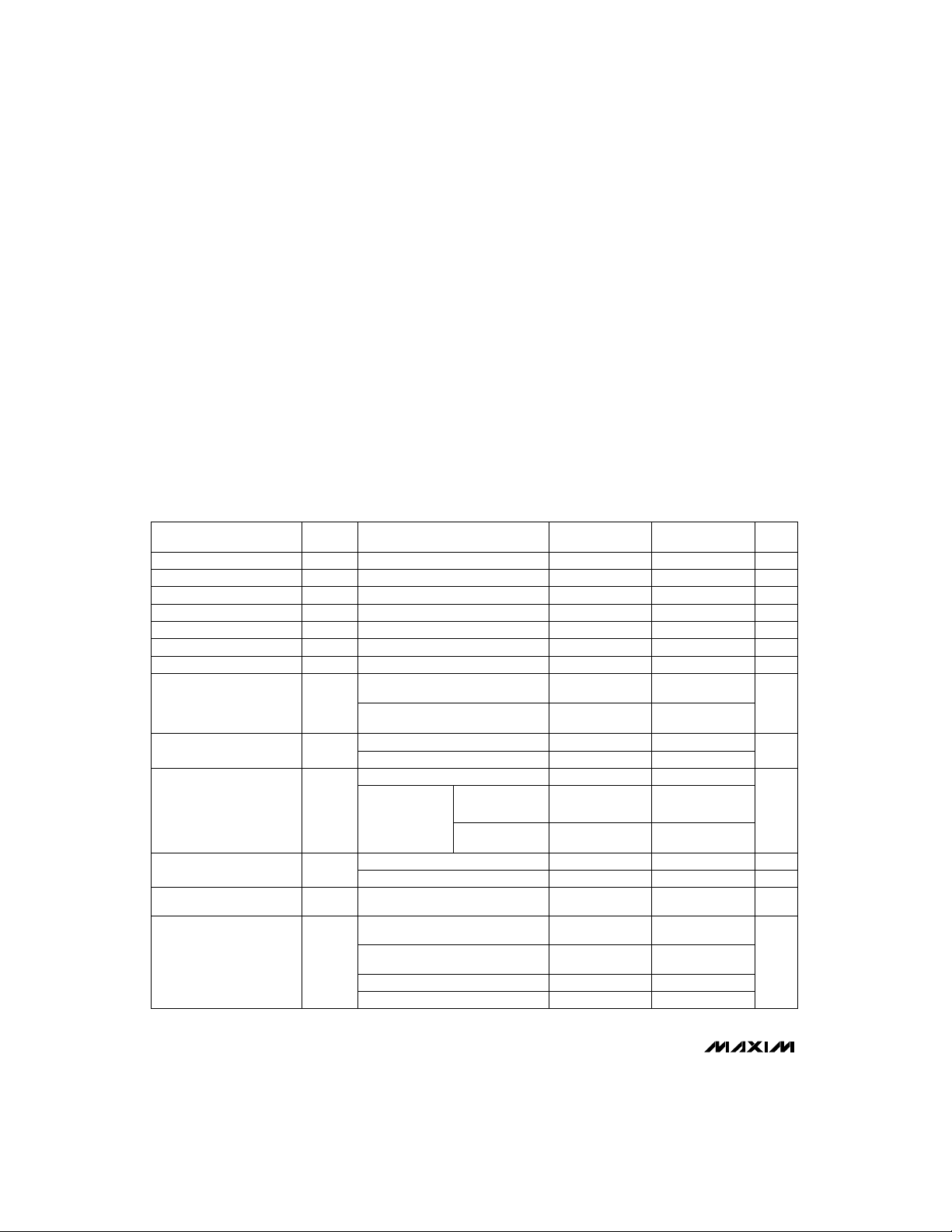
ELECTRICAL CHARACTERISTICS
(V+ = 5V, V- = -5V, -2V ≤ VIN≤ +2V, R
MAX463–MAX470
PARAMETER SYMBOL UNITS
Operating Supply Voltage V
Input Voltage Range
Offset Voltage V
Power-Supply Rejection Ratio PSRR 50 60 dB
On Input Bias Current I
On Input Resistance R
Input Capacitance C
Voltage-Gain Accuracy
Output Voltage Swing V
Output Impedance R
Output Resistance,
Disabled Mode
Output Capacitance,
Disabled Mode
Positive Supply Current I+
R
C
= 75Ω, unless otherwise noted.)
LOAD
CONDITIONS
S
V
IN
OS
BIAS
IN
Channel off or on
IN
MAX463/MAX464, MAX467/MAX468
(Note 1)
MAX465/MAX466, MAX469/MAX470,
R
= 150Ω, (Note 2)
LOAD
R
= 150Ω
OUT
OUT
OUTD
OUTD
LOAD
R
= 75Ω
LOAD
fIN= 10MHz
fIN= DC
MAX463/MAX464
MAX465/MAX466
MAX463–MAX466
MAX463/MAX465/MAX467/MAX469,
VIN= 0V
MAX464/MAX466/MAX468/MAX470,
VIN= 0V
MAX463/MAX465, disabled mode
MAX464/MAX466, disabled mode
24-Pin Narrow Plastic DIP
(derate 20.2mW/°C above +70°C)..................................1620mW
24-Pin Wide SO (derate 19.3mW/°C above +70°C) .........1590mW
28-Pin Narrow Plastic DIP
(derate 20.2mW/°C above +70°C)..................................1620mW
28-Pin Wide SO (derate 18.1mW/°C above +70°C) .........1440mW
Operating Temperature Ranges
MAX4_ _C_ _.........................................................0°C to +70°C
MAX4_ _E_ _......................................................-40°C to +85°C
Storage Temperature Range.............................-65°C to +150°C
Lead Temperature (soldering, 10sec).............................+300°C
MAX463/MAX464,
MAX467/MAX468
MAX465/MAX466,
MAX469/MAX470
TA= +25°C
MIN TYP MAX
±4.75 ±5 ±5.25 V
-2 2 V
±3 ±10 mV±15
±1 ±3 µA
300 700 kΩ
5 pF
0.2 0.5
0.3 1.0
±2.5 ±2.8
±2.0 ±2.4
5
0.05
0.1
150 250 kΩ
0.7 1 kΩ
10 pF
65 80
85 100
35 45
40 50
TA= T
to T
MIN
MIN MAX
±4.75 ±5.25
-2 2
50
150
±2.5
-1.5/+2
100
0.7
MAX
±5
1.0
2.0
100
120
50
55
%
V
Ω
mA
2 _______________________________________________________________________________________
Two-Channel, Triple/Quad
RGB Video Switches and Buffers
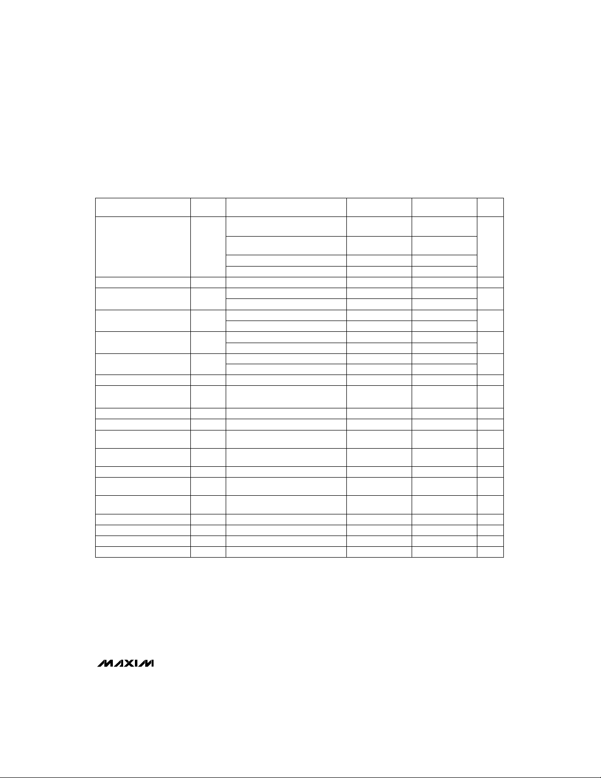
ELECTRICAL CHARACTERISTICS (continued)
(V+ = 5V, V- = -5V, -2V ≤ VIN≤ +2V, R
PARAMETER
Negative Supply Current
Input Noise Density en 20 nV/√–H—z
-3dB Bandwidth BW
Differential Gain Error
(Note 3)
Differential Phase Error
(Note 3)
Settling Time to 0.1%
Adjacent Channel Crosstalk
(Note 4)
All-Hostile Crosstalk (Note 5) XTALK 50 dB
All-Hostile Off Isolation (Note 6)
Channel Switching
Propagation Delay (Note 7)
Channel Switching Time
(Note 8)
Switching Transient 300 mV
Amplifier Switching Off-Time
(Note 9)
Amplifier Switching On-Time
(Note 10)
Logic Input High Threshold V
Logic Input Low Threshold V
Logic Input Current High I
Logic Input Current Low I
SYMBOL
XTALK
= 75Ω, unless otherwise noted.)
LOAD
CONDITIONS
MAX463/MAX465/MAX467/MAX469,
VIN= 0V
MAX464/MAX466/MAX468/MAX470,
I-
VIN= 0V
MAX463/MAX465, disabled mode
MAX464/MAX466, disabled mode
fIN= 10kHz
MAX463/MAX464, MAX467/MAX468
SR
MAX465/MAX466, MAX469/MAX470
MAX463/MAX464, MAX467/MAX468
MAX465/MAX466, MAX469/MAX470
MAX463/MAX464, MAX467/MAX468
DG
MAX465/MAX466, MAX469/MAX470
MAX463/MAX464, MAX467/MAX468
DP
MAX465/MAX466, MAX469/MAX470
t
VIN= 2V-to-0V step
S
fIN= 10MHz
fIN= 10MHz
ISO
fIN= 10MHz, MAX463–MAX466
t
MAX463–MAX466
PD
t
MAX463–MAX466
SW
V
= V
INA
t
MAX463–MAX466
OFF
t
ON
E—N–, A0, C—S–, LE; MAX463–MAX466
IH
E—N–, A0, C—S–, LE; MAX463–MAX466
IL
INHI
INLO
= 0V, MAX463–MAX466
INB
TA= +25°C
MIN TYP MAX
50 65
65 80
20 30
25 35
200
300
100
90
0.01
0.12
0.03
0.14
50 ns
60
70
15 ns
20 ns
80 ns
100 nsMAX463–MAX466
0.8 V
TA= T
2 V
200 µAE—N–, A0, C—S–, LE; MAX463–MAX466 200
200 µAE—N–, A0, C—S–, LE; MAX463–MAX466 200
to T
MIN
MIN MAX
75
95
35
40
2
0.8
MAX
UNITS
V/µsSlew Rate
MHz
deg.
MAX463–MAX470
mA
%
dB
dB
P-P
_______________________________________________________________________________________ 3
Two-Channel, Triple/Quad
RGB Video Switches and Buffers
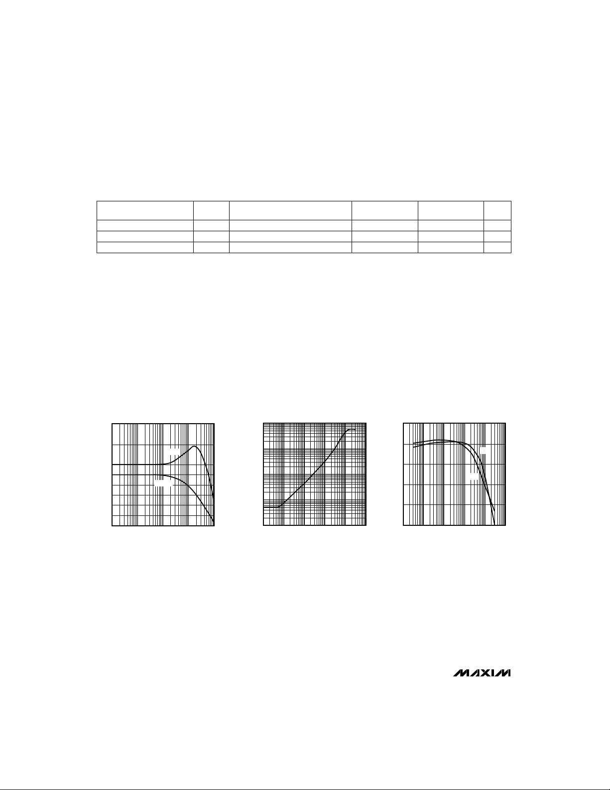
ELECTRICAL CHARACTERISTICS (continued)
(V+ = 5V, V- = -5V, -2V ≤ VIN≤ +2V, R
PARAMETER
SYMBOL UNITS
Address Setup Time (Note 11) t
Address Hold Time (Note 11) t
C—S–Pulse Width Low (Note 11) t
Note 1: Voltage gain accuracy for the unity-gain devices is defined as [(V
Note 2: Voltage gain accuracy for the gain-of-two devices is defined as [(V
Note 3: Tested with a 3.58MHz sine wave of amplitude 40IRE superimposed on a linear ramp (0IRE to 100IRE), R
Note 4: Tested with the selected input connected to ground through a 75Ω resistor, and a 4V
Note 5: Tested in the same manner as described in Note 4, but with all other inputs driven.
Note 6: Tested with LE = 0V, E—N–= V+, and all inputs driven with a 4V
Note 7: Measured from a channel switch command to measurable activity at the output.
Note 8: Measured from where the output begins to move to the point where it is well defined.
Note 9: Measured from a disable command to amplifier in a non-driving state.
MAX463–MAX470
Note 10: Measured from an enable command to the point where the output reaches 90% current out.
Note 11: Guaranteed by design.
__________________________________________Typical Operating Characteristics
(TA = +25°C, unless otherwise noted.)
= 75Ω, unless otherwise noted.)
LOAD
CONDITIONS
SU
H
CS
MIN TYP MAX
30 nsE—N–, A0, C—S–, LE; MAX463–MAX466 30
15 nsE—N–, A0, C—S–, LE; MAX463–MAX466 15
- VIN) at VIN= 1V - (V
OUT
/2 - VIN) at VIN= 1V - (V
OUT
, 10MHz sine wave.
P-P
T
A
= +25°C
TA= T
to T
MIN
MIN MAX
MAX
0 nsE—N–, A0, C—S–, LE; MAX463–MAX466 0
- VIN) at VIN= -1V]/2.
OUT
/2 - VIN) at VIN= -1V]/2.
OUT
= 150Ω to ground.
sine wave at 10MHz driving adjacent input.
P-P
L
GAIN AND PHASE RESPONSES
2
1
0
GAIN (dB)
–1
–2
–3
10k 100k
FREQUENCY (Hz)
MAX468
GAIN
PHASE
1M 100M
10M
MAX463/470 -01
0
36
72
108
144
PHASE (DEGREES)
180
OUTPUT IMPEDANCE
100
Ω
10
1
OUTPUT IMPEDANCE ( )
0.1
0.01
vs. FREQUENCY
FREQUENCY (Hz)
MAX464
1M 100M
10M10k
MAX463/470 -02
1G100k
POWER-SUPPLY REJECTION RATIO
60
50
40
PSRR (dB)
30
20
10
1k 100k
vs. FREQUENCY
FREQUENCY (Hz)
4 _______________________________________________________________________________________
MAX468
1M 100M
MAX463/470 -03
V–
V+
10M10k
Two-Channel, Triple/Quad
RGB Video Switches and Buffers
____________________________Typical Operating Characteristics (continued)
(TA = +25°C, unless otherwise noted.)
VOLTAGE GAIN ACCURACY
0.16
0.14
0.12
0.10
PERCENTAGE (%)
0.08
0.06
30
25
20
15
10
5
SUPPLY CURRENT PER AMPLIFIER (mA)
0
–50
vs. TEMPERATURE
MAX465
MAX463
–25 0 5025 75–50
TEMPERATURE (°C)
SUPPLY CURRENT PER AMPLIFIER
vs. TEMPERATURE
I+
I–
–25 0 50
25 75
TEMPERATURE (°C)
MAX463/470 -04
100
MAX463/470 -09
100
DISABLED OUTPUT RESISTANCE
vs. TEMPERATURE
400
350
300
250
OUTPUT RESISTANCE (kΩ)
200
–25 0 5025 75–50
TEMPERATURE (°C)
DISABLED SUPPLY CURRENT
40
35
30
25
20
SUPPLY CURRENT (mA)
15
10
–50
vs. TEMPERATURE
I+
I–
–25 0 50
TEMPERATURE (°C)
MAX463
25 75
MAX463/470 -05
100
MAX463/470 -07
100
DISABLED OUTPUT RESISTANCE
1.30
1.25
1.20
1.15
OUTPUT RESISTANCE (kΩ)
1.10
4
3
2
1
0
–1
OUTPUT VOLTAGE (V)
–2
–3
–4
10 100
MAX465
vs. TEMPERATURE
–25 0 5025 75–50
TEMPERATURE (°C)
OUTPUT VOLTAGE SWING
vs. LOAD RESISTANCE
MAX463/4/7/8:VIN = 4V
MAX465/6/9/70:V
LOAD RESISTANCE ( )
1000 10000
= 2V
IN
Ω
MAX463–MAX470
MAX463/470 -06
100
MAX463/470 -08
_______________________________________________________________________________________
5
 Loading...