

Page 1
For free samples & the latest literature: http://www.maxim-ic.com, or phone 1-800-998-8800.
For small orders, phone 1-800-835-8769.
General Description
The MAX4661/MAX4662/MAX4663 quad analog switches
feature low on-resistance of 2.5Ω max. On-resistance is
matched between switches to 0.5Ω max and is flat
(0.5Ω max) over the specified signal range. Each
switch can handle Rail-to-Rail®analog signals. Offleakage current is only 5nA max at TA= +85°C. These
analog switches are ideal in low-distortion applications
and are the preferred solution over mechanical relays in
automatic test equipment or applications where current
switching is required. They have lower power requirements, use less board space, and are more reliable
than mechanical relays.
The MAX4661 has four normally closed (NC) switches,
and the MAX4662 has four normally open (NO) switches.
The MAX4663 has two NC and two NO switches, and features guaranteed break-before-make switching.
These devices operate from a single +4.5V to +36V supply or from dual ±4.5V to ±20V supplies. A separate logic
supply pin guarantees TTL/CMOS-logic compatibility
when operating across the entire supply voltage range.
Applications
Reed Relay Replacement Avionics
Test Equipment ADC Systems
Communication Systems Sample-and-Hold Circuits
PBX, PABX Systems Data Acquisition Systems
Audio-Signal Routing
Features
♦ Low On-Resistance (2.5Ω max)
♦ Guaranteed R
ON
Match Between Channels
(0.5Ω max)
♦ Guaranteed R
ON
Flatness over Specified Signal
Range (0.5Ω max)
♦ Rail-to-Rail Signal Handling
♦ Guaranteed Break-Before-Make (MAX4663)
♦ > 2kV ESD Protection per Method 3015.7
♦ +4.5V to +36V Single-Supply Operation
±4.5V to ±20V Dual-Supply Operation
♦ TTL/CMOS-Compatible Control Inputs
MAX4661/MAX4662/MAX4663
2.5Ω, Quad, SPST,
CMOS Analog Switches
________________________________________________________________
Maxim Integrated Products
1
19-1516; Rev 0; 7/99
PART
MAX4661CAE
MAX4661CWE
MAX4661CPE 0°C to +70°C
0°C to +70°C
0°C to +70°C
TEMP. RANGE PIN-PACKAGE
16 SSOP
16 Wide SO
16 Plastic DIP
Ordering Information continued at end of data sheet.
Ordering Information
MAX4661EAE -40°C to +85°C 16 SSOP
MAX4661EWE -40°C to +85°C 16 Wide SO
MAX4661EPE -40°C to +85°C 16 Plastic DIP
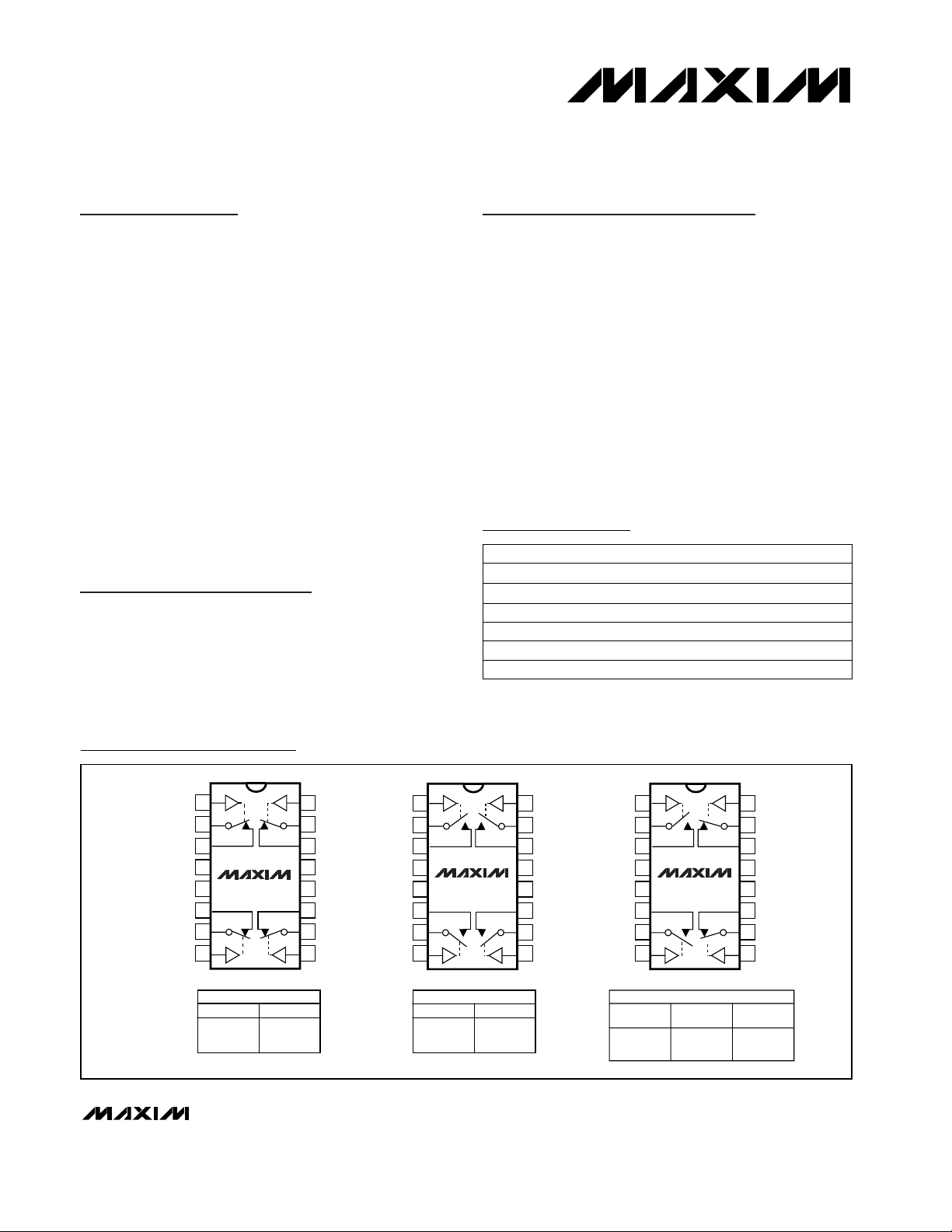
SWITCHES SHOWN FOR LOGIC “0” INPUT
SSOP/SO/DIP
MAX4662
LOGIC SWITCH
0
1
OFF
ON
TOP VIEW
SSOP/SO/DIP
MAX4661
LOGIC SWITCH
0
1
ON
OFF
SSOP/SO/DIP
MAX4663
LOGIC
SWITCHES
1, 4
0
1
OFF
ON
SWITCHES
2, 3
ON
OFF
16
15
14
13
12
11
10
9
1
2
3
4
5
6
7
8
IN2
COM2
NC2
V+
V-
NO1
COM1
IN1
MAX4663
V
L
NC3
COM3
IN3
IN4
COM4
NO4
GND
16
15
14
13
12
11
10
9
1
2
3
4
5
6
7
8
IN2
COM2
NC2
V+
V-
NC1
COM1
IN1
MAX4661
V
L
NC3
COM3
IN3
IN4
COM4
NC4
GND
16
15
14
13
12
11
10
9
1
2
3
4
5
6
7
8
IN2
COM2
NO2
V+
V-
NO1
COM1
IN1
MAX4662
V
L
NO3
COM3
IN3
IN4
COM4
NO4
GND
Pin Configurations/Functional Diagrams/Truth Tables
Rail-to-Rail is a registered trademark of Nippon Motorola, Ltd.
Page 2
MAX4661/MAX4662/MAX4663
2.5Ω, Quad, SPST,
CMOS Analog Switches
2 _______________________________________________________________________________________
ABSOLUTE MAXIMUM RATINGS
Stresses beyond those listed under “Absolute Maximum Ratings” may cause permanent damage to the device. These are stress ratings only, and functional
operation of the device at these or any other conditions beyond those indicated in the operational sections of the specifications is not implied. Exposure to
absolute maximum rating conditions for extended periods may affect device reliability.
V+ to GND..............................................................-0.3V to +44V
V- to GND ..............................................................+0.3V to -44V
V+ to V-...................................................................-0.3V to +44V
V
L
to GND .......................................(GND - 0.3V) to (V+ + 0.3V)
All Other Pins to GND (Note 1).............(V- - 0.3V) to (V+ + 0.3V)
Continuous Current (COM_, NO_, NC_) ........................±200mA
Peak Current (COM_, NO_, NC_)
(pulsed at 1ms, 10% duty cycle)................................ ±300mA
Continuous Power Dissipation (T
A
= +70°C)
SSOP (derate 7.1mW/°C above +70°C) .......................571mW
Wide SO (derate 9.52mW/°C above +70°C).................762mW
Plastic DIP (derate 10.53mW/°C above +70°C) ...........842mW
Operating Temperature Ranges
MAX466_C_E ......................................................0°C to +70°C
MAX466_E_E ....................................................-40°C to +85°C
Storage Temperature Range .............................-65°C to +150°C
Lead Temperature (soldering, 10sec) .............................+300°C
-5 5
-5 5
-20 20
TA= T
MIN
to T
MAX
V
TA= +25°C
V- V+
V
COM_,
V
NO_,VNC_
Input Voltage Range (Note 3)
IN_ = 0.8V, all others = 2.4V
IN_ = 2.4V, all others = 0.8V
I
COM_
= 10mA,
V
NO_
or V
NC_
= ±10V
TA= +25°C
TA= +25°C
TA= +25°C
CONDITIONS
0.8V
IN_L
Logic Input Voltage Low
Ω
0.1 0.5
∆R
ON
COM_ to NO_ or NC_
On-Resistance Match Between
Channels (Notes 3, 4)
Ω
1.7 2.5
R
ON
COM_ to NO or NC_
On-Resistance
V2.4V
IN_H
Logic Input Voltage High
-0.5 0.001 0.5I
IN_L
Input Current with Input Voltage
Low
µA-0.5 0.001 0.5I
IN_H
Input Current with Input Voltage
High
Ω
0.1 0.5
R
FLAT(ON)
COM_ to NO_ or NC_
On-Resistance Flatness
(Notes 3, 5)
nA
-0.5 0.01 0.5
I
NO_, INC_
Off-Leakage Current
(NO_ or NC_) (Note 6)
nA
-0.5 0.01 0.5
I
COM_(OFF)
COM Off-Leakage Current
(Note 6)
nA
-1 0.01 1
I
COM_(ON)
COM On-Leakage Current
(Note 6)
UNITSMIN TYP MAXSYMBOLPARAMETER
I
COM_
= 10mA,
V
NO_
or V
NC_
= ±10V
I
COM_
= 10mA; V
NO_
or V
NC_
= -5V, 0, 5V
TA= +25°C
V
COM_
= ±10V,
V
NO_
or V
NC_
=
–
+
10V
V
COM_
= ±10V,
V
NO_
or V
NC_
=
–
+
10V
V
COM_
= ±10V,
V
NO_
or V
NC_
= ±10V
or floating
TA= +25°C
TA= T
MIN
to T
MAX
2.7
0.6
TA= T
MIN
to T
MAX
0.6
TA= T
MIN
to T
MAX
TA= T
MIN
to T
MAX
TA= T
MIN
to T
MAX
ELECTRICAL CHARACTERISTICS—Dual Supplies
(V+ = +15V, V- = -15V, VL= +5V, V
IN_H
= +2.4V, V
IN_L
= +0.8V, TA = T
MIN
to T
MAX
, unless otherwise noted. Typical values are at
T
A
= +25°C.) (Note 2)
µA
V
ANALOG SWITCH
LOGIC INPUT
Note 1: Signals on NC_, NO_, COM_, or IN_ exceeding V+ or V- will be clamped by internal diodes. Limit forward diode current to maximum
current rating.
Page 3
MAX4661/MAX4662/MAX4663
2.5Ω, Quad, SPST,
CMOS Analog Switches
_______________________________________________________________________________________ 3
VIN= 0 or 5V µA
TA= +25°C
-0.5 0.001 0.5
I+Positive Supply Current
TA= +25°C
f = 1MHz, Figure 7
RL= 50Ω, CL = 5pF, f = 1MHz,
Figure 6
TA= T
MIN
to T
MAX
-5 5
RL= 50Ω, CL = 5pF, f = 1MHz,
Figure 5
V
COM_
= ±10V, Figure 3, TA= +25°C
VIN= 0 or 5V
TA= +25°C
f = 1MHz, Figure 7
CONDITIONS
V±4.5 ±20.0Power-Supply Range
pF
dB
f = 1MHz, Figure 8 pF250C
COM
On-Capacitance
55C
COM
COM_ Off-Capacitance
-0.5 0.001 0.5
I
L
Logic Supply Current
-0.5 0.001 0.5
I-Negative Supply Current
pFC
OFF
NC_ or NO_ Capacitance
-59V
CT
Crosstalk (Note 8)
dB-56V
ISO
Off-Isolation (Note 7)
ns530t
OPEN
Break-Before-Make Time
(MAX4663 only)
-0.5 0.001 0.5
I
GND
Ground Current
130 275
100 175
UNITSMIN TYP MAXSYMBOLPARAMETER
VIN= 0 or 5V
VIN= 0 or 5V
TA= +25°C
TA= T
MIN
to T
MAX
-5 5
-5 5
TA= T
MIN
to T
MAX
-5 5
ELECTRICAL CHARACTERISTICS—Dual Supplies (continued)
(V+ = +15V, V- = -15V, VL= +5V, V
IN_H
= +2.4V, V
IN_L
= +0.8V, TA = T
MIN
to T
MAX
, unless otherwise noted. Typical values are at
T
A
= +25°C.) (Note 2)
µA
µA
µA
TA= T
MIN
to T
MAX
55
ns
400
t
ON
Turn-On Time
V
COM_
= ±10V,
Figure 2
ns
300
t
OFF
Turn-Off Time
V
COM_
= ±10V,
Figure 2
CL = 1.0nF, V
GEN
= 0, R
GEN
= 0,
Figure 4
pC300QCharge Injection
POWER SUPPLY
SWITCH DYNAMIC CHARACTERISTICS
TA= +25°C
TA= T
MIN
to T
MAX
TA= +25°C
TA= T
MIN
to T
MAX
Page 4
MAX4661/MAX4662/MAX4663
2.5Ω, Quad, SPST,
CMOS Analog Switches
4 _______________________________________________________________________________________
-5 5
-5 5
-20 20
TA= T
MIN
to T
MAX
V
TA= +25°C
GND V+
V
COM_,VNO_,
V
NC_
Input Voltage Range (Note 3)
IN_ = 0.8V, all others = 2.4V
+4.5 +36.0
IN_ = 2.4V, all others = 0.8V
I
COM_
= 10mA,
V
NO_
or V
NC_
= 10V
TA= +25°C
TA= +25°C
TA= +25°C
CONDITIONS
Power-Supply Range
VIN= 0 or 5V
VIN= 0 or 5V
-0.5 0.001 0.5
I
L
Logic Supply Current
µA
-0.5 0.001 0.5
I+Positive Supply Current
V
µA
VIN= 0 or 5V
-0.5 0.001 0.5
I
GND
Ground Current µA
TA= +25°C
TA= +25°C
TA= T
MIN
to T
MAX
TA= +25°C
TA= T
MIN
to T
MAX
TA= T
MIN
to T
MAX
-5 5
-5 5
-5 5
0.8V
IN_L
Logic Input Voltage Low
Ω
0.03 0.4
∆R
ON
COM_ to NO_ or NC_
On-Resistance Match Between
Channels (Notes 3, 4)
Ω
34
R
ON
COM_ to NO or NC_
On-Resistance
V2.4V
IN_H
Logic Input Voltage High
-0.5 0.001 0.5I
IN_L
Input Current with Input Voltage
Low
µA-0.5 0.001 0.5I
IN_H
Input Current with Input Voltage
High
Ω
0.1 0.7
R
FLAT(ON)
COM_ to NO_ or NC_
On-Resistance Flatness
(Notes 3, 5)
nA
-0.5 0.01 0.5
I
NO_
I
NC_
Off-Leakage Current
(NO_ or NC_) (Notes 6, 9)
nA
-0.5 0.01 0.5
I
COM_(OFF)
COM Off-Leakage Current
(Notes 6, 9)
nA
-1 0.01 1
I
COM_(ON)
COM On-Leakage Current
(Notes 6, 9)
UNITSMIN TYP MAXSYMBOLPARAMETER
I
COM_
= 10mA,
V
NO_
or = V
NC_
= 10V
I
COM_
= 10mA; V
NO_
or V
NC_
= 3V, 6V, 9V
TA= +25°C
V
COM_
= 1V, 10V;
V
NO_
or V
NC_
= 10V,
1V
V
NO_
or V
NC_
= 10V,
1V; V
COM_
= 1V, 10V
V
COM_
= 1V ,10V;
V
NO_
or V
NC_
= 1V,
10V, or floating
TA= +25°C
TA= T
MIN
to T
MAX
5
0.5
TA= T
MIN
to T
MAX
0.8
TA= T
MIN
to T
MAX
TA= T
MIN
to T
MAX
TA= T
MIN
to T
MAX
ELECTRICAL CHARACTERISTICS—Single Supply
(V+ = +12V, V- = 0, VL= +5V, V
IN_H
= +2.4V, V
IN_L
= +0.8V, TA = T
MIN
to T
MAX
, unless otherwise noted. Typical values are at
T
A
= +25°C.) (Note 2)
µA
V
ANALOG SWITCH
LOGIC INPUT
POWER SUPPLY
Page 5

MAX4661/MAX4662/MAX4663
2.5Ω, Quad, SPST,
CMOS Analog Switches
_______________________________________________________________________________________ 5
ELECTRICAL CHARACTERISTICS—Single Supply (continued)
(V+ = +12V, V- = 0, VL= +5V, V
IN_H
= +2.4V, V
IN_L
= +0.8V, TA = T
MIN
to T
MAX
, unless otherwise noted. Typical values are at
T
A
= +25°C.) (Note 2)
Note 2: The algebraic convention, where the most negative value is a minimum and the most positive value a maximum, is used in
this data sheet.
Note 3: Guaranteed by design.
Note 4: ∆R
ON
= R
ON(MAX)
- R
ON(MIN)
.
Note 5: Flatness is defined as the difference between the maximum and minimum value of on-resistance as measured over the
specified analog signal range.
Note 6: Leakage parameters are 100% tested at maximum-rated hot temperature and guaranteed by correlation at +25°C.
Note 7: Off-isolation = 20log
10
[V
COM
/ (VNCor VNO)], V
COM
= output, VNCor VNO= input to off switch.
Note 8: Between any two switches.
Note 9: Leakage testing at single supply is guaranteed by testing with dual supplies.
200 400
f = 1MHz, Figure 8On-Capacitance C
COM
140 pF
f = 1MHz, Figure 7COM Off-Capacitance C
COM
85 pF
f = 1MHz, Figure 7NC_ or NO_ Capacitance C
OFF
85 pF
RL= 50Ω, CL = 5pF, f = 1MHz,
Figure 6
V
COM_
= 10V, Figure 3, TA= +25°C
PARAMETER SYMBOL MIN TYP MAX UNITS
Crosstalk (Note 8) V
CT
-60 dB
Break-Before-Make Time
(MAX4663 only) (Note 3)
t
OPEN
5 125 ns
100 250
CONDITIONS
Turn-On Time (Note 3) t
ON
500
ns
V
COM_
= 10V,
Figure 2
V
COM_
= 10V,
Figure 2
Turn-Off Time (Note 3) t
OFF
350
ns
TA= +25°C
TA= T
MIN
to T
MAX
TA= +25°C
TA= T
MIN
to T
MAX
CL = 1.0nF, V
GEN
= 0, R
GEN
= 0,
Figure 4
Charge Injection Q 20 pC
SWITCH DYNAMIC CHARACTERISTICS
Page 6

MAX4661/MAX4662/MAX4663
2.5Ω, Quad, SPST,
CMOS Analog Switches
6 _______________________________________________________________________________________
Typical Operating Characteristics
(TA = +25°C, unless otherwise noted.)
0
1.0
0.5
2.0
1.5
3.0
2.5
3.5
4.5
4.0
5.0
-20 -10 -5-15 0 5 10 15 20
ON-RESISTANCE vs. V
COM
(DUAL SUPPLIES)
MAX4661/2/3-01
V
COM
(V)
R
ON
(Ω)
V+, V- = ±5V
V+, V- = ±15V
V+, V- = ±20V
0
0.50
0.25
1.00
0.75
1.50
1.25
1.75
2.25
2.00
2.50
-10 -5-15 0 5 10 15
ON-RESISTANCE vs. V
COM
AND
TEMPERATURE (DUAL SUPPLIES)
MAX4661/2/3-02
V
COM
(V)
R
ON
(Ω)
TA = +85°C
TA = +25°C
V+, V- = ±15V
T
A
= -40°C
0
3
2
1
4
5
6
7
8
9
10
084 121620242106 141822
ON-RESISTANCE vs. V
COM
(SINGLE SUPPLY)
MAX4661/2/3-03
V
COM
(V)
R
ON
(Ω)
V+ = 5V
V+ = 12V
V+ = 24V
0
1.50
1.00
0.50
2.00
2.50
3.50
3.00
4.00
0231 456789101112
ON-RESISTANCE vs. V
COM
AND
TEMPERATURE (SINGLE SUPPLY)
MAX4661/2/3-04
V
COM
(V)
R
ON
(Ω)
TA = +85°C
TA = +25°C
TA = -40°C
V+ = +12V
V- = GND
0.1m
0.01
1m
10
1
0.1
1k
10k
100
100k
-40 20-20 0 40 60 80 100
ON/OFF-LEAKAGE CURRENT
vs. TEMPERATURE
MAX4661/2/3-05
TEMPERATURE (°C)
LEAKAGE (pA)
ON-LEAKAGE
OFF-LEAKAGE
V+ = +15V
V- = -15V
-200
0
-100
200
100
300
400
-20 -5 0-10-15 5 10 15 20
CHARGE INJECTION
vs. V
COM
MAX4661/2/3-06
V
COM
(V)
Q (pC)
V- = -15V
V+ = +15V
V- = GND
V+ = 12V
0.1
I+
I-
0.01
0.001
100
10
1
10k
100k
1k
-40 20-20 0 40 60 80 100
POWER-SUPPLY CURRENT
vs. TEMPERATURE
MAX4661/2/3-07
TEMPERATURE (°C)
I+, I- (nA)
V+ = +15V
V- = -15V
-10
-100
0.1 100101
FREQUENCY RESPONSE
-70
-90
-30
-50
0
-60
-80
-20
-40
MAX4661/2/3-08
FREQUENCY (MHz)
LOSS (dB)
90
180
-720
-450
-630
-90
-270
-360
-540
-0
-180
PHASE (degrees)
OFF-ISOLATION
ON-PHASE
ON-RESPONSE
V+ = +15V
V- = -15V
INPUT = OdBm
50Ω IN AND OUT
Page 7

MAX4661/MAX4662/MAX4663
2.5Ω, Quad, SPST,
CMOS Analog Switches
_______________________________________________________________________________________ 7
NAME FUNCTION
MAX4661
1, 16, 9, 8
IN1, IN2,
IN3, IN4
Logic-Control Digital Inputs
2, 15,
10, 7
COM1, COM2,
COM3, COM4
Analog Switch Common Terminals
3, 14, 11, 6
NC1, NC2,
NC3, NC4
Analog Switch Normally Closed Terminals
4 V-
Negative Analog Supply-Voltage Input. Connect to GND for singlesupply operation.
— NC2, NC3 Analog Switch Normally Closed Terminals
— NO1, NO4 Analog Switch Normally Open Terminals
—
NO1, NO2,
NO3, NO4
Analog Switch Normally Open Terminals
13 V+ Positive Analog Supply Input
12 V
L
Logic-Supply Input
5 GND Ground
Pin Description
MAX4662
1, 16, 9, 8
2, 15,
10, 7
—
4
—
—
3, 14, 11, 6
13
12
5
MAX4663
1, 16, 9, 8
PIN
2, 15,
10, 7
—
4
14, 11
3, 6
—
13
12
5
Applications Information
Overvoltage Protection
Proper power-supply sequencing is recommended for
all CMOS devices. Do not exceed the absolute maximum ratings because stresses beyond the listed ratings can cause permanent damage to the devices.
Always sequence V+ on first, then V-, followed by the
logic inputs, NO, or COM. If power-supply sequencing
is not possible, add two small-signal diodes (D1, D2)
in series with the supply pins and a Schottky diode
between V+ and VLfor overvoltage protection (Figure
1). Adding diodes reduces the analog signal range to
one diode drop below V+ and one diode drop above V-,
but does not affect the devices’ low switch resistance
and low leakage characteristics. Device operation is
unchanged, and the difference between V+ and Vshould not exceed 44V.
Off-Isolation at High Frequencies
In 50Ω systems, the high-frequency on-response of
these parts extends from DC to above 100MHz with a
typical loss of -2dB. When the switch is turned off, however, it behaves like a capacitor and off-isolation
decreases with increasing frequency. (Above 300MHz,
the switch actually passes more signal turned off than
turned on.) This effect is more pronounced with higher
source and load impedances.
Above 5MHz, circuit board layout becomes critical and
it becomes difficult to characterize the response of the
switch independent of the circuit. The graphs shown in
the
Typical Operating Characteristics
were taken using
a 50Ω source and load connected with BNC connectors to a circuit board deemed “average”; that is,
designed with isolation in mind, but not using stripline
or other special RF circuit techniques. For critical applications above 5MHz, use the MAX440, MAX441, and
MAX442, which are fully characterized up to 160MHz.
COM_
V-
V+
V
L
NO_
* INTERNAL PROTECTION DIODES
D2
D1
-15V
+15V
MAX4661
MAX4662
MAX4663
*
*
*
*
Figure 1. Overvoltage Protection Using External Blocking
Diodes
Page 8

MAX4661/MAX4662/MAX4663
2.5Ω, Quad, SPST,
CMOS Analog Switches
8 _______________________________________________________________________________________
Figure 3. Break-Before-Make Interval (MAX4663 only)
Figure 2. Switching-Time Test Circuit
t
OFF
tr < 20ns
tf < 20ns
0.9V
0
+3V
LOGIC
INPUT
SWITCH
OUTPUT
0
0
50%
V
O
0.9V
t
ON
LOGIC INPUT WAVEFORMS INVERTED FOR SWITCHES
THAT HAVE THE OPPOSITE LOGIC SENSE.
0
SWITCH
INPUT
LOGIC
INPUT
+5V
V
L
V
COM_
COM_
IN_
GND
0
REPEAT TEST FOR EACH SWITCH. FOR LOAD
CONDITIONS, SEE
INCLUDES FIXTURE AND STRAY CAPACITANCE.
C
L
V
= V
O
COM (
RL + R
Electrical Characteristics.
R
L
)
ON
+15V
V+
NO_
OR NC_
V-
-15V
MAX4661
MAX4662
MAX4663
R
L
100Ω
SWITCH
OUTPUT
C
L
35pF
V
O
MAX4663
V
V
LOGIC
INPUT
COM1
COM1
COM2
COM2
IN1, 2
GND
C
INCLUDES FIXTURE AND STRAY CAPACITANCE.
L
+15V
-15V
V+
NO
NC
V-
V
OUT2
R
C
L2
L2
R
= 100Ω
L
= 35pF
C
L
V
OUT1
R
C
L1
L1
LOGIC
INPUT
SWITCH
OUTPUT 1
(V
)
OUT1
SWITCH
OUTPUT 2
)
(V
OUT2
+3V
50%
0V
0.9 · V
0UT1
0V
0.9 · V
OUT2
0V
t
D
t
D
Page 9

MAX4661/MAX4662/MAX4663
2.5Ω, Quad, SPST,
CMOS Analog Switches
_______________________________________________________________________________________ 9
Figure 4. Charge-Injection Test Circuit
Figure 5. Off-Isolation Test Circuit
Figure 6. Crosstalk Test Circuit
MAX4661
MAX4662
MAX4663
V
GEN
R
GEN
COM
+5V
V
GND
L
IN
+15V
SIGNAL
GENERATOR 0dBm
V+
COM
+15V
V+
NC OR
-15V
VIN = +3V
∆V
O
V
O
V
C
L
0 OR 3.0V
O
V
IN
OFF
OFF
V
IN
VIN DEPENDS ON SWITCH CONFIGURATION;
INPUT POLARITY DETERMINED BY SENSE OF SWITCH.
Q = (∆V
ON
ON
+15V
)(CL)
O
+5V
OFF
OFF
MAX4661
MAX4662
MAX4663
SIGNAL
GENERATOR 0dBm
3.0V
COM1
IN1
V+
V
L
N_1
IN2
50Ω
0 OR 3.0V
NO
V-
+5V
MAX4661
MAX4662
MAX4663
V
L
IN
ANALYZER
COM
NC OR NO
R
L
GND
-15V
-15V
COM2
V-
N.C.
ANALYZER
V-
R
L
N_2
GND
Page 10

MAX4661/MAX4662/MAX4663
2.5Ω, Quad, SPST,
CMOS Analog Switches
10 ______________________________________________________________________________________
Figure 7. Switch Off-Capacitance Test Circuit
Figure 8. Switch On-Capacitance Test Circuit
Chip Information
TRANSISTOR COUNT: 108
Ordering Information (continued)
PART TEMP. RANGE PIN-PACKAGE
MAX4662CAE
0°C to +70°C 16 SSOP
MAX4662CWE 0°C to +70°C 16 Wide SO
MAX4662CPE 0°C to +70°C 16 Plastic DIP
MAX4662EAE -40°C to +85°C 16 SSOP
MAX4662EWE -40°C to +85°C 16 Wide SO
MAX4662EPE -40°C to +85°C 16 Plastic DIP
MAX4663CAE
0°C to +70°C 16 SSOP
MAX4663CWE 0°C to +70°C 16 Wide SO
MAX4663CPE 0°C to +70°C 16 Plastic DIP
MAX4663EAE -40°C to +85°C 16 SSOP
MAX4663EWE -40°C to +85°C 16 Wide SO
MAX4663EPE -40°C to +85°C 16 Plastic DIP
MAX4661
+15V
+5V
MAX4662
MAX4663
V+
COM
CAPACITANCE
METER
f = 1MHz
NC OR NO
GND
V-
-15V
V
L
CAPACITANCE
METER
IN
0 OR
3.0V
f = 1MHz
+15V
V+
COM
NC OR NO
GND
+5V
V-
-15V
V
L
IN
MAX4661
MAX4662
MAX4663
0 OR
3.0V
Page 11

MAX4661/MAX4662/MAX4663
2.5Ω, Quad, SPST,
CMOS Analog Switches
______________________________________________________________________________________ 11
Package Information
SSOP.EPS
Page 12

MAX4661/MAX4662/MAX46663
2.5Ω, Quad, SPST,
CMOS Analog Switches
Maxim cannot assume responsibility for use of any circuitry other than circuitry entirely embodied in a Maxim product. No circuit patent licenses are
implied. Maxim reserves the right to change the circuitry and specifications without notice at any time.
12
____________________Maxim Integrated Products, 120 San Gabriel Drive, Sunnyvale, CA 94086 408-737-7600
© 1999 Maxim Integrated Products Printed USA is a registered trademark of Maxim Integrated Products.
Package Information (continued)
SOICW.EPS
 Loading...