

Page 1
19-2046; Rev 1; 1/07
IN
N.C.V+
1
2
87NO
V-NC
GND
COM
TOP VIEW
3
4
6
5
MAX4659
MAX4660
LOGIC
NC
MAX4659/MAX4660
0
1
ON
OFF
NO
OFF
ON
SWITCH SHOWN FOR LOCIC "0" INPUT
µMAX/SO*
*EXPOSED PADDLE CONNECTED
TO V+ OR LEFT UNCONNECTED
General Description
The MAX4659/MAX4660 are medium voltage CMOS
analog switches with a low on-resistance of 25Ω max
specifically designed to handle large switch currents.
With a switch capability of up to 200mA peak current
and 150mA continuous current (MAX4660), and up to
150mA peak current and 75mA continuous current
(MAX4659), these parts can switch loads as low as
50Ω. They can replace reed relays with a million times
the speed and a virtually unlimited number of lifetime
cycles. Normal power consumption is only 3mW,
whether the switch is on or off. These parts are
TTL/CMOS compatible and will switch any voltage within their power-supply range.
The devices are single-pole/double-throw (SPDT)
switches. The MAX4659/MAX4660 contain one normally
closed (NC) switch and one normally open (NO) switch.
The MAX4659/MAX4660s’ power-supply range is from
±4.5V to ±20V for dual-supply operation and +9V to
+40V for single-supply operation. These switches can
operate from any combination of supplies, within a 40V
V+ to V- range. They conduct equally well in either
direction and can handle rail-to-rail analog signals. The
off-leakage current is only 1nA max at TA= +25°C. The
MAX4659 is available in 8-pin µMAX®and SO packages. The MAX4660 is available in thermally enhanced
exposed paddle µMAX and SO packages.
Applications
Relay Replacement
Test Equipment
Communication Systems
xDSL Modems
PBX, PABX Systems
Audio Signal Routing
Audio Systems
PC Multimedia Boards
Redundant/Backup Systems
Features
♦ High Continuous Current Handling
150mA Continuous Current (MAX4660)
75mA Continuous Current (MAX4659)
♦ High Peak Current Handling
200mA Peak Current (MAX4660)
150mA Peak Current (MAX4659)
♦ 25Ω max On-Resistance (±15V Supplies)
♦ V
L
Supply Not Required
♦ 1.5Ω max R
ON
Flatness (±15V Supplies)
♦ Rail-to-Rail Signal Handling
♦ +12V Single Supply or ±15V Dual-Supply
Operation
♦ Pin Compatible with DG419, MAX319
High-Current, 25ΩΩ, SPDT, CMOS
Analog Switches
MAX4659/MAX4660
________________________________________________________________ Maxim Integrated Products 1
For pricing, delivery, and ordering information, please contact Maxim/Dallas Direct! at
1-888-629-4642, or visit Maxim’s website at www.maxim-ic.com.
Pin Configuration
Ordering Information
PART
TEMP RANGE
PIN-
PKG
CODE
MAX4659EUA
8 µMAX U8-1
MAX4659ESA
8 SO S8-2
MAX4660EUA
U8E-2
MAX4660ESA
8 SO-EP* S8E-12
*EP = Exposed paddle.
µMAX is a registered trademark of Maxim Integrated Products, Inc.
PACKAGE
-40°C to +85°C
-40°C to +85°C
-40°C to +85°C 8 µMAX-EP*
-40°C to +85°C
Page 2
MAX4659/MAX4660
High-Current, 25ΩΩ, SPDT, CMOS
Analog Switches
2 _______________________________________________________________________________________
ABSOLUTE MAXIMUM RATINGS
ELECTRICAL CHARACTERISTICS—Dual Supplies
(V+ = +15V, V- = -15V, VIH= 2.4V, VIL= 0.8V, TA= T
MIN
to T
MAX
, unless otherwise noted. Typical values are at TA= +25°C.) (Notes 2, 6)
Stresses beyond those listed under “Absolute Maximum Ratings” may cause permanent damage to the device. These are stress ratings only, and functional
operation of the device at these or any other conditions beyond those indicated in the operational sections of the specifications is not implied. Exposure to
absolute maximum rating conditions for extended periods may affect device reliability.
V+ to GND ..............................................................-0.3V to +44V
V- to GND ...............................................................-44V to +0.3V
V+ to V-...................................................................-0.3V to +44V
All Other Pins to GND (Note 1) ............ (V- - 0.3V) to (V+ + 0.3V)
Continuous Current COM, NO, NC (MAX4660)..............±150mA
Continuous Current COM, NO, NC (MAX4659)................±75mA
Continuous Current IN ......................................................±30mA
Peak Current COM, NO, NC
MAX4660 (pulsed at 1ms, 10% duty cycle) ..............±200mA
MAX4659 (pulsed at 1ms, 10% duty cycle) ..............±150mA
Continuous Power Dissipation (T
A
= +70°C)
8-Pin µMAX-EP (derate 10.3mW/°C above +70°C)
MAX4660.....................................................................825mW
8-Pin µMAX (derate 4.50mW/°C above +70°C)
MAX4659.....................................................................362mW
8-Pin SO-EP (derate 18.9mW/°C above +70°C)
MAX4660...................................................................1509mW
8-Pin SO (derate 5.88mW/°C above +70°C)
MAX4659.....................................................................471mW
Operating Temperature Ranges
MAX4659/MAX4660........................................-40°C to +85°C
Junction Temperature......................................................+150°C
Storage Temperature Range .............................-65°C to +150°C
Lead Temperature (soldering, 10s) .................................+300°C
Note 1: Signals on NO, NC, COM, or IN exceeding V+ or V- are clamped by internal diodes. Limit forward-diode current to maxi-
mum current rating.
PARAMETER
SYMBOL
CONDITIONS T
A
MIN
TYP
MAX
UNITS
ANALOG SWITCH
Analog Signal Range
V
COM
,
V- V+ V
+25°C1825
On-Resistance R
ON
I
COM
= 50mA;
V
NO
or V
NC
= ±10V
30
Ω
+25°C 0.4 1.2
On-Resistance Matching
Between Channels
∆R
ON
I
COM
= 50mA;
V
NO
or VNC = ±10V
1.5
Ω
+25°C 0.5 1.5
On-Resistance Flatness
(Note 3)
)
I
COM
= 50mA;
V
NO
or VNC = -5V, 0, +5V
2
Ω
+25°C-1
1
NO or NC Off-Leakage
Current (Note 4)
)
)
V
COM
= -14.5V, +14.5V; V
NO
or V
NC
= +14.5V, -14.5V
-10 10
nA
+25°C-2
2
COM On-Leakage
Current (Note 4)
)
V
COM
= +14.5V, -14.5V;
V
NO
or VNC = +14.5V,
-14.5V, or floating
-20 20
nA
DYNAMIC CHARACTERISTICS
+25°C85150
Transition Time
VNO or VNC = 10V;
R
L
= 300Ω,
C
L
= 35pF; Figure 3
200
ns
+25°C1020
Break-Before-Make Delay t
BBM
VNO or VNC = 10V;
R
L
= 300Ω,
C
L
= 35pF, Figure 3
5
ns
VNO, V
R
FLAT (ON
I
NO(OFF
I
NC(OFF
I
COM(ON
t
TRANS
NC
or
T
to T
MIN
MAX
T
to T
MIN
MAX
T
to T
MIN
MAX
0.01
T
to T
MIN
MAX
0.02
T
to T
MIN
MAX
T
to T
MIN
MAX
T
to T
MIN
MAX
Page 3
MAX4659/MAX4660
High-Current, 25ΩΩ, SPDT, CMOS
Analog Switches
_______________________________________________________________________________________ 3
PARAMETER
CONDITIONS T
A
UNITS
Charge Injection Q
V
GEN
= 0, R
GEN
= 0,
C
L
= 1nF, Figure 4
+25°C 1.5 pC
-3dB Bandwidth BW +25°C 225
MHz
Off-Isolation (Note 5) V
ISO
f = 1MHz, RL = 50Ω,
Figure 5
+25°C -70 dB
Total Harmonic Distortion THD
f = 20Hz to 20kHz, V
N
_ =
5Vp-p, R
L
= 600Ω
+25°C
%
Crosstalk
RL = 50Ω, CL = 5pF,
f = 1MHz, Figure 6
+25°C -76 dB
NO
or NC Off-Capacitance
C
NO(OFF)
,
)
f = 1MHz, Figure 7 +25°C6pF
COM On-Capacitance
)
f = 1MHz, Figure 8 +25°C25pF
DIGITAL I/O
Input Logic High V
IH
2.4 V
Input Logic Low V
IL
0.8 V
Input Leakage Current I
IN
VIN = 0.8V or 2.4V
-1 1 µA
POWER SUPPLY
Power-Supply Range
±20 V
+25°C 135 200
Positive Supply Current I+
V
IN
= 0 or 5V, VN_ = 3V,
I
SWITCH
= 100mA,
MAX4660;
I
SWITCH
= 50mA,
MAX4659
300
µA
+25°C3050
Negative Supply Current I-
V
IN
= 0 or 5V, VN_ = 3V,
I
SWITCH
= 100mA,
MAX4660;
I
SWITCH
= 50mA,
MAX4659
75
µA
+25°C 100 175
Ground Current I
GND
VIN = 0 or 5V, VN_ = 3V,
I
SWITCH
= 100mA,
MAX4660;
I
SWITCH
= 50mA,
MAX4659
225
µA
ELECTRICAL CHARACTERISTICS—Dual Supplies (continued)
(V+ = +15V, V- = -15V, VIH= 2.4V, VIL= 0.8V, TA= T
MIN
to T
MAX
, unless otherwise noted. Typical values are at TA= +25°C.) (Notes 2, 6)
SYMBOL
V
CROSS
C
NC(OFF
C
COM(ON
T
to T
MIN
MAX
T
to T
MIN
MAX
T
T
MIN
MIN
to T
to T
MAX
MAX
T
MIN
to T
MAX
T
to T
MIN
MAX
T
to T
MIN
MAX
MIN TYP MAX
0.005
±4.5
Page 4
MAX4659/MAX4660
High-Current, 25ΩΩ, SPDT, CMOS
Analog Switches
4 _______________________________________________________________________________________
ELECTRICAL CHARACTERISTICS—Single Supply
(V+ = +12V, V- = 0, VIH= 2.4V, VIL= 0.8V, TA= T
MIN
to T
MAX
, unless otherwise noted. Typical values are at TA= +25°C.) (Notes 2, 6)
PARAMETER
SYMBOL
CONDITIONS T
A
MIN
TYP
MAX
UNITS
ANALOG SWITCH
Analog Signal Range V
IN
0V+V
+25°C3850
On-Resistance R
ON
I
COM
= 25mA;
V
NO
or VNC = +10V
60
Ω
+25°C 0.4 2
On-Resistance Matching
Between Channels
∆R
ON
I
COM
= 25mA;
V
NO
or VNC = ±10V
2.5
Ω
+25°C47
On-Resistance Flatness
(Note 3)
)
I
COM
= 25mA;
V
NO
or V
NC
= +2V, +6V,
+10V
9
Ω
DYNAMIC CHARACTERISTICS
+25°C
Transition Time
VNO or VNC = 10V;
R
L
= 300Ω;
C
L
= 35pF, Figure 2
ns
+25°C2050
Break-Before-Make Delay t
BBM
VNO or VNC = 10V;
R
L
= 300 Ω;
C
L
= 35pF, Figure 2
10
ns
Charge Injection Q
V
GEN
= 0, R
GEN
= 0,
C
L
= 1nF, Figure 4
+25°C1pC
POWER SUPPLY
Power-Supply Range V+ +9
V
+25°C50
VIN = 0 or 12V, VN_ = 3V;
+25°C70
Positive Supply Current I+
V
IN
= 5V, VN_ = 3V;
µA
Note 2: The algebraic convention is used in this data sheet; the most negative value is shown in the minimum column.
Note 3: Flatness is defined as the difference between the maximum and minimum value of on-resistance as measured over the
specified analog signal range.
Note 4: Leakage parameters are 100% tested at maximum-rated hot temperature and guaranteed by correlation at T
A
= +25°C.
Note 5: Off-isolation = 20log
10[VCOM
/ (VNCor VNO)], V
COM
= output, VNCor VNO= input to off switch.
Note 6: -40°C specifications are guaranteed by design.
R
FLAT (ON
t
TRANS
T
T
T
T
T
T
MIN
MIN
MIN
MIN
MIN
MIN
to T
to T
to T
to T
to T
to T
MAX
MAX
MAX
MAX
MAX
MAX
120 200
250
I
SWITCH
I
SWITCH
I
SWITCH
I
SWITCH
= 50mA, MAX4660;
= 25mA, MAX4659
= 50mA, MAX4660;
= 25mA, MAX4659
T
MIN
T
MIN
+40
100
to T
MAX
to T
MAX
125
125
150
Page 5

20
30
25
40
35
45
50
046281012
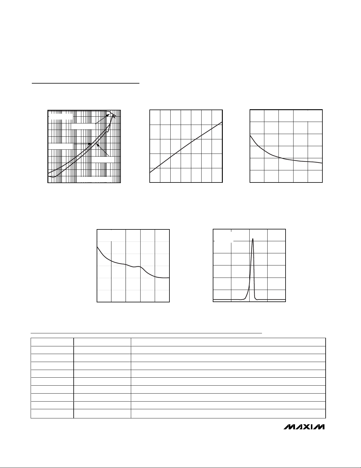
ON-RESISTANCE vs. V
COM
AND TEMPERATURE (SINGLE SUPPLY)
MAX4659/MAX4660 toc04
V
COM
(V)
R
ON
(Ω)
TA = +85°C
TA = +25°C
TA = -40°C
0.1
1
100
10
1000
10,000
-40 10-15 35 60 85
LEAKAGE CURRENT
vs. TEMPERATURE
MAX4659/MAX4660 toc05
TEMPERATURE (°C)
OFF-LEAKAGE (pA)
V+ = +15V
V- = -15V
I
COM(ON)
I
COM(OFF)
-60
-30
30
0
60
90
-15 -5-10 0 5 10 15
CHARGE INJECTION
vs. V
COM
MAX4659/MAX4660 toc06
V
COM
(V)
Q (pC)
A
B
A: V+ = 15V, V- = -15V
B: V+ = 12V, V- = 0
0
300
900
600
1200
1500
0101552025303540
SUPPLY CURRENT vs. SUPPLY VOLTAGE
(SINGLE SUPPLY)
MAX4659/MAX4660 toc07
SUPPLY VOLTAGE (V)
SUPPLY CURRENT (µA)
V- = 0
0
40
120
80
160
200
SUPPLY CURRENT vs. SUPPLY VOLTAGE
AND TEMPERATURE
MAX4659/MAX4660 toc08
SUPPLY VOLTAGE (V)
SUPPLY CURRENT (µA)
010515
A
B
C
D
F
DUAL SUPPLIES
V
COM
= 3V,
I
SWITCH
= 100mA,
IN = GND
A: I+, TA = -40°C
B: I+, T
A
= +25°C
C: I+, T
A
= +85°C
D: I-, T
A
= -40°C
E: I-, T
A
= +25°C
F: I-, T
A
= +85°C
E
0.0001
0.01
0.1
1
10 1k100 10k 100k
TOTAL HARMONIC DISTORTION
vs. FREQUENCY
MAX4659/MAX4660 toc09
FREQUENCY (Hz)
TOTAL HARMONIC DISTORTION (%)
V+ = 15V
V- = -15V
5V
RMS
SIGNAL
600Ω SOURCE AND
BW = 80kHz
0
10
5
25
20
15
30
35
50
45
40
55
081624 32 40
ON-RESISTANCE vs. V
COM
(SINGLE SUPPLY)
MAX4659/MAX4660 toc02
V
COM
(V)
R
ON
(Ω)
A
B
C
D
E
A: V+ = +9V, V- = 0
B: V+ = +12V, V- = 0
C: V+ = +24V, V- = 0
D: V+ = +36V, V- = 0
E: V+ = +40V, V- = 0
30
25
20
15
10
-15 0-10 -5 5 10 15
ON-RESISTANCE vs. V
COM
AND TEMPERATURE (DUAL SUPPLIES)
MAX4659/MAX4660 toc03
V
COM
(V)
R
ON
(Ω)
TA = +85°C
TA = +25°C
TA = -40°C
MAX4659/MAX4660
High-Current, 25ΩΩ, SPDT, CMOS
Analog Switches
_______________________________________________________________________________________ 5
0
10
5
20
15
50
30
25
35
40
45
55
-20 -10 0 10 20
ON-RESISTANCE vs. V
COM
(DUAL SUPPLIES)
MAX4659/MAX4660 toc01
V
COM
(V)
R
ON
(Ω)
D: V+ = +15V, V- = -15V
E: V+ = +20V, V- = -20V
A: V+ = +4.5V, V- = -4.5V
B: V+ = +10V, V- = -10V
C: V+ = +12V, V- = -12V
A
B
C
D
E
Typical Operating Characteristics
(TA = +25°C, unless otherwise noted.)
Page 6
Pin Description
PIN NAME FUNCTION
1 COM Analog Switch Common
2NCNormally Closed Switch Terminal. NC is connected to COM when IN is low.
3 GND Ground
4V+Positive Supply Voltage Input
5 N.C. No Connection
6INDigital Control Input
7V-Negative Supply Voltage Input
8NONormally Open Switch Terminal. NO is connected to COM when IN is high.
—EPExposed Paddle. Connect EP to V+ or leave unconnected.
MAX4659/MAX4660
High-Current, 25ΩΩ, SPDT, CMOS
Analog Switches
6 _______________________________________________________________________________________
Typical Operating Characteristics (continued)
(TA = +25°C, unless otherwise noted.)
0.01 0.1 1 10 100 1000
FREQUENCY RESPONSE
MAX4659/MAX4660 toc10
FREQUENCY (MHz)
LOSS (dB)
-110
-100
-90
-80
-70
-60
-50
-40
-30
-20
-10
0
ON-RESPONSE
OFF-ISOLATION
BW = 225MHz
CROSSTALK
V+ = 15V, V- = -15V
1.0
1.4
2.2
1.8
2.6
3.0
51510 20 25 30 35 40
LOGIC LEVEL THRESHOLD
VOLTAGE vs. SUPPLY VOLTAGE
MAX4659/MAX4660 toc11
V+ (V)
V
TH
(V)
0
100
50
200
150
250
300
597111315
TRANSISTION TIME
vs. SUPPLY VOLTAGE
MAX4659/MAX4660 toc12
V+, V- (V)
TRANSITION TIME (ns)
RL = 200Ω
C
L
= 35pF
0
20
10
40
30
50
60
597111315
BREAK-BEFORE-MAKE DELAY
vs. SUPPLY VOLTAGE
MAX4659/MAX4660 toc13
BREAK-BEFORE-MAKE DELAY (ns)
RL = 200Ω
C
L
= 35pF
0
1000
500
2000
1500
2500
3000
-10 0-5 5 10
SUPPLY CURRENT
vs. VOLTAGE ACROSS SWITCH
MAX4659/MAX4660 toc14
I + (µA)
V+ = +15V,
V- = -15V
Page 7

MAX4659/MAX4660
High-Current, 25ΩΩ, SPDT, CMOS
Analog Switches
_______________________________________________________________________________________ 7
Detailed Description
The MAX4659/MAX4660 are single, single-pole/doublethrow (SPDT) CMOS analog switches. The CMOS
switch construction provides rail-to-rail signal handling
while consuming very little power. The switch is controlled by a TTL/CMOS level compatible digital input.
The MAX4659/MAX4660 have a normally open switch
and a normally closed switch.
These devices can be operated with either single
power supplies or dual power supplies. Operation at up
to ±20V supplies allows users a wide switching dynamic range. Additionally, asymmetrical operation is possible to tailor performance to a particular application.
These switches have been specifically designed to
handle high switch currents, up to 200mA peak current
and 150mA continuous currents. In order to do this, a
new technique is used to drive the body of the output
N-channel device. (Note: The basic switch between the
input, NC/NO terminal and the output common terminal
consists of an N-channel MOSFET and a P-channel
MOSFET in parallel.) The standard method limits operation to approximately a 600mV drop across the switch.
More than 600mV causes an increase in IdONleakage
current (due to the turn-on of on-chip parasitic diodes),
and an increase in V+ supply current. With this new
sensing method, there is no limitation to the voltage
drop across the switch. Current and voltage are limited
only by the power dissipation rating of the package and
the absolute maximum ratings of the switch.
When the analog input voltage drop is approximately
7mV there is an increase in power supply current from
90µA to 2mA (typ) within a 1mV to 7mV range, caused
by the new sensing/driving circuitry.
Applications Information
Overvoltage Protection
Proper power-supply sequencing is recommended for
all CMOS devices. Do not exceed the absolute maximum ratings, because stresses beyond the listed ratings can cause permanent damage to the devices.
First, connect GND, followed by V+, V-, and the remaining pins. If power-supply sequencing is not possible,
add two small-signal diodes (D1, D2) in series with
supply pins (Figure 1). Adding diodes reduces the analog signal range to one diode drop below V+ and one
diode drop above V-, but does not affect the devices’
low switch resistance and low leakage characteristics.
Device operation is unchanged, and the difference
between V+ and V- should not exceed 44V. The protection diode for the negative supply is not required when
V- is connected to GND.
Off-Isolation at High Frequencies
In 50Ω systems, the high-frequency on-response of
these parts extends from DC to above 100MHz, with a
typical loss of -2dB. When the switch is turned off, however, it behaves like a capacitor and off-isolation
decreases with increasing frequency. This effect is
more pronounced with higher source and load impedances. Above 5MHz, circuit board layout becomes critical. The graphs shown in the Typical Operating
Characteristics were taken using a 50Ω source and
load connected with BNC connectors.
V+
COM
V-
N_
V
g
V+
D1
D2
V-
Figure 1. Overvoltage Protection Using Blocking Diodes
Page 8

50%
+3V
0
LOGIC
INPUT
SWITCH
OUTPUT
(V
OUT
)
0.9 ✕ V
OUT
t
BBM
LOGIC
INPUT
R
L
300Ω
GND
C
L
INCLUDES FIXTURE AND STRAY CAPACITANCE.
NO
IN
NC
V
OUT
V+
V+
C
L
35pF
+3V
COM
MAX4659/MAX4660
V-
V-
Figure 3. Break-Before-Make Time
Figure 4. Charge Injection
MAX4659/MAX4660
High-Current, 25ΩΩ, SPDT, CMOS
Analog Switches
8 _______________________________________________________________________________________
tR < 20ns
t
F
< 20ns
50%
0
V
NC
LOGIC
INPUT
V-
V-
R
L
300Ω
COM
GND
C
L
INCLUDES FIXTURE AND STRAY CAPACITANCE.
LOGIC
INPUT
NC
IN
t
TRANS
+3V
t
TRANS
V
O
V
NO
V+
NO
V
O
0.9V
NC
0.9V
NO
SWITCH
OUTPUT
MAX4659/MAX4660
V+
C
L
35pF
V
NC
V
NO
Figure 2. Functional Diagram
Test Circuits/Timing Diagrams
∆V
O
COM
GND
V
O
V
GEN
IN
OFF
IN DEPENDS ON SWITCH CONFIGURATION;
INPUT POLARITY DETERMINED BY SENSE OF SWITCH.
Q = (∆VO)(CL)
ON
OFF
V
IN
V+
V+
NC OR
V-
V-
= +3V
MAX4659/MAX4660
NO
V
O
C
L
1nF
Page 9

MAX4659/MAX4660
High-Current, 25ΩΩ, SPDT, CMOS
Analog Switches
_______________________________________________________________________________________ 9
IN
V
IN
SIGNAL
GENERATOR
V+
C
ANALYZER NC OR NO
R
L
GND
COM
C
V-
V-
MAX4659/MAX4660
V+
Figure 5. Off-Isolation
SIGNAL
GENERATOR
V+
C
ANALYZER
NO
R
L
GND
COM
C
V-
V-
IN
IN
NC
50Ω
MAX4659/MAX4660
V
V+
Figure 7. Channel Off-Capacitance
CAPACITANCE
METER
NC OR NO
COM
GND
C
V-
V-
IN
V
IN
C
V+
f = 1MHz
V+
MAX4659/MAX4660
Figure 8. Channel On-Capacitance
CAPACITANCE
METER
NC OR NO
COM
GND
C
V-
V-
IN
V
IN
C
V+
f = 1MHz
V+
MAX4659/MAX4660
Figure 6. Crosstalk
Test Circuits/Timing Diagrams (continued)
Chip Information
TRANSISTOR COUNT: 45
PROCESS: CMOS
Page 10
MAX4659/MAX4660
High-Current, 25ΩΩ, SPDT, CMOS
Analog Switches
10 ______________________________________________________________________________________
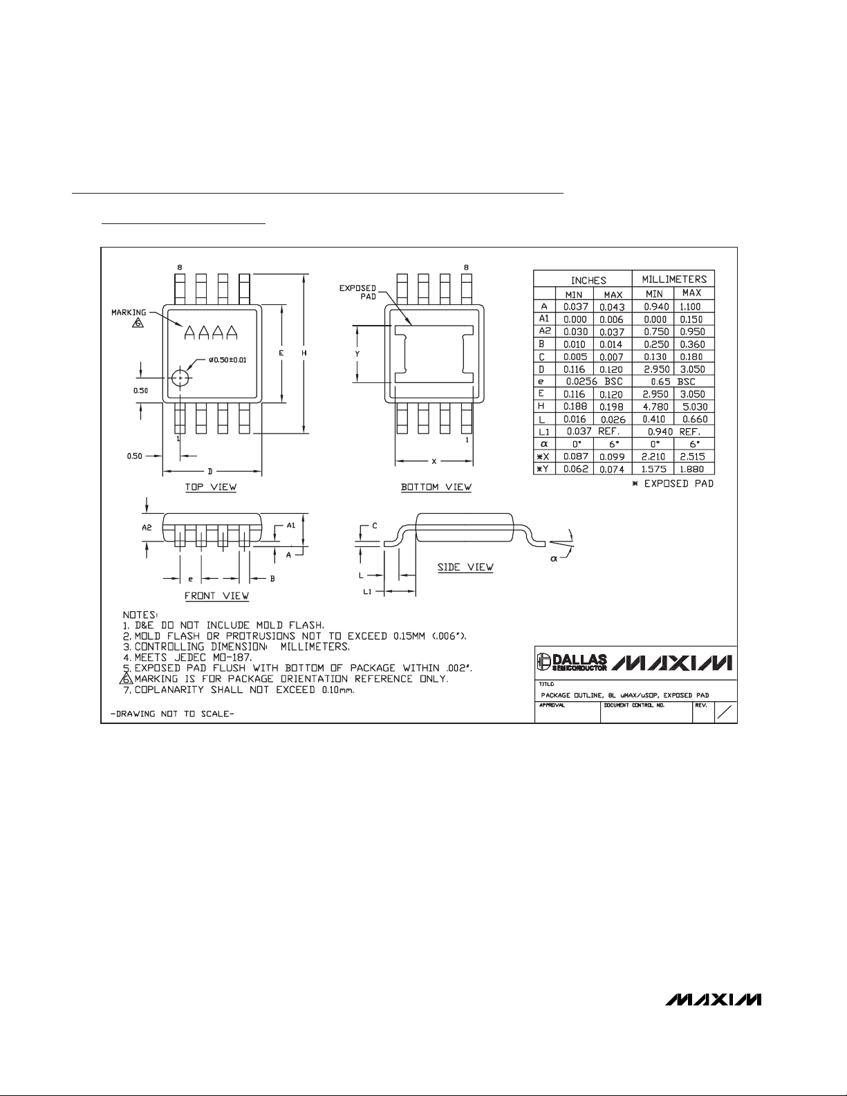
8L, µMAX, EXP PAD.EPS
C
1
1
21-0107
Package Information
(The package drawing(s) in this data sheet may not reflect the most current specifications. For the latest package outline information,
go to www.maxim-ic.com/packages
.)
Page 11

MAX4659/MAX4660
High-Current, 25ΩΩ, SPDT, CMOS
Analog Switches
______________________________________________________________________________________ 11
SOICN .EPS
PACKAGE OUTLINE, .150" SOIC
1
1
21-0041
B
REV.DOCUMENT CONTROL NO.APPROVAL
PROPRIETARY INFORMATION
TITLE:
TOP VIEW
FRONT VIEW
MAX
0.010
0.069
0.019
0.157
0.010
INCHES
0.150
0.007
E
C
DIM
0.014
0.004
B
A1
MIN
0.053A
0.19
3.80 4.00
0.25
MILLIMETERS
0.10
0.35
1.35
MIN
0.49
0.25
MAX
1.75
0.050
0.016L
0.40 1.27
0.3940.386D
D
MINDIM
D
INCHES
MAX
9.80 10.00
MILLIMETERS
MIN
MAX
16
AC
0.337 0.344 AB8.758.55 14
0.189 0.197 AA5.004.80 8
N MS012
N
SIDE VIEW
H 0.2440.228 5.80 6.20
e 0.050 BSC 1.27 BSC
C
HE
e
B
A1
A
D
0∞-8∞
L
1
VARIATIONS:
Package Information (continued)
(The package drawing(s) in this data sheet may not reflect the most current specifications. For the latest package outline information,
go to www.maxim-ic.com/packages
.)
Page 12
MAX4659/MAX4660
High-Current, 25ΩΩ, SPDT, CMOS
Analog Switches
Maxim cannot assume responsibility for use of any circuitry other than circuitry entirely embodied in a Maxim product. No circuit patent licenses are
implied. Maxim reserves the right to change the circuitry and specifications without notice at any time.
12 ____________________Maxim Integrated Products, 120 San Gabriel Drive, Sunnyvale, CA 94086 408-737-7600
© 2007 Maxim Integrated Products is a registered trademark of Maxim Integrated Products, Inc.
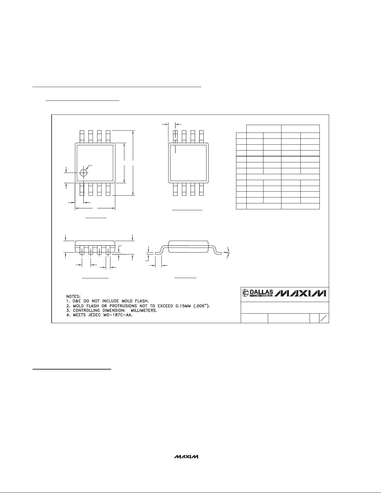
8LUMAXD.EPS
PACKAGE OUTLINE, 8L uMAX/uSOP
1
1
21-0036
J
REV.DOCUMENT CONTROL NO.APPROVAL
PROPRIETARY INFORMATION
TITLE:
MAX
0.043
0.006
0.014
0.120
0.120
0.198
0.026
0.007
0.037
0.0207 BSC
0.0256 BSC
A2
A1
c
e
b
A
L
FRONT VIEW
SIDE VIEW
E H
0.6±0.1
0.6±0.1
Ø0.50±0.1
1
TOP VIEW
D
8
A2
0.030
BOTTOM VIEW
1
6°
S
b
L
H
E
D
e
c
0°
0.010
0.116
0.116
0.188
0.016
0.005
8
4X S
INCHES
-
A1
A
MIN
0.002
0.950.75
0.5250 BSC
0.25 0.36
2.95 3.05
2.95 3.05
4.78
0.41
0.65 BSC
5.03
0.66
6°0°
0.13 0.18
MAX
MIN
MILLIMETERS
- 1.10
0.05 0.15
α
α
DIM
Package Information (continued)
(The package drawing(s) in this data sheet may not reflect the most current specifications. For the latest package outline information,
go to www.maxim-ic.com/packages
.)
Revision History
Pages changed at Rev 1: 1, 6, 12
 Loading...