

Page 1
General Description
Maxim’s MAX4655–MAX4658 are medium-voltage
CMOS analog switches with low on-resistance of 10Ω
max, specifically designed to handle large switch currents. With a switch capability of up to 400mA peak current and 300mA continuous current (MAX4655/
MAX4656), and up to 300mA peak current and 150mA
continuous current (MAX4657/MAX4658), these parts
can switch loads as low as 25Ω. They can replace reed
relays with a million times the speed and virtually unlimited number of lifetime cycles. Normal power consumption is only 3mW, whether the switch is on or off. These
parts are TTL/CMOS compatible and will switch any
voltage within its power-supply range.
These are SPST (single-pole/single-throw) switches.
The MAX4655/MAX4657 are normally closed (NC),
while the MAX4656/MAX4658 are normally open (NO).
The difference between the MAX4655/MAX4656 and
the MAX4657/MAX4658 is in the power dissipation of
their packages. Refer to the Absolute Maximum Ratings
and the Electrical Characteristics.
The MAX4655–MAX4658 power-supply range is from
±4.5V to ±20V for dual supply operation and +9V to
+40V for single supply operation. These switches can
operate from any combination of supplies, within a 40V
V+ to V- range. They conduct equally well in either direction and can handle Rail-to-Rail®analog signals. The offleakage current is only 1nA max at TA= +25°C. They are
available in 8-pin µMAX, QFN, and SO packages, with
exposed pad options for high-power applications.
Applications
Relay Replacement
Test Equipment
Communication Systems
xDSL Modems
PBX, PABX Systems
Audio Signal Routing
Audio Systems
PC Multimedia Boards
Redundant/Backup Systems
Features
♦ High Continuous Current Handling
300mA (MAX4655/MAX4656)
150mA (MAX4657/MAX4658)
♦ High Peak Current Handling
400mA (MAX4655/MAX4656)
300mA (MAX4657/MAX4658)
♦ 10Ω max On-Resistance (±15V supplies)
♦ VLnot Required
♦ 1Ω max RONFlatness over Specified Signal
Range
♦ Rail-to-Rail Signal Handling
♦ +12V Single Supply or ±15V Dual Supply
Operation
♦ Pin Compatible with DG417, DG418
MAX4655–MAX4658
High-Current, 10Ω, SPST, CMOS
Analog Switches
________________________________________________________________ Maxim Integrated Products 1
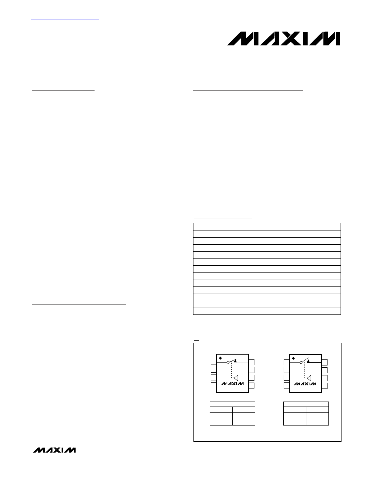
Ordering Information
TOP VIEW
1
2
4
8
7
6
5
NC
V-
IN
N.C.
V+
GND
N.C.
COM
µMAX/SO/QFN
SWITCHES SHOWN FOR LOGIC "0" INPUT
LOGIC SWITCH
0
1
ON
OFF
MAX4655/MAX4657
1
2
4
8
7
6
5
NO
V-
IN
N.C.
V+
GND
N.C.
COM
LOGIC SWITCH
0
1
OFF
ON
MAX4656/MAX4658
N.C. = NO CONNECT
NC = NORMALLY CLOSED
MAX4655/MAX4657
MAX4656/MAX4658
3
3
µMAX/SO/QFN
19-1984; Rev 1; 10/01
Rail-to-Rail is a registered trademark of Nippon Motorola, Ltd.
*EP = exposed pad
Pin Configurations/
Functional Diagrams/Truth Tables
For pricing, delivery, and ordering information, please contact Maxim/Dallas Direct! at
1-888-629-4642, or visit Maxim’s website at www.maxim-ic.com.
查询MAX4655供应商
PART TEMP. RANGE PIN-PACKAGE
MAX4655EGA -40°C to +85°C 8 QFN
MAX4655EUA -40°C to +85°C 8 µMAX-EP*
MAX4655ESA -40°C to +85°C 8 SO-EP*
MAX4656EGA -40°C to +85°C 8 QFN
MAX4656EUA -40°C to +85°C 8 µMAX-EP*
MAX4656ESA -40°C to +85°C 8 SO-EP*
MAX4657EGA -40°C to +85°C 8 QFN
MAX4657EUA -40°C to +85°C 8 µMAX
MAX4657ESA -40°C to +85°C 8 SO
MAX4658EGA -40°C to +85°C 8 QFN
MAX4658EUA -40°C to +85°C 8 µMAX
MAX4658ESA -40°C to +85°C 8 SO
Page 2
MAX4655–MAX4658
High-Current, 10Ω, SPST, CMOS
Analog Switches
2 _______________________________________________________________________________________
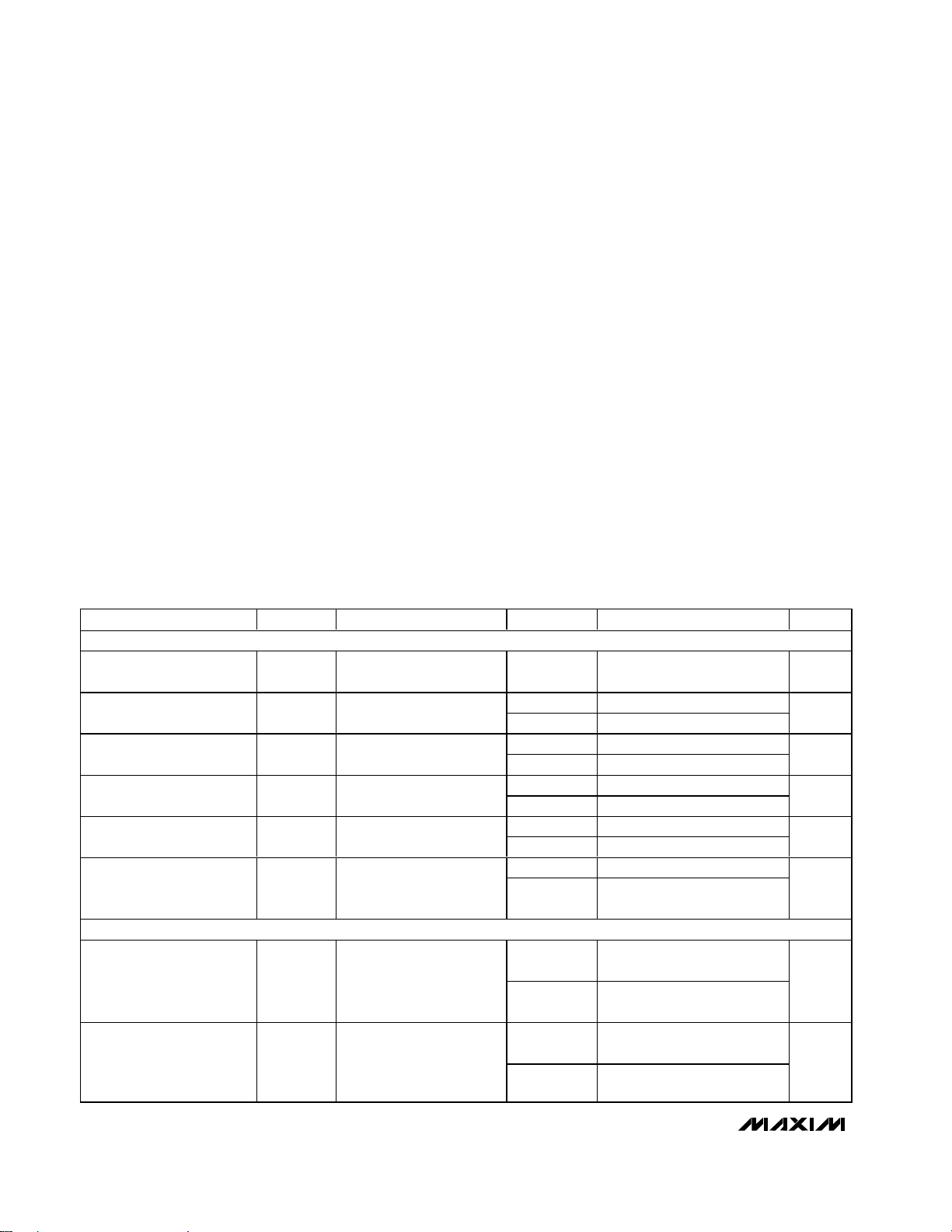
ABSOLUTE MAXIMUM RATINGS
ELECTRICAL CHARACTERISTICS—Dual Supplies
(V+ = +15V, V- = -15V, VIH= 2.4V, VIL= 0.8V, TA= T
MIN
to T
MAX
, unless otherwise noted. Typical values are at TA= +25°C.)
(Notes 2, 7)
Stresses beyond those listed under “Absolute Maximum Ratings” may cause permanent damage to the device. These are stress ratings only, and functional
operation of the device at these or any other conditions beyond those indicated in the operational sections of the specifications is not implied. Exposure to
absolute maximum rating conditions for extended periods may affect device reliability.
V+ to GND ..............................................................-0.3V to +44V
V- to GND ...............................................................-44V to +0.3V
V+ to V-...................................................................-0.3V to +44V
All Other Pins to GND (Note 1)..................V- - 0.3V to V+ + 0.3V
Continuous Current, COM, NO, NC
(MAX4655/MAX4656) ..................................................±300mA
Continuous Current, COM, NO, NC
(MAX4657/MAX4658) ..................................................±150mA
Continuous Current, IN .....................................................±30mA
Peak Current, COM, NO, NC
(pulsed at 1ms, 10% duty cycle)
MAX4655/MAX4656....................................................±400mA
(pulsed at 1ms, 10% duty cycle)
MAX4657/MAX4658....................................................±300mA
Continuous Power Dissipation (T
A
= +70°C)
8-Pin QFN (derate 24.4mW/°C above +70°C) ............195mW
8-Pin µMAX-EP (derate 10.3mW/°C above +70°C)
MAX4655/MAX4656 ....................................................825mW
8-Pin µMAX (derate 4.50mW/°C above +70°C)
MAX4657/MAX4658 ....................................................362mW
8-Pin SO-EP (derate 18.9mW/°C above +70°C)
MAX4655/MAX4656 ..................................................1509mW
8-Pin SO (derate 5.88mW/°C above +70°C)
MAX4657/MAX4658 ....................................................471mW
Operating Temperature Ranges
MAX4655–MAX4658..................................-40°C to +85°C
Junction Temperature......................................................+150°C
Storage Temperature Range .............................-65°C to +150°C
Lead Temperature (soldering, 10s) .................................+300°C
)
)
)
)
Note 1: Signals on NC, NO, COM, or IN exceeding V+ or V- will be clamped by internal diodes. Limit forward diode current to max-
imum current rating.
PARAMETER SYMBOL CONDITIONS T
ANALOG SWITCH
V
, VNC,
Analog Signal Range
On-Resistance R
On-Resistance Flatness
(Note 3)
NO or NC Off-Leakage
Current (Note 4)
COM Off-Leakage
Current (Note 4)
COM On-Leakage
Current (Note 4)
NO
V
COM
ON
R
FLAT (ON
I
NO(OFF)
I
NC(OFF
I
COM(OFF
I
COM(ON
I
= 100mA;
COM
or V
V
NO
I
= 100mA;
COM
or VNC = -5V, 0, +5V
V
NO
or
V
= +14.5V, -14.5V;
COM
or V
V
NO
V
COM
or VNC = -14.5V, +14.5V
V
NO
V
COM
V
or V
NO
-14.5V, or floating
NC
= +14.5V, -14.5V;
= +14.5V, -14.5V;
DYNAMIC CHARACTERISTICS
= ±10V
NC
= -14.5V, +14.5V
= +14.5V,
NC
A
MIN TYP MAX UNITS
V- V+ V
+25°C 7 10
T
to T
MIN
MAX
+25°C 0.3 1
T
to T
MIN
MAX
+25°C -1 0.01 1
T
MIN
to T
MAX
-10 10
+25°C -1 0.01 1
T
MIN
to T
MAX
-10 10
+25°C -2 2
T
MIN
to T
MAX
-20 20
15
1.5
Ω
Ω
nA
nA
nA
Turn-On Time t
Turn-Off Time t
ON
OFF
VNO or VNC = 10V;
R
= 50Ω; MAX4655/4656,
L
= 100Ω; MAX4657/4658,
R
L
C
= 35pF; Figure 3
L
VNO or VNC = 10V;
R
= 50Ω; MAX4655/4656,
L
= 100Ω; MAX4657/4658,
R
L
C
= 35pF; Figure 3
L
+25°C 110 200
to T
T
MIN
MAX
+25°C 75 100
to T
T
MIN
MAX
ns
300
ns
150
Page 3
MAX4655–MAX4658
High-Current, 10Ω, SPST, CMOS
Analog Switches
_______________________________________________________________________________________ 3
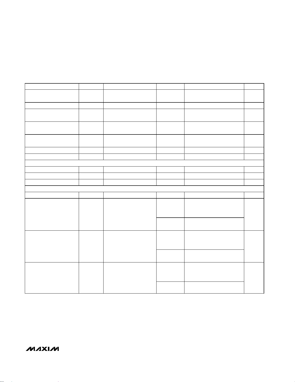
ELECTRICAL CHARACTERISTICS—Dual Supplies (continued)
(V+ = +15V, V- = -15V, VIH= 2.4V, VIL= 0.8V, TA= T
MIN
to T
MAX
, unless otherwise noted. Typical values are at TA= +25°C.)
(Notes 2, 7)
)
)
)
)
PARAMETER SYMBOL CONDITIONS T
V
= 0; R
GEN
Charge Injection Q
= 1nF; Figure 4
C
L
-3dB Bandwidth BW +25°C 210 MHz
Off-Isolation (Note 5) V
ISO
Total Harmonic Distortion THD
C
NO or NC Off-Capacitance
COM Off-Capacitance C
COM On-Capacitance C
NO(OFF
C
NC(OFF
COM(OFF
COM(ON
f = 1MHz; RL = 50Ω;
Figure 5
f = 20H z to 20kH z,
= 5V
V
N_
p-p
,
f = 1MHz; Figure 6 +25°C 25 pF
f = 1MHz; Figure 6 +25°C 25 pF
f = 1MHz; Figure 7 +25°C 67 pF
DIGITAL I/O
Input Logic High V
Input Logic Low V
Input Leakage Current I
IH
IL
IN
VIN = 0.8V or 2.4V T
POWER SUPPLY
Power-Supply Range T
= 0 or 5V, VN_ = 3V;
V
IN
= 200mA,
I
SWITCH
Positive Supply Current I+
MAX4655/4656;
I
= 100mA,
SWITCH
MAX4657/4658
GEN
= 0;
; RL = 600Ω
A
MIN TYP MAX UNITS
+25°C 23 pC
+25°C -77
+25°C 0.007 %
T
T
MIN
MIN
MIN
MIN
to T
to T
to T
to T
MAX
MAX
MAX
MAX
2.4 V
0.8 V
-1 1 µA
±4.5 ±20 V
+25°C 90 150
T
MIN
to T
MAX
300
dB
µA
Negative Supply Current I-
Ground Current I
GND
V
= 0 or 5V, VN_ = 3V;
IN
I
= 200mA,
SWITCH
MAX4655/4656;
I
= 100mA,
SWITCH
MAX4657/4658
VIN = 0 or 5V, VN_ = 3V;
SWITCH
= 200mA,
I
MAX4655/4656;
= 100mA,
I
SWITCH
MAX4657/4658
+25°C 10 50
to T
T
MIN
MAX
+25°C 80 130
to T
T
MIN
MAX
µA
100
µA
260
Page 4
MAX4655–MAX4658
High-Current, 10Ω, SPST, CMOS
Analog Switches
4 _______________________________________________________________________________________
)
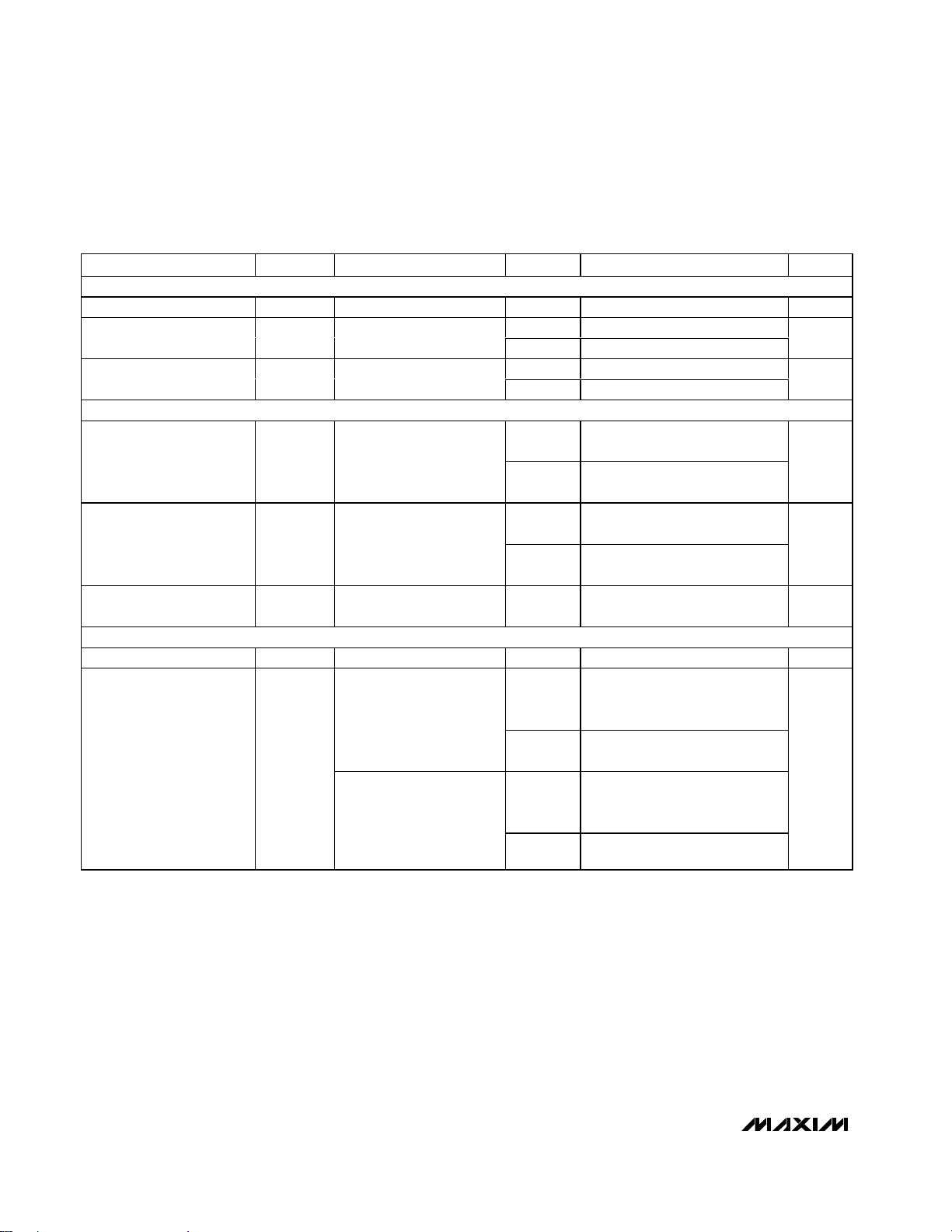
ELECTRICAL CHARACTERISTICS—Single Supply
(V+ = +12V, V- = 0, VIH= 2.4V, VIL= 0.8V, TA= T
MIN
to T
MAX
, unless otherwise noted. Typical values are at TA= +25°C.) (Note 2)
Note 2: The algebraic convention is used in this data sheet; the most negative value is shown in the minimum column.
Note 3: Flatness is defined as the difference between the maximum and minimum value of on-resistance as measured over the
specified analog signal range.
Note 4: Leakage parameters are 100% tested at maximum rated hot temperature and guaranteed by correlation at T
A
= +25°C.
Note 5: Off-isolation = 20log10[V
COM
/ (VNCor VNO)], V
COM
= output, VNCor VNO= input to off switch.
Note 6: Guaranteed by testing with dual supplies.
Note 7: -40°C specifications are quaranteed by design.
PARAMETER SYMBOL CONDITIONS T
ANALOG SWITCH
Analog Signal Range V
On-Resistance R
On-Resistance Flatness
(Note 3)
IN
ON
R
FLAT (ON
I
V
I
V
DYNAMIC CHARACTERISTICS
= 50mA,
COM
or VNC = 10V
NO
= 50mA,
COM
or V
N O
N C
T
MIN
to T
A
MAX
+25°C1522
T
to T
MIN
MAX
+25°C 2.2 4
= 2V , 6V , 10V
T
MIN
to T
MAX
MIN TYP MAX UNITS
0V+V
33
5
Ω
Ω
VNO or V
R
= 100Ω MAX4655/4656,
Turn-On Time t
ON
L
= 200Ω MAX4657/4658,
R
L
C
= 35pF; Figure 3
L
VNO or V
= 100Ω MAX4655/4656,
R
Turn-Off Time t
OFF
Charge Injection Q
L
R
= 200Ω MAX4657/4658,
L
= 35pF; Figure 3
C
L
V
GEN
= 1nF; Figure 4
C
L
NC
NC
= 0; R
= 10V;
= 10V;
GEN
= 0;
+25°C 140 200
T
MIN
to T
MAX
300
+25°C 65 125
T
MIN
to T
MAX
200
+25°C1 pC
POWER SUPPLY
Power-Supply Range V+ 9 40 V
VIN = 0 or 12V,
I
SWITCH
= 100mA,
+25°C 25 100
MAX4655/4656;
I
= 50mA,
Positive Supply Current
(Note 6)
SWITCH
MAX4657/4658
I+
= 0 or 5V,
V
IN
I
= 100mA,
SWITCH
T
to T
MIN
MAX
+25°C 46 125
200
MAX4655/4656;
I
= 50mA,
SWITCH
MAX4657/4658
T
MIN
to T
MAX
200
ns
ns
µA
Page 5

MAX4655–MAX4658
High-Current, 10Ω, SPST, CMOS
Analog Switches
_______________________________________________________________________________________ 5
Typical Operating Characteristics
(TA = +25°C, unless otherwise noted.)
ON-RESISTANCE vs. V
COM
(DUAL SUPPLIES)
25
20
15
(Ω)
ON
R
10
5
0
B
E
A: V+ = +4.5V, V- = -4.5V D: V+ = +15V, V- = -15V
B: V+ = +10V, V- = -10V E: V+ = +20V, V- = -20V
C: V+ = +12V, V- = -12V
-20 0-10 10 20
V
COM
ON-RESISTANCE vs. V
A
(V)
COM
AND TEMPERATURE (SINGLE SUPPLY)
25
20
(Ω)
15
ON
R
10
TA = +85°C
TA = +25°C
TA = -40°C
C
D
MAX4655/58 toc01
(Ω)
ON
R
10,000
MAX4655/58 toc04
OFF-LEAKAGE (pA)
ON-RESISTANCE vs. V
(SINGLE SUPPLY)
25
A
20
B
15
10
5
0
0168243240
C
E
V
COM
LEAKAGE CURRENT
vs. TEMPERATURE
V+ = +15V,
V- = -15V
1000
100
10
1
COM
A: V+ = +9V, V- = 0
B: V+ = +12V, V- = 0
C: V+ = +24V, V- = 0
D: V+ = +36V, V- = 0
E: V+ = +40V, V- = 0
D
(V)
I
COM(0N)
I
COM(0FF)
MAX4655/58 toc02
MAX4655/58 toc05
ON-RESISTANCE vs. V
AND TEMPERATURE (DUAL SUPPLIES)
15
10
(Ω)
ON
R
5
0
-15 -5 0-10 5 10 15
TA = +85°C
TA = +25°C
TA = -40°C
V
(V)
COM
CHARGE INJECTION
vs. V
COM
A
B
Q (pC)
-30
90
A: V+ = +15V, V- = -15V
B: V+ = +12V, V- = 0V
60
30
0
COM
MAX4655/58 toc03
MAX4655/58 toc06
5
0624 81012
V
(V)
COM
SUPPLY CURRENT vs. SUPPLY VOLTAGE
(SINGLE SUPPLY)
250
V- = 0
200
150
100
SUPPLY CURRENT (µA)
50
0
0 102030515253540
SUPPLY VOLTAGE (V)
0.1
60
50
MAX4655/58 toc07
40
30
20
SUPPLY CURRENT (µA)
10
0
-40 10-15 35 60 85
TEMPERATURE (°C)
SUPPLY CURRENT
vs. SUPPLY VOLTAGE AND TEMPERATURE
A: I+, TA = -40°C
= +25°C
B: I+, T
A
= +85°C
C: I+, T
A
= -40°C
D: I-, T
A
= +25°C
E: I-, T
A
= +85°C
F: I-, T
A
DUAL SUPPLIES:
= 3V,
±15V, V
COM
= 100mA
I
SWITCH
0 ±5 ±10 ±15
SUPPLY VOLTAGE (V)
A
B
C
D
E
F
-60
-15 -5-10 0 5 10 15
TOTAL HARMONIC DISTORTION
1
V+ = +15V
V- = -15V
5V
0.1
RMS
600Ω SOURCE
MAX4657/58 toc08
0.01
TOTAL HARMONIC DISTORTION (%)
0.001
V
vs. FREQUENCY
SIGNAL
FREQUENCY (Hz)
COM
(V)
MAX4655/58 toc09
1k100 10k 100k10
Page 6

MAX4655–MAX4658
High-Current, 10Ω, SPST, CMOS
Analog Switches
6 _______________________________________________________________________________________
Typical Operating Characteristics (continued)
(TA = +25°C, unless otherwise noted.)
-120
-80
-100
-40
-60
0
-20
20
0.01 10.1 10 100 1000
ON-RESPONSE, OFF-ISOLATION
vs. FREQUENCY
MAX4655/58 toc10
FREQUENCY (MHz)
LOSS (dB)
ON-RESPONSE
OFF-ISOLATION
BW = 210MHz
V+ = +15V,
V- = -15V
1.0
1.4
2.2
1.8
2.6
3.0
51510 20 25 30 35 40
LOGIC LEVEL THRESHOLD VOLTAGE
vs. SUPPLY VOLTAGE
MAX4655/58 toc11
V+ (V)
V
TH
(V)
0
1000
500
2000
1500
2500
3000
-10 0-5 5 10
SUPPLY CURRENT vs. VOLTAGE ACROSS
SWITCH
MAX4655/58 toc14
V
COM
- VN_ (mV)
I+ (µA)
V+ = +15V,
V- = -15V
0
40
120
80
160
200
-40 10-15 35 60 85
TURN-ON/TURN-OFF TIME
vs. TEMPERATURE
TEMPERATURE (°C)
t
ON
/t
OFF
(ns)
MAX4655/58 toc13
t
ON
t
OFF
V+ = +15V
V- = -15V
R
L
= 300Ω
C
L
= 35pF
Pin Description
TURN-ON/TURN-OFF TIME vs.
SUPPLY VOLTAGE (DUAL SUPPLIES)
300
250
200
(ns)
150
OFF
/t
ON
t
100
50
0
597111315
t
t
OFF
V+, V- (V)
RL = 300Ω
= 35pF
C
L
ON
MAX4655/58 toc12
PIN
MAX4655/
MAX4657
MAX4656/
MAX4658
1 1 COM Analog Switch Common
2, 5 2, 5 N.C. No Internal Connection
3 3 GND Ground
4 4 V+ Positive Supply Voltage Input
6 6 IN Digital Control Input
7 7 V- Negative Supply Voltage Input
— 8 NO Analog Switch Normally Open
8 — NC Analog Switch Normally Closed
NAME FUNCTION
Page 7

Detailed Description
The MAX4655–MAX4658 are single SPST CMOS analog switches. The CMOS switch construction provides
rail-to-rail signal handling while consuming very little
power. The switch is controlled by a TTL/CMOS level
compatible digital input. The MAX4655/MAX4657 are
normally closed switches, and the MAX4656/MAX4658
are normally open switches.
These devices can be operated with either single
power supplies or dual power supplies. Operation at up
to ±20V supplies allows users a wide switching dynamic
range. Additionally, asymmetrical operation is possible
to tailor performance to a particular application.
These switches have been specifically designed to
handle high switch currents, up to 400mA peak current
and 300mA continuous currents. In order to do this, a
new technique is used to drive the body of the output
N-channel device. (Note: the basic switch between the
input NC/NO terminal, and the output common terminal
consists of an N-channel MOSFET and a P-channel
MOSFET in parallel.) The standard method limits operation to approximately a 600mV drop across the switch.
More than 600mV causes an increase in IdONleakage
current (due to the turn-on of on-chip parasitic diodes)
and an increase in V+ supply current. With the new
sensing method, there is no limitation to the voltage
drop across the switch. Current and voltage are limited
only by the power dissipation rating of the package and
the absolute maximum ratings of the switch.
When the analog input to output voltage drop is
approximately 7mV there is an increase in power supply current from typically 90µA to 2mA within a 1mV to
7mV range, caused by the new sensing/driving circuitry.
Applications Information
Overvoltage Protection
Proper power-supply sequencing is recommended for
all CMOS devices. Do not exceed the absolute maximum ratings, because stresses beyond the listed ratings can cause permanent damage to the devices.
First, connect GND, followed by V+, V-, and the remaining pins. If power-supply sequencing is not possible,
add two small signal diodes (D1, D2) in series with supply pins (Figure 1). Adding diodes reduces the analog
signal range to one diode drop below V+ and one
diode drop above V-, but does not affect the devices’
low switch resistance and low leakage characteristics.
Device operation is unchanged, and the difference
between V+ and V- should not exceed 44V. The protection diode for the negative supply is not required when
V- is connected to GND.
Off-Isolation at High Frequencies
In 50Ω systems, the high-frequency on-response of
these parts extends from DC to above 100MHz, with a
typical loss of -2dB. When the switch is turned off, however, it behaves like a capacitor, and off-isolation
decreases with increasing frequency. This effect is
more pronounced with higher source and load impedances. Above 5MHz, circuit board layout becomes
critical. The graphs shown in the Typical Operating
Characteristics were taken using a 50Ω source and
load connected with BNC connectors.
MAX4655–MAX4658
High-Current, 10Ω, SPST, CMOS
Analog Switches
_______________________________________________________________________________________ 7
Figure 1. Overvoltage Protection Using Blocking Diodes
V+
V+
NO_
V
g
V-
V-
COM_
Page 8

MAX4655–MAX4658
High-Current, 10Ω, SPST, CMOS
Analog Switches
8 _______________________________________________________________________________________
Figure 3. Switching Time
Test Circuits/Timing Diagrams
Figure 2. Block Diagram
Figure 4. Charge Injection
NC
OR
NO
V+
COM
IN
GND
V-
+3V
LOGIC
INPUT
0
SWITCH
V
COM
INPUT
SWITCH
0
OUTPUT
50%
t
OFF
V
O
0.9V0 0.9V0
t
ON
LOGIC INPUT WAVEFORMS INVERTED FOR SWITCHES
THAT HAVE THE OPPOSITE LOGIC SENSE.
tR < 20ns
t
< 20ns
F
TTL/CMOS
LEVEL
SHIFTER
NO OR
LOGIC
INPUT
SENSOR
NC
SWITCH
INPUT
COM
IN
GND
INCLUDES FIXTURE AND STRAY CAPACITANCE.
C
L
V
= V
O
COM (
R
COM
RL
+15V
-15V
L + RON
V+
NC
OR NO
V-
)
MAX4655–
MAX4658
R
L
SWITCH
OUTPUT
C
L
35pF
V
O
∆V
O
V
O
IN
OFF
OFF
IN
IN DEPENDS ON SWITCH CONFIGURATION;
INPUT POLARITY DETERMINED BY SENSE OF SWITCH.
ON
ON
Q = (∆VO)(CL)
OFF
OFF
V
GEN
COM
GND
+15V
V+
NC OR
NO
V-
-15V
= +3V
V
IN
MAX4655–
MAX4658
C
L
1nF
V
O
Page 9

MAX4655–MAX4658
High-Current, 10Ω, SPST, CMOS
Analog Switches
_______________________________________________________________________________________ 9
Figure 6. Channel Off-Capacitance
Test Circuits/Timing Diagrams (continued)
Figure 5. Off-Isolation
Figure 7. Channel On-Capacitance
Chip Information
TRANSISTOR COUNT: 45
PROCESS: CMOS
SIGNAL
GENERATOR 0dBm
R
L
ANALYZER NC OR NO
C
C
COM
COM
+15V
V+
+15V
V+
GND
-15V
V-
MAX4655–
MAX4658
IN
MAX4655–
MAX4658
+15V
C
V+
COM
0V,
2.4V
C
CAPACITANCE
METER
f = 1MHz
NC OR NO
GND
-15V
MAX4655–
MAX4658
IN
V-
0V
C
CAPACITANCE
METER
f = 1MHz
NC OR NO
GND
V-
-15V
IN
2.4V
C
Page 10

MAX4655–MAX4658
High Current, 10Ω, SPST, CMOS
Analog Switches
10 ______________________________________________________________________________________
Package Information
6L, 8L QFN(DUAL).EPS
µ
Page 11

MAX4655–MAX4658
High Current, 10Ω, SPST, CMOS
Analog Switches
______________________________________________________________________________________ 11
Package Information (continued)
8LUMAXD.EPS
Page 12

MAX4655–MAX4658
High Current, 10Ω, SPST, CMOS
Analog Switches
Maxim cannot assume responsibility for use of any circuitry other than circuitry entirely embodied in a Maxim product. No circuit patent licenses are
implied. Maxim reserves the right to change the circuitry and specifications without notice at any time.
12 ____________________Maxim Integrated Products, 120 San Gabriel Drive, Sunnyvale, CA 94086 408-737-7600
© 2001 Maxim Integrated Products Printed USA is a registered trademark of Maxim Integrated Products.
Package Information (continued)
SOICN.EPS
 Loading...