

19-1906; Rev 0; 2/01
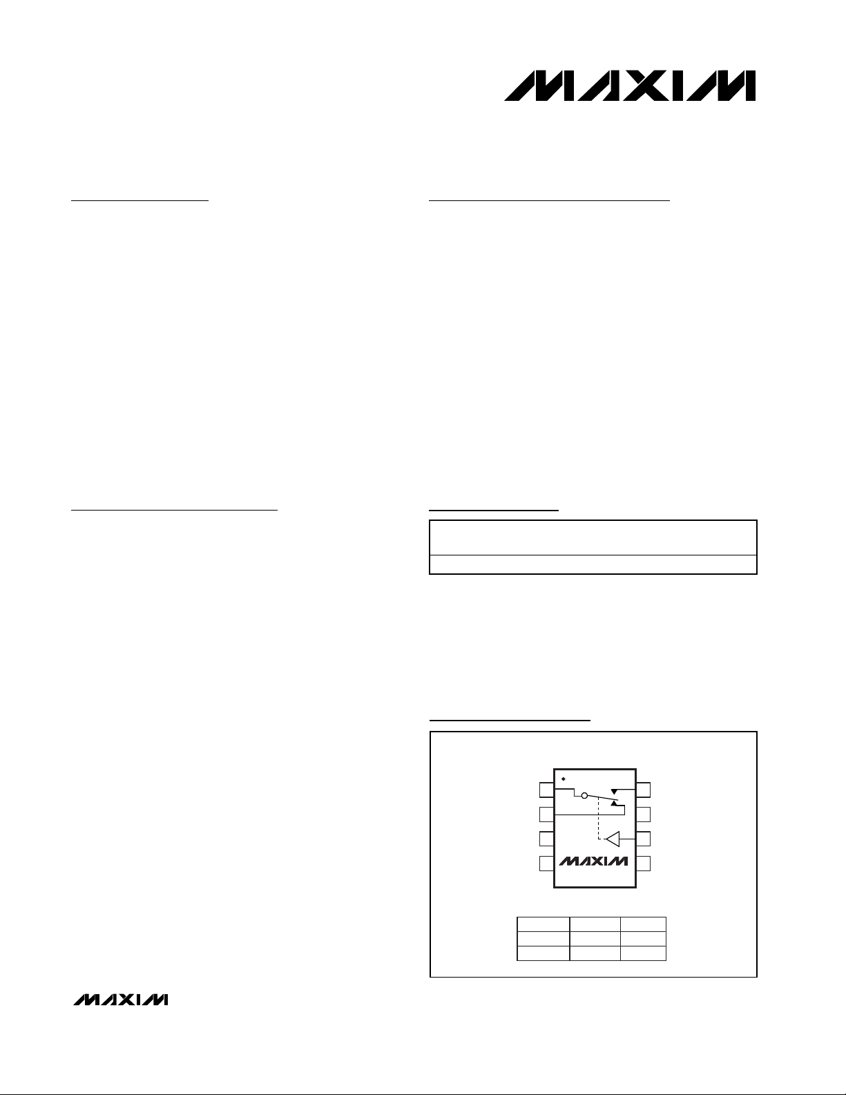
IN
N.C.V+
1
2
87NO
V-NC
GND
COM
SOT23-8
TOP VIEW
3
4
6
5
MAX4649
LOGIC
NO
0
1
OFF
ON
NC
ON
OFF
General Description
The MAX4649 is a dual-supply, single-pole/doublethrow (SPDT) analog switch. On-resistance is 45Ω max
and flat (7Ω max) over the specified signal range. The
MAX4649 can handle Rail-to-Rail®analog signals, and
conducts analog or digital signals equally well in either
direction. This switch operates from a single +9V to
+36V supply, or from ±4.5V to ±20V dual supplies. The
primary application areas are in the switching and routing of signals in telecommunications and test equipment.
The MAX4649 features a switch transition time of 130ns
max at +25°C, and a guaranteed break-before-make
switching time of 5ns. Off-leakage current is only 2nA
max at +25°C.
The MAX4649 is available in a tiny 8-pin SOT23 package.
Applications
PBX, PABX Systems
Communication Systems
DSL
Test Equipment
Avionics
Audio Systems
Redundant Systems
Relay Replacement
PC Multimedia Boards
Features
♦ Low On-Resistance 45Ω max ±15V Supplies
♦ 5Ω max R
ON
Match Between Channels
♦ Guaranteed R
ON
Flatness Over Specified Signal
Range (7Ω max)
♦ V
L
Logic Supply Not Required
♦ Rail-to-Rail Signal Handling
♦ +9V to +36V Single Supply Operation
♦ ±4.5V to ±20V Dual Supply Operation
♦ Low Crosstalk: -92dB at 1MHz
♦ High Off-Isolation: -92dB at 1MHz
♦ TTL/CMOS-Compatible Control Inputs
45Ω, SPDT Analog Switch in SOT23-8
MAX4649
________________________________________________________________ Maxim Integrated Products 1
For price, delivery, and to place orders, please contact Maxim Distribution at 1-888-629-4642,
or visit Maxim’s website at www.maxim-ic.com.
Pin Configuration
Ordering Information
Rail-to-Rail is a registered trademark of Nippon Motorola, Inc.
PART
MAX4649E KA- T- 40°C to + 85°C 8-SOT23 AAIE
TEMP.
RANGE
PINPA CK A G E
TOP
M ARK
MAX4649
45Ω, SPDT Analog Switch in SOT23-8
2 _______________________________________________________________________________________
ABSOLUTE MAXIMUM RATINGS
ELECTRICAL CHARACTERISTICS—Dual ±15V Supplies
(V+ = +15V, V- = -15V, VIH= 2.4V, VIL= 0.8V, TA= T
MIN
to T
MAX
, unless otherwise noted. Typical values are at TA= +25°C.) (Notes
2, 3)
Stresses beyond those listed under “Absolute Maximum Ratings” may cause permanent damage to the device. These are stress ratings only, and functional
operation of the device at these or any other conditions beyond those indicated in the operational sections of the specifications is not implied. Exposure to
absolute maximum rating conditions for extended periods may affect device reliability.
V+ ........................................................................-0.3V to +44.0V
V- .........................................................................-44.0V to +0.3V
V+ to V-................................................................-0.3V to +44.0V
All Other Pins (Note 1) ..........................(V- - 0.3V) to (V+ + 0.3V)
Continuous Current into any Terminal ..............................±10mA
Continuous Current (COM, NO, NC) ................................±30mA
Peak Current (COM, NO, NC)
(pulsed at 1ms, 10% duty cycle)..................................±60mA
Continuous Power Dissipation (T
A
= +70°C)
8-Pin SOT23 (derate 8.9mW/°C above +70°C)...........714mW
Operating Temperature Range
MAX4649EKA ............................................-40°C to +85°C
Storage Temperature Range .............................-65°C to +150°C
Junction Temperature......................................................+150°C
Lead Temperature (soldering, 10s) .................................+300°C
Note 1: Signals on NO, NC, COM, or IN exceeding V+ or V- are clamped by internal diodes. Limit forward-diode current to maxi-
mum current rating.
)
)
(Voltages referenced to GND.)
PARAMETER SYMBOL CONDITIONS T
ANALOG SWITCH
,
V
NO
,
Analog Signal Range
On-Resistance R
On-Resistance Matching Between
Channels
On-Resistance Flatness
(Note 4)
NO or NC Off-Leakage
Current
V
NC
V
COM
ON
∆R
ON
R
FLAT
(ON)
I
NO(OFF)
or
I
NC(OFF
I
V
I
V
I
V
V
V
-14V
= 1mA; V
COM
= ±10V
NC
= 1mA; VNO or
COM
= ±10V
NC
= 1mA; V
COM
= +5V, 0, -5V
NC
= -14V, +14V;
COM
or VNC = +14V,
NO
A
NO
or
+25°C3345
T
to T
MIN
MAX
+25°C 0.6 5
T
to T
MIN
MAX
NO
or
+25°C 1.5 7
T
to T
MIN
MAX
+25°C -2 0.01 2
T
to T
MIN
MAX
MIN TYP MAX UNITS
V- V+ V
60
6
10
-10 10
Ω
Ω
Ω
nA
COM On-Leakage
Current
I
COM(ON
V
= +14V, -14V;
COM
or VNC = +14V,
V
NO
-14V or floating
+25°C-4 4
T
MIN
to T
MAX
-20 20
DIGITAL I/O
Input Logic High Voltage V
Input Logic Low Voltage V
Input Leakage I
IH
IL
IN
VIN = 0 or +5V -1 1 µA
2.4 V
nA
0.8 V
MAX4649
45Ω, SPDT Analog Switch in SOT23-8
_______________________________________________________________________________________ 3
)
)
ELECTRICAL CHARACTERISTICS—Dual ±15V Supplies (continued)
(V+ = +15V, V- = -15V, VIH= 2.4V, VIL= 0.8V, TA= T
MIN
to T
MAX
, unless otherwise noted. Typical values are at TA= +25°C.) (Notes
2, 3)
PARAMETER SYMBOL CONDITIONS T
DYNAMIC CHARACTERISTICS
VNO or V
Transition Time t
TRANS
R
C
VNO or V
Break-Before-Make Delay t
R
D
C
V
Charge Injection Q
C
Figure 4
f = 1MHz, RL = 50Ω,
Off-Isolation V
ISO
C
V
Figure 5
Crosstalk
Total Harmonic Distortion THD
C
V
or V
NC
Off-Capacitance
NO
COM On-Capacitance C
NO(OFF)
C
NC(OFF
COM(ON
f = 1MHz, R
C
f = 20Hz to 20kHz,
R
,
f = 1MHz; Figure 7 6 pF
f = 1MHz; Figure 8 17 pF
POWER SUPPLY
Power-Supply Range ±4.5 ±20 V
VIN = 5V
Positive Supply Current I+
V
Negative Supply Current I- VIN = 0 or 5V
= ±10V;
NC
NC
= 0; R
= 1V
= ±10V;
GEN
;
RMS
= 50Ω,
L
RMS
= 1kΩ;
L
= 35pF; Figure 2
L
= 300Ω;
L
= 35pF; Figure 3
L
GEN
= 1nF;
L
= 5pF,
L
COM
= 5pF; Figure 6
L
= 600Ω, 5V
L
= 0 or V+
IN
A
MIN TYP MAX UNITS
+25°C 90 130
T
MIN
to T
MAX
170
+25°C510
T
MIN
to T
MAX
2
= 0;
2pC
92 dB
92
0.015 %
+25°C3875
T
MIN
to T
MAX
100
+25°C 0.01 1
T
MIN
to T
MAX
10
+25°C 0.01 1
T
MIN
to T
MAX
10
ns
ns
µA
µA

MAX4649
45Ω, SPDT Analog Switch in SOT23-8
4 _______________________________________________________________________________________
ELECTRICAL CHARACTERISTICS—Single +12V Supply
(V+ = +12V, V- = 0, VIH= 2.4V, VIL= 0.8V, TA= T
MIN
to T
MAX
, unless otherwise noted. Typical values are at TA= +25°C.) (Notes 2, 3)
Note 2: The algebraic convention is used in this data sheet; the most negative value is shown in the minimum column.
Note 3: All parts are 100% tested at +25°C. Limits across the full temperature range are guaranteed by design and correlation.
Note 4: Flatness is defined as the difference between the maximum and minimum value of on-resistance as measured over the
specified analog signal range.
PARAMETER SYMBOL CONDITIONS T
ANALOG SWITCH
Analog Signal Range
On-Resistance R
On-Resistance Matching Between
Channels
On-Resistance Flatness
(Note 4)
R
FL AT ( ON )
DYNAMIC
Transition Time t
V
NO
V
NC
V
COM
ON
∆R
ON
TRANS
,
,
I
COM
= 1mA; V
or VNC = +10V
I
= 1mA; V
COM
or VNC = +10V
I
= 1mA; V
COM
or V
= +2V, +6V,
NC
+10V
VNO or V
NC
= 0,
10V or 10V, 0;
R
= 1kΩ;
L
C
= 35pF;
L
Figure 2
NO
NO
NO
A
+25°C6890
T
to T
MIN
MAX
+25°C 0.7 6
T
to T
MIN
MAX
+25°C917
T
to T
MIN
MAX
+25°C 116 165
to T
T
MIN
MAX
MIN TYP MAX UNITS
0V+V
115
7
Ω
Ω
Ω
23
ns
200
Break-Before-Make Delay t
Charge Injection Q
VNO or V
+10V; R
D
= 35pF;
C
L
Figure 3
V
GE N
= 1nF; Figure 4
C
L
NC
= 300Ω;
L
= 0; R
=
GE N
= 0;
+25°C136
ns
T
MIN
to T
MAX
1
+25°C1pC
POWER SUPPLY
Power Supply Range 936V
+25°C2240
to T
T
MIN
MAX
+25°C 0.01 1
T
to T
MIN
MAX
50
10
µA
Positive Supply Current I+
VIN = +5V
V
= 0 or V+
IN

30
50
40
70
60
90
80
100
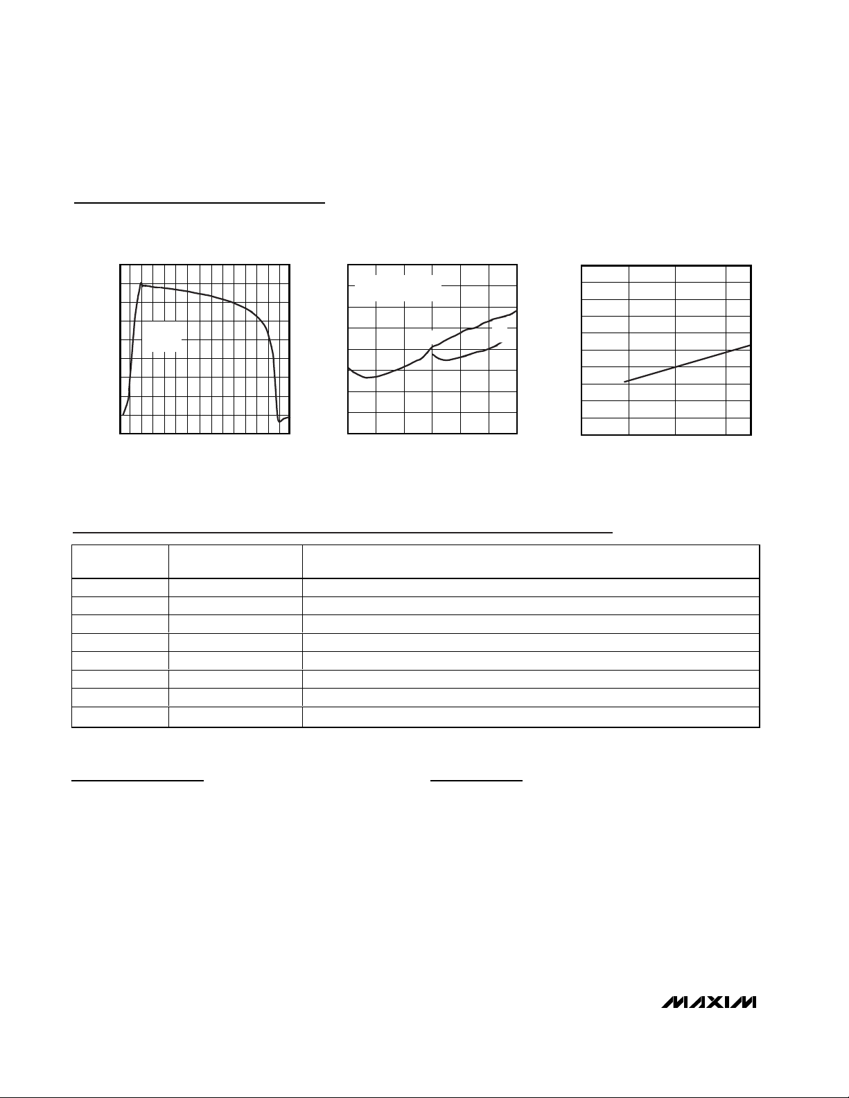
0 5 10 15
MAX4649 toc04
V
COM
(V)
R
ON
(Ω)
ON-RESISTANCE vs. V
COM
AND TEMPERATURE
V+ = +12V
V- = 0
TA = +85°C
TA = -40°C
TA = +25°C
0.00001
0.001
0.0001
0.1
0.01
1
10
-40 0 20-20 40 60 80
ON-LEAKAGE CURRENT
vs. TEMPERATURE
MAX4649 toc05
TEMPERATURE (°C)
ON-LEAKAGE (nA)
V+ = +15V
V- = -15V
V
COM
= ±10V
DUAL SUPPLIES
0.001
0.0001
0.1
0.01
1
-40 0 20-20 406080
OFF-LEAKAGE CURRENT
vs. TEMPERATURE
MAX4649 toc06
TEMPERATURE (°C)
DUAL SUPPLIES
V+ = +15V
V- = -15V
V
COM
= 10V
OFF-LEAKAGE (nA)
VNC OR VNO = ±10V
±
0
-100
0.1 100101 1000
FREQUENCY RESPONSE
MAX4649 toc07
FREQUENCY (MHz)
LOSS (dB)
-90
-80
-70
-60
-50
-40
-30
-20
-10
-110
ON-RESPONSE
OFF-ISOLATION
CROSSTALK
100
0.0001
10 1k 10k100 100k
TOTAL HARMONIC DISTORTION
vs. FREQUENCY
MAX4649 toc08
FREQUENCY (Hz)
DISTORTION (%)
0.001
0.01
0.1
1
10
SIGNAL DISTORTION
V+ = +15V
V- = -15V
600Ω SOURCE
AND LOAD
MEASUREMENT LIMITS
5V
RMS
SIGNAL
10
30
20
60
50
40
90
80
70
100
-40 10-15 356085
SUPPLY CURRENT
vs. TEMPERATURE
MAX4649 toc09
I+ (µA)
TEMPERATURE (°C)
V+ = +15V
V- = -15V
IN = 5V
I+
20
30
40
50
60
70
80
90
100
0 10203040
MAX4649 toc02
V
COM
(V)
R
ON
(Ω)
V+ = +9V
V+ = +12V
V+ = +18V
V+ = +36V
V+ = +30V
V+ = +24V
ON-RESISTANCE vs. V
COM
(SINGLE SUPPLY)
10
15
20
25
30
35
40
45
50
-15 -5-10 0 5 10 15
ON-RESISTANCE vs. V
COM
AND TEMPERATURE
MAX4649 toc03
V
COM
(V)
R
ON
(Ω)
V+ = +15V
V- = -15V
TA = +85°C
TA = -40°C
TA = +25°C
MAX4649
45Ω, SPDT Analog Switch in SOT23-8
_______________________________________________________________________________________ 5
Typical Operating Characteristics
(TA = +25°C, unless otherwise noted.)
ON-RESISTANCE vs. V
COM
(DUAL SUPPLIES)
90
A: V+ = +8V, V- = -8V
B: V+ = +10V, V- = -10V
80
C: V+ = +12V, V- = -12V
D: V+ = +15V, V- = -15V
70
E: V+ = +20V, V- = -20V
60
(Ω)
ON
R
50
40
30
20
-20 -10 0 10 20
V
COM
A
B
C
D
(V)
MAX4649 toc01
E
Pin Description
PIN NAME FUNCTION
1 COM Analog Switch Common
2 NC Normally Closed Switch Terminal. NC is connected to COM when IN is low.
3 GND Ground
4 V+ Positive Supply Voltage Input
5 N.C. No Connection
6 IN Digital Control Input
7 V- Negative Supply Voltage Input
8 NO Normally Open Switch Terminal. NO is connected to COM when IN is high.
MAX4649
Detailed Description
The MAX4649 is a high-voltage, single-pole/doublethrow (SPDT) analog switch that operates from dual
±4.5V to ±20V supplies or from a single +9V to +36V
supply. The MAX4649 has one normally closed (NC)
switch and one normally open (NO) switch. CMOS
switch construction allows bidirectional processing of
rail-to-rail analog signals.
The MAX4649 has break-before-make switching. The
transition time for switching from one input to the other
is typically 90ns. The off-leakage is typically less than
10pA, and on-leakage is typically less than 20pA.
Applications Information
Overvoltage Protection
Proper power-supply sequencing is recommended for
all CMOS devices. Do not exceed the absolute maximum ratings, because stresses beyond the listed ratings can cause permanent damage to the devices.
Always sequence V+ on first, then V-, followed by the
logic inputs, NO_, or COM. If power-supply sequencing is not possible, add two small signal diodes (D1,
D2) in series with supply pins (Figure 1). Adding
diodes reduces the analog signal range to one diode
drop below V+ and one diode drop above V-, but does
not affect the device’s low switch resistance and low
45Ω, SPDT Analog Switch in SOT23-8
6 _______________________________________________________________________________________
Typical Operating Characteristics (continued)
(TA = +25°C, unless otherwise noted.)
0.000001
0.0001
0.00001
0.1
0.01
0.001
1
10
100
1000
0231 456 78910111213
SUPPLY CURRENT
vs. LOGIC VOLTAGE
MAX4649 toc10
IN (V)
I+ (µA)
14 15
V+ = +15V
V- = -15V
-40
-30
-20
-10
0
10
20
30
40
-15 -5-10 0 5 10 15
CHARGE INJECTION
vs. V
COM
MAX4649 toc11
V
COM
(V)
CHARGE (pC)
A: V+ = +15V, V- = -15V
B: V+ = +12V, V- = 0
A
B
0
1.5
1.0
0.5
2.0
2.5
3.0
3.5
4.0
4.5
5.0
01020 30
LOGIC THRESHOLD
vs. SUPPLY VOLTAGE
MAX4649 toc12
V+ (V)
LOGIC THRESHOLD (V)

MAX4649
45Ω, SPDT Analog Switch in SOT23-8
_______________________________________________________________________________________ 7
leakage characteristics. Device operation is unchanged, and the difference between V+ and V- should
not exceed 44V. These protection diodes are not recommended when using a single supply.
Off-Isolation at High Frequencies
In 50Ω systems, the high-frequency on-response of
these parts extends from DC to above 300MHz, with a
typical loss of -3.6dB. When the switch is turned off,
however, it behaves like a capacitor, and off-isolation
decreases with increasing frequency. This effect is
more pronounced with higher source and load impedances. Above 5MHz, circuit board layout becomes critical. The graphs shown in the Typical Operating
Characteristics were taken using a 50Ω source and
load connected with BNC connectors.
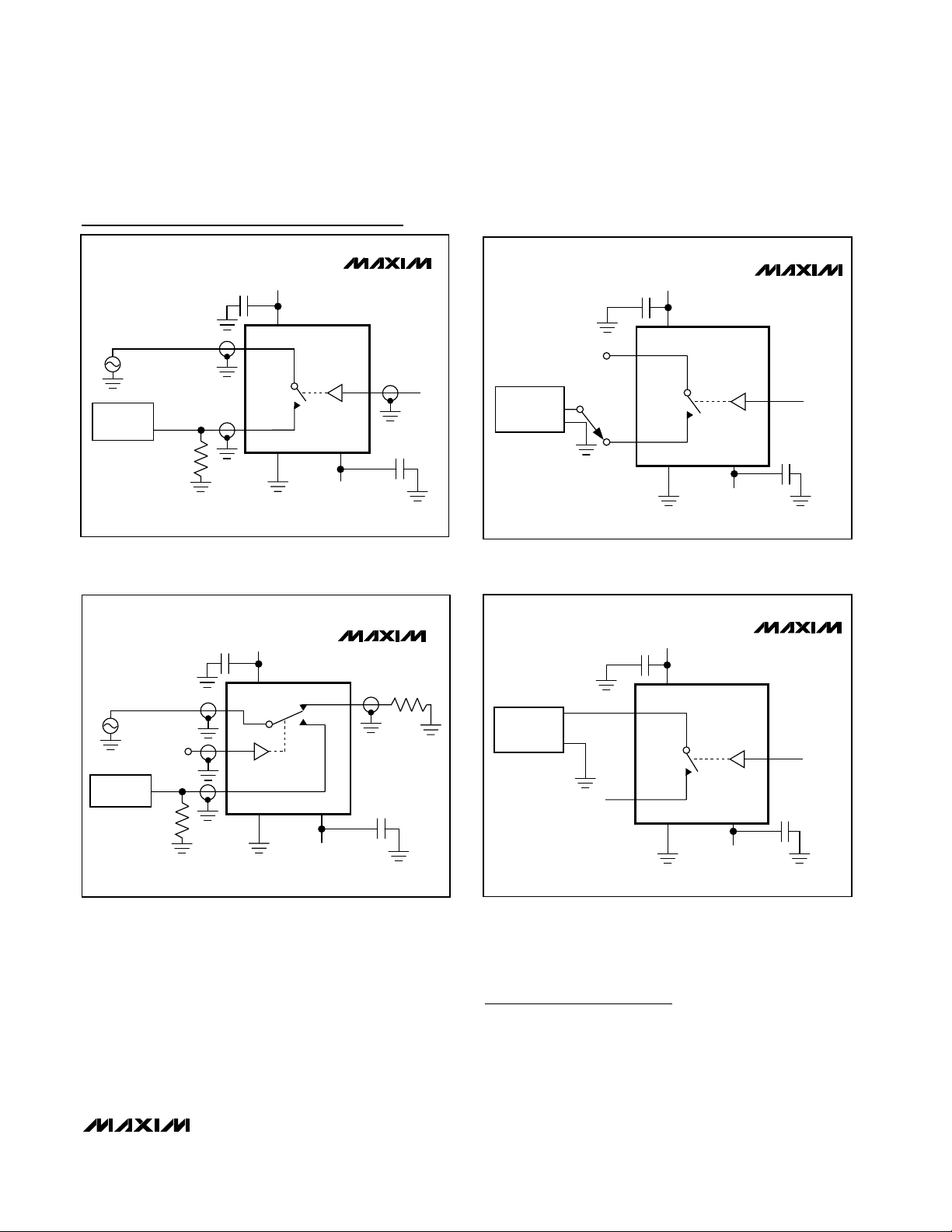
Figure 2. MAX4649 Transition Time
Test Circuits/Timing Diagrams
Figure 1. Overvoltage Protection
NO_
V
g
V+
D1
V+
COM
V-
D2
V-
+3V
LOGIC
INPUT
SWITCH
OUTPUT
0
V
NO
V
O
V
NC
50%
t
TRANS
0.9V
tR < 20ns
t
< 20ns
F
t
TRANS
0.9V
NO
NC
LOGIC
INPUT
V
NC
V
NO
C
+V
V+
NC
COM
NO
IN
GND
INCLUDES FIXTURE AND STRAY CAPACITANCE.
L
V-
-V
R
L
1000Ω
V
O
C
L
35pF
MAX4649

MAX4649
45Ω, SPDT Analog Switch in SOT23-8
8 _______________________________________________________________________________________
Figure 3. MAX4649 Break-Before-Make Test Circuit
Figure 4. Charge Injection
Test Circuits/Timing Diagrams (continued)
MAX4649
+3V
NC
NO
V+
V+
COM
IN
LOGIC
INPUT
C
L
V
O
IN
OFF
GND
INCLUDES FIXTURE AND STRAY CAPACITANCE.
ON
Q = (∆VO)(CL)
IN DEPENDS ON SWITCH CONFIGURATION;
INPUT POLARITY DETERMINED BY SENSE OF SWITCH.
R
300Ω
∆V
+3V
LOGIC
INPUT
OUT
COM
0
)
GND
V
OUT
L
C
L
35pF
SWITCH
OUTPUT
(V
O
V
GEN
OFF
50%
0.9 ✕ V
OUT
t
D
V+
V+
NC OR
NO
V-
V-
= +3V
V
IN
MAX4649
V
O
C
L
10nF
MAX4649
45Ω, SPDT Analog Switch in SOT23-8
_______________________________________________________________________________________ 9
Figure 5. Off-Isolation
Figure 7. Channel-Off Capacitance
Figure 8. COM On-Capacitance
Figure 6. Crosstalk Between Switches
Test Circuits/Timing Diagrams (continued)
Chip Information
TRANSISTOR COUNT: 33
PROCESS TECHNOLOGY: CMOS
C
SIGNAL
GENERATOR
ANALYZER NC OR NO
R
L
C
COM
V+
V+
GND
V-
V-
MAX4649
IN
MAX4649
V+
C
V+
COM
V
IN
CAPACITANCE
METER
C
f = 1MHz
NC OR NO
GND
V-
V+
C
MAX4649
IN
V-
V
IN
C
MAX4649
SIGNAL
GENERATOR
ANALYZER
V
IN
R
L
COM
IN
NO
GND
NC
V-
V-
50Ω
CAPACITANCE
METER
f = 1MHz
C
V+
COM
NC OR NO
GND
IN
V-
V-
V
IN
C
MAX4649
45Ω, SPDT Analog Switch in SOT23-8
Maxim cannot assume responsibility for use of any circuitry other than circuitry entirely embodied in a Maxim product. No circuit patent licenses are
implied. Maxim reserves the right to change the circuitry and specifications without notice at any time.
10 ____________________Maxim Integrated Products, 120 San Gabriel Drive, Sunnyvale, CA 94086 408-737-7600
© 2001 Maxim Integrated Products Printed USA is a registered trademark of Maxim Integrated Products.
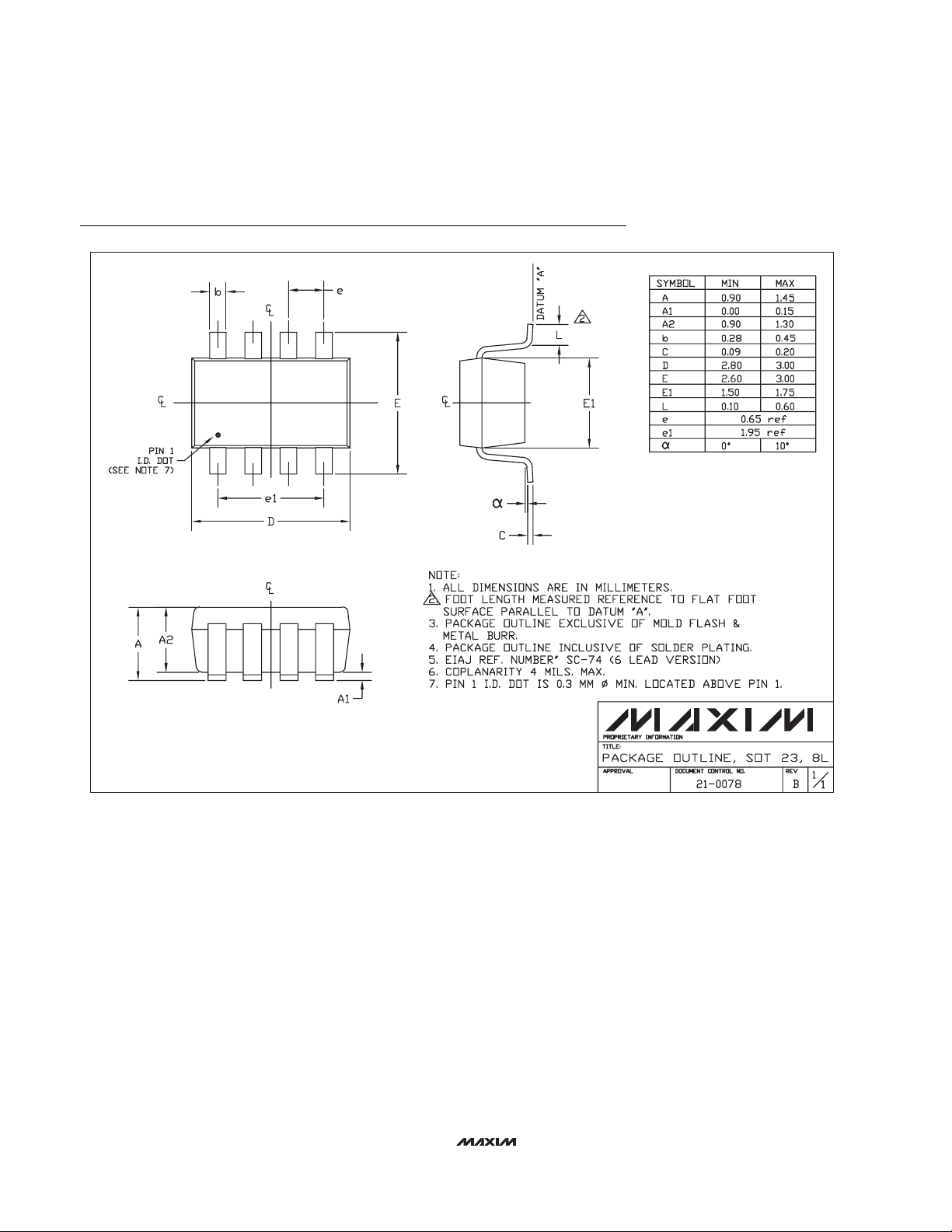
Package Information
SOT23, 8L.EPS
 Loading...