

Page 1
General Description
The MAX4647/MAX4648 are dual-supply single-pole/single-throw (SPST) switches. On-resistance is 25Ω max and
flat (2Ω max) over the specified signal range. Each switch
can handle rail-to-rail analog signals. Off-leakage current
is only 1nA max at +25°C. They conduct analog or digital
signals equally well in either direction. The primary application areas are in the switching and routing of signals in
telecommunications and test equipment.
The MAX4647/MAX4648 are single SPST analog switches.
The MAX4647 has one normally closed (NC) switch, and
the MAX4648 has one normally open (NO) switch. These
devices operate from a single +9V to +36V supply or from
dual ±4.5V to ±20V supplies. The MAX4647/MAX4648 are
available in tiny 6-pin SOT23 packages.
________________________Applications
PBX, PABX Systems
Communication Systems
DSL
Test Equipment
Avionics
Audio Systems
Redundant Systems
Relay Replacement
PC Multimedia Boards
____________________________Features
♦ Low On-Resistance 25Ω max (±15V Supplies)
♦ Guaranteed R
ON
Flatness Over Specified Signal
Range (2Ω max)
♦ V
L
Logic Supply Not Required
♦ Rail-to-Rail Signal Handling
♦ ±15V and Single 12V Supply Operation
♦ Low Leakage (1nA max)
♦ Fast Switching Speeds
t
ON
= 100ns
t
OFF
= 100ns
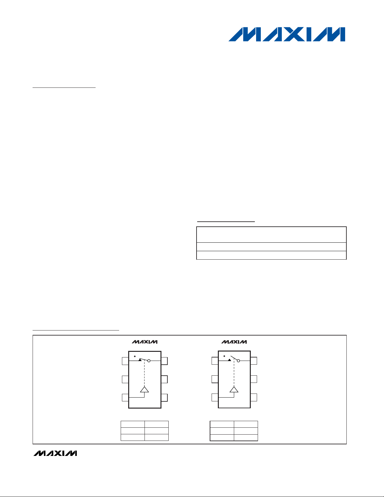
MAX4647/MAX4648
25Ω SPST Analog Switches in SOT23-6
________________________________________________________________ Maxim Integrated Products 1
V-
GNDIN
16COM
5 V+
NC
MAX4647
SOT23-6
TOP VIEW
2
34
LOGIC
SWITCH
0
1
ON
OFF
LOGIC
SWITCH
0
1
OFF
ON
V-
GNDIN
16COM
5 V+
NO
MAX4648
SOT23-6
2
34
Pin Configurations/Functional Diagrams/Truth Tables
19-1880; Rev 1; 1/07
For price, delivery, and to place orders, please contact Maxim Distribution at 1-888-629-4642,
or visit Maxim’s website at www.maxim-ic.com.
PART
TEMP
RANGE
PIN-
TOP
PKG
CODE
MAX4647EUT-T+
U 6S N - 1
MAX4648EUT-T+
U 6S N - 1
Ordering Information
+Denotes a lead-free package.
PACKAGE
-40°C to +85°C 6 SOT23 AARV
-40°C to +85°C 6 SOT23 AARW
MARK
Page 2
MAX4647/MAX4648
25Ω SPST Analog Switches in SOT23-6
2 _______________________________________________________________________________________
ABSOLUTE MAXIMUM RATINGS
ELECTRICAL CHARACTERISTICS—Dual ±15V Supplies
(V+ = +15V, V- = -15V, VIH= 2.4V, VIL= 0.8V, TA= T
MIN
to T
MAX
, unless otherwise noted. Typical values are at TA= +25°C.)
(Notes 2, 3)
Stresses beyond those listed under “Absolute Maximum Ratings” may cause permanent damage to the device. These are stress ratings only, and functional
operation of the device at these or any other conditions beyond those indicated in the operational sections of the specifications is not implied. Exposure to
absolute maximum rating conditions for extended periods may affect device reliability.
(Voltages referenced to GND)
V+ ...........................................................................-0.3V, +44.0V
V- ............................................................................-44.0V, +0.3V
V+ to V-................................................................-0.3V to +44.0V
All Other Pins (Note 1)...............................V- - 0.3V to V+ + 0.3V
Continuous Current into Any Terminal..............................±60mA
Peak Current into Any Terminal
(pulsed at 1ms, 10% duty cycle)...............................±100mA
Continuous Power Dissipation (T
A
= +70°C)
6-Pin SOT23 (derate 8.7mW/°C above +70°C)...........696mW
Operating Temperature Ranges
MAX464_EUT..................................................-40°C to +85°C
Storage Temperature Range .............................-65°C to +150°C
Junction Temperature......................................................+150°C
Lead Temperature (soldering, 10s) .................................+300°C
PARAMETER
SYMBOL
CONDITIONS T
A
MIN
TYP
MAX
UNITS
ANALOG SWITCH
Analog Signal Range
V
COM
V- V+ V
+25°C1825
On-Resistance R
ON
I
COM
= 10mA; V
NO
or V
NC
= ±10V
T
MIN
to T
MAX
30
Ω
+25°C 0.8 2
On-Resistance
Flatness (Note 4)
)
I
COM
= 10mA; V
NO
or V
NC
= +5V, 0, -5V
T
MIN
to T
MAX
3
Ω
+25°C-1
1
NO or NC Off-Leakage
Current
)
V
NO
or V
NC
= +14V, -14V;
V
COM
= -14V, +14V
T
MIN
to T
MAX
10
nA
+25°C-1
1
COM Off-Leakage
Current
)
V
COM
= -14V, +14V;
V
NO
or V
NC
= +14V, -14V
T
MIN
to T
MAX
10
nA
+25°C-2 2
COM On-Leakage
Current
)
V
COM
= +14V, -14V;
V
NO
or V
NC
= +14V, -14V or
floating
T
MIN
to T
MAX
20
nA
LOGIC INPUT
Input Logic High V
IH
T
MIN
to T
MAX
V
Input Logic Low V
IL
T
MIN
to T
MAX
0.8 V
Input Leakage Current
I
IN
V
IN
= 0 or +5V T
MIN
to T
MAX
-1 1 µA
DYNAMIC CHARACTERISTICS
+25°C68
Turn-On Time t
ON
VNO or V
NC
= ±10V; RL = 300Ω;
C
L
= 35pF; Figure 2
T
MIN
to T
MAX
ns
+25°C62
Turn-Off Time t
OFF
VNO or V
NC
= ±10V; R
L
=300Ω;
C
L
= 35pF; Figure 2
T
MIN
to T
MAX
ns
Charge Injection Q
COM
= 0; RS = 0; CL = 1nF;
Figure 3
+25°C4pC
Note 1: Signals on NO, NC, COM, or IN exceeding V+ or V- are clamped by internal diodes. Limit forward-diode current to
maximum current rating.
VNO,VNC,
R
FLAT(ON
I
NO(OFF)
I
NC(OFF
I
COM(OFF
I
COM(ON
or
0.01
-10
0.01
-10
-20
2.4
100
125
100
125
Page 3
MAX4647/MAX4648
25Ω SPST Analog Switches in SOT23-6
________________________________________________________________________________________ 3
MAX4647/MAX4648
PARAMETER
CONDITIONS T
A
TYP
UNITS
Off-Isolation V
ISO
CL = 5pF; RL = 50Ω; f = 1MHz;
V
COM
= 1V
RMS
; Figure 4
+25°C -92 dB
Total Harmonic
Distortion
THD
RL = 600Ω, 5Vp-p,
f = 20Hz to 20kHz
+25°C
%
V
NO
or V
NC
Off-Capacitance
C
NO(OFF)
,
)
f = 1MHz; Figure 5 +25°C6pF
COM Off-Capacitance
)
f = 1MHz; Figure 5 +25°C6pF
COM On-Capacitance
)
f = 1MHz; Figure 6 +25°C19pF
POWER SUPPLY
Power Supply Range T
MIN
to T
MAX
V
+25°C45
VIN = 5V
T
MIN
to T
MAX
+25°C
1
Positive Supply Current
I+
V
IN
= 0 or V+
T
MIN
to T
MAX
10
µA
+25°C
1
Negative Supply
Current
I- V
IN
= 0 or 5V
T
MIN
to T
MAX
10
µA
ELECTRICAL CHARACTERISTICS—Dual ±15V Supplies (continued)
(V+ = +15V, V- = -15V, VIH= 2.4V, VIL= 0.8V, TA= T
MIN
to T
MAX
, unless otherwise noted. Typical values are at TA= +25°C.
(Notes 2, 3)
ELECTRICAL CHARACTERISTICS—Single +12V Supply
(V+ = +12V, V- = 0, V
IH
= 2.4V, VIL= 0.8V, TA= T
MIN
to T
MAX
, unless otherwise noted. Typical values are at TA= +25°C.)
(Notes 2, 3)
PARAMETER
SYMBOL
CONDITIONS T
A
MIN
TYP
MAX
UNITS
ANALOG SWITCH
Analog Signal Range
VNO, VNC,
V
COM
0V+V
+25°C3645
On-Resistance R
ON
I
COM
= 10mA; V
NO
or VNC = +10V
T
MIN
to T
MAX
60
Ω
+25°C46
On-Resistance
Flatness (Note 4)
)
I
COM
= 10mA; V
NO
or V
NC
= +2V, +6V, +10V
T
MIN
to T
MAX
8
Ω
DYNAMIC
+25°C
Turn-On Time t
ON
V
N O
or V
N C
= + 10V ; RL = 300Ω;
C
L
= 35p F; Fi g ur e 2
T
MIN
to T
MAX
ns
+25°C68
Turn-Off Time t
OFF
V
N O
or V
N C
= + 10V ; RL = 300Ω;
C
L
= 35p F; Fi g ur e 2
T
MIN
to T
MAX
ns
Charge Injection Q
COM
= 0; RS = 0; CL = 1nF;
Figure 3
+25°C-5pC
SYMBOL
C
NC(OFF
C
COM(OFF
C
COM(ON
MIN
MAX
0.006
±4.5 ±20
100
150
0.001
0.001
R
FLAT(ON
100 175
225
150
200
Page 4

MAX4647/MAX4648
25Ω SPST Analog Switches in SOT23-6
4 _______________________________________________________________________________________
Typical Operating Characteristics
(TA = +25°C, unless otherwise noted.)
10
15
20
25
30
35
40
45
50
-20 -10 0 10 20
ON-RESISTANCE
vs. V
COM
(DUAL SUPPLIES)
MAX4647/48 toc01
V
COM
(V)
R
ON
(Ω)
A: V+ = +8, V- = -8V
B: V+ = +10V, V- = -10V
C: V+ = +12V, V- = -12V
D: V+ = +15V, V- = -15V
E: V+ = +20V, V- = -20V
A
B
C
D
E
10
15
20
25
30
35
40
45
50
0102030
ON-RESISTANCE
vs. V
COM
(SINGLE SUPPLY)
MAX4647/48 toc02
V
COM
(V)
R
ON
(Ω)
V+ = +12V
V+ = +9V
V+ = +24V
V+ = +36V
0
10
5
20
15
25
30
-15 -5 0-10 5 10 15
ON-RESISTANCE vs.
V
COM
AND TEMPERATURE (DUAL SUPPLIES)
MAX4647/48 toc03
V
COM
(V)
R
ON
(Ω)
TA = +85°C
TA = +25°C
TA = -40°C
V+ = +15V
V- = -15V
15
20
25
30
35
40
45
50
55
0 5 10 15
ON-RESISTANCE vs.
V
COM
AND TEMPERATURE (SINGLE SUPPLY)
MAX4647/48 toc04
V
COM
(V)
R
ON
(Ω)
TA = +85°C
TA = +25°C
TA = -40°C
V+ = +12V
V- = O
0.00001
0.001
0.0001
0.1
0.01
1
10
-40 20 40-20 0 60 80
ON-LEAKAGE CURRENT
vs. TEMPERATURE
MAX4647/48 toc05
TEMPERATURE (°C)
ON-LEAKAGE (nA)
V+ = +15V
V- = -15V
V
COM
= 10V
DUAL SUPPLIES
SINGLE SUPPLY
±
0.0001
0.001
0.01
0.1
1
OFF-LEAKAGE CURRENT
vs. TEMPERATURE
MAX4647/48 toc06
TEMEPERATURE (°C)
OFF-LEAKAGE (nA)
-40 20 40-20 0 60 80
V+ = +15V
V- = -15V
V
NC
OR V
NO =
±10V
V
COM
= 10V
DUAL SUPPLIES
SINGLE SUPPLY
±
ELECTRICAL CHARACTERISTICS—Single +12V Supply (continued)
(V+ = +12V, V- = 0, V
IH
= 2.4V, VIL= 0.8V, TA= T
MIN
to T
MAX
, unless otherwise noted. Typical values are at TA= +25°C.)
(Notes 2, 3)
PARAMETER
SYMBOL
CONDITIONS T
A
MIN
TYP
MAX
UNITS
Power Supply Range
T
MIN
to T
MAX
+9
V
+25°C2050
VIN = 5V
T
MIN
to T
MAX
75
+25°C
1
Positive Supply
Current
I+
V
IN
= 0 or V+
T
MIN
to T
MAX
10
µA
Note 2: The algebraic convention is used in this data sheet; the most negative value is shown in the minimum column.
Note 3: SOT packaged parts are 100% tested at +25°C. Limits across the full temperature range are guaranteed by design and
correlation.
Note 4: Flatness is defined as the difference between the maximum and minimum value of on-resistance as measured over the
specified analog signal range.
+36
0.001
Page 5

MAX4647/MAX4648
25Ω SPST Analog Switches in SOT23-6
_______________________________________________________________________________________ 5
Typical Operating Characteristics (continued)
(TA = +25°C, unless otherwise noted.)
Pin Description
02314
SUPPLY CURRENT
vs. LOGIC THRESHOLD
MAX4647/48 toc10
IN (V)
I+ (µA)
5786 9 10 12 1311 14
15
0.000001
0.0001
0.00001
0.1
0.01
0.001
1
10
100
1000
V+ = +15V
V- = -15V
V
COM
= +14V
-40
-30
-20
-10
0
10
20
30
40
-15 -5-10 0 5 10 15
CHARGE INJECTION vs. V
COM
MAX4647/48 toc11
V
COM
(V)
CHARGE (pC)
A: V+ = +15V, V- = -15V
B: V+ = +12V, V- = 0
A
B
0
1.5
1.0
0.5
2.0
2.5
3.0
3.5
4.0
4.5
5.0
0 102030
LOGIC THRESHOLD
vs. SUPPLY VOLTAGE
MAX4647/48 toc12
V+ (V)
LOGIC THRESHOLD (V)
MAX4647
MAX4648
PIN NAME
FUNCTION
1 — NC Normally Closed Switch Terminal
— 1 NO Normally Open Switch Terminal
2 2 V- Negative Supply Voltage Input
3 3 IN Digital Control Input
4 4 GND Ground
5 5 V+ Positive Supply Voltage Input
6 6 COM Analog Switch Common
FREQUENCY RESPONSE
0
-10
ON-RESPONSE
-20
-30
-40
-50
LOSS (dB)
-60
-70
-80
-90
-100
OFF-ISOLATION
0.1 1 10 100 1000
FREQUENCY (MHz)
TOTAL HARMONIC DISTORTION
MAX4647/48 toc07
DISTORTION (%)
0.01
0.001
0.0001
vs.FREQUENCY
100
V+ = +15V
V- = -15V
10
1
0.1
SIGNAL
5V
RMS
600Ω SOURCE
AND LOAD
SIGNAL DISTORTION
MEASUREMENT LIMITS
10 1k 10k100 100k
FREQUENCY (Hz)
MAX4647/48 toc08
SUPPLY CURRENT vs. TEMPERATURE
100
V+ = +15V
V- = -15V
10
IN = 5V
1
(µA)
GND
0.1
I+, I-, I
0.01
0.001
-40 10-15 35 60 85
TEMPERATURE (°C)
I+, I
GND
I-
MAX4647/48 toc09
Page 6

Applications Information
Overvoltage Protection
Proper power-supply sequencing is recommended for
all CMOS devices. Do not exceed the absolute maximum ratings because stresses beyond the listed ratings can cause permanent damage to the devices.
Always sequence V+ on first, then V-, followed by the
logic inputs, NO, NC, or COM. If power-supply
sequencing is not possible, add two small signal
diodes (D1, D2) in series with supply pins (Figure 1).
Adding diodes reduces the analog signal range to one
diode drop below V+ and one diode drop above V-, but
does not affect the devices’ low switch resistance and
low leakage characteristics. Device operation is
unchanged, and the difference between V+ and Vshould not exceed 44V. These protection diodes are
not recommended when using a single supply.
Off-Isolation at High Frequencies
In 50Ω systems, the high-frequency on-response of
these parts extends from DC to above 300MHz, with a
typical loss of -2dB. When the switch is turned off, however, it behaves like a capacitor, and off-isolation
decreases with increasing frequency. This effect is
more pronounced with higher source and load impedances. Above 5MHz, circuit board layout becomes critical. The graphs shown in the Typical Operating
Characteristics were taken using a 50Ω source and
load connected with BNC connectors.
MAX4647/MAX4648
25Ω SPST Analog Switches in SOT23-6
6 _______________________________________________________________________________________
tr < 20ns
tf < 20ns
50%
0
LOGIC
INPUT
V-
V-
R
L
300Ω
NO
OR NC
GND
CL INCLUDES FIXTURE AND STRAY CAPACITANCE.
V
O
= V
COM (
RL
)
RL + RON
SWITCH
INPUT
IN
+3V
t
OFF
0
COM
SWITCH
OUTPUT
0.9V
0
0.9V
0
t
ON
V
O
SWITCH
OUTPUT
LOGIC
INPUT
LOGIC INPUT WAVEFORMS INVERTED FOR SWITCHES
THAT HAVE THE OPPOSITE LOGIC SENSE.
V+
C
L
35pF
V+
V
O
V
COM
0
REPEAT TEST FOR EACH SWITCH. FOR LOAD
CONDITIONS, SEE Electrical Characteristics.
MAX4647
MAX4648
Figure 2. Switching-Time Test Circuit
V+
COM
D2
D1
V-
NO
V
g
V+
V-
MAX4647
MAX4648
Figure 1. Overvoltage Protection Using External Blocking
Diodes
Page 7

MAX4647/MAX4648
25Ω SPST Analog Switches in SOT23-6
________________________________________________________________________________________ 7
IN 0 OR 3V
SIGNAL
GENERATOR
V+
C
ANALYZER
NC OR NO
R
L
GND
COM
C
V-
V-
V+
MAX4647
MAX4648
Figure 4. Off-Isolation Test Circuit
CAPACITANCE
METER
NC OR NO
COM
GND
C
V-
V-
IN
0 OR 3V
C
V+
f = 1MHz
V+
MAX4647
MAX4648
Figure 5. Channel-Off Capacitance Test Circuit
V
GEN
GND
NC OR
NO
C
L
V
O
V-
V-
V+
V
O
V
IN
OFF
ON
OFF
∆V
O
Q = (∆VO)(CL)
COM
VIN DEPENDS ON SWITCH CONFIGURATION;
INPUT POLARITY DETERMINED BY SENSE OF SWITCH.
OFF
ON
OFF
V
IN
VIN = +3V
V+
R
GEN
IN
MAX4647
MAX4648
Figure 3. Charge Injection Test Circuit
Page 8

MAX4647/MAX4648
25Ω SPST Analog Switches in SOT23-6
8 _______________________________________________________________________________________
CAPACITANCE
METER
NC OR NO
COM
GND
C
V-
-15V
IN
0 OR 3V
C
+15V
f = 1MHz
V+
MAX4647
MAX4648
Figure 6. Channel-On Capacitance Test Circuit
Chip Information
TRANSISTOR COUNT: 24
PROCESS TECHNOLOGY: CMOS
Page 9

MAX4647/MAX4648
25Ω SPST Analog Switches in SOT23-6
Maxim cannot assume responsibility for use of any circuitry other than circuitry entirely embodied in a Maxim product. No circuit patent licenses are
implied. Maxim reserves the right to change the circuitry and specifications without notice at any time.
Maxim Integrated Products, 120 San Gabriel Drive, Sunnyvale, CA 94086 408-737-7600 _____________________ 9
© 2007 Maxim Integrated Products is a registered trademark of Maxim Integrated Products, Inc.
Package Information
(The package drawing(s) in this data sheet may not reflect the most current specifications. For the latest package outline information,
go to www.maxim-ic.com/packages
.)
Revision History
Pages changed at Rev 1: 1, 9
6LSOT.EPS
 Loading...