

Page 1
General Description
The MAX4645/MAX4646 single-pole, single-throw (SPST)
analog switches feature a 2.5Ω typical on-resistance
(RON) from a +5V supply. RONis flat (0.4Ω max) over the
specified signal range. Each switch can handle Rail-toRail®analog signals. Off-leakage current is 0.25nA max at
+25°C. These analog switches are ideal in low-distortion
applications and are the preferred solution over mechanical relays in automated test equipment or applications
where current switching is required. They have low power
requirements, require less board space, and are more
reliable than mechanical relays.
These switches operate from a +1.8V to +5V single supply, making them ideal for use in battery-powered applications. The MAX4645/MAX4646 have fast switching speeds
of 12ns turn-on time (tON) and 8ns turn-off time (t
OFF
).
The MAX4645 is a normally open (NO) switch, and the
MAX4646 is a normally closed (NC) switch. Both are
available in 5-pin SOT23, 6-pin SOT23, and 8-pin µMAX
packages.
________________________Applications
Battery-Powered Systems
Audio and Video Signal Routing
Low-Voltage Data-Acquisition Systems
Sample-and-Hold Circuits
Communications Circuits
Relay Replacement
____________________________Features
♦ +1.8V to +5V Single-Supply Operation
♦ Guaranteed R
ON
2.5Ω max (5V supply)
3.5Ω max (3V supply)
♦ 1.8V Operation
R
ON
30Ω typ Over Temperature
t
ON
40ns typ, t
OFF
20ns typ
♦ Low R
ON
Flatness: 0.4Ω max
♦ Guaranteed Low Leakage Currents
±0.25nA at +25°C
♦ Rail-to-Rail Output Capability
♦ TTL/CMOS-Logic Compatible
♦ -75dB Off-Isolation at 1MHz
♦ Low Distortion: 0.014% typ
MAX4645/MAX4646
Fast, Low-Voltage, 2.5Ω, SPST,
CMOS Analog Switches
________________________________________________________________ Maxim Integrated Products 1
19-1653; Rev 2; 2/04
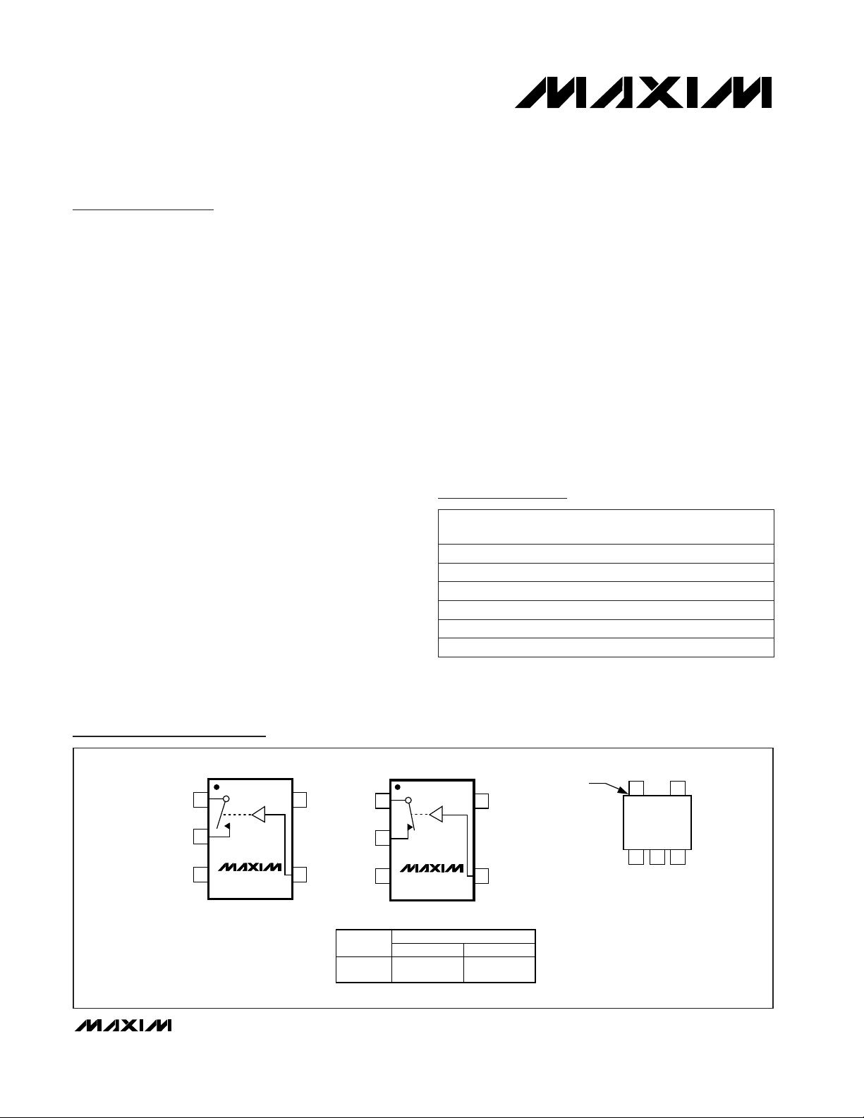
Ordering Information
Pin Configurations/Functional Diagrams/Truth Tables
µMAX/SO/DIP
PIN 5
5
XYZA
4
123
NOTE: SOT23-5 PACKAGE
HAS LETTERING NEAREST PIN 5.
TOP VIEW
IN
GND
1
5
V+
COM
MAX4645
2
3
4
SOT23-5
INPUT
0
1
SWITCH STATE
MAX4645
OFF
ON
MAX4646
ON
OFF
SWITCHES SHOWN FOR LOGIC 0 INPUT.
NO
µMAX/SO/DIP
IN
GND
1
5
V+
COM
MAX4646
2
3
4
SOT23-5
NC
MAX4645EUT-T -40°C to +85°C
PART TEMP RANGE
MAX4645EUK-T
-40°C to +85°C
MAX4646EUK-T
-40°C to +85°C
MAX4646EUT-T -40°C to +85°C
MAX4646EUA -40°C to +85°C
MAX4645EUA -40°C to +85°C
8 µMAX
6 SOT23-6
5 SOT23-5
8 µMAX
6 SOT23-6
5 SOT23-5
PINPACKAGE
—
AAHM
ADOC
—
AAHL
ADOB
TOP
MARK
Rail-to-Rail is a registered trademark of Nippon Motorola, Ltd.
Pin Configurations/Functional Diagrams/
Truth Tables continued at end of data sheet.
For pricing, delivery, and ordering information, please contact Maxim/Dallas Direct! at
1-888-629-4642, or visit Maxim’s website at www.maxim-ic.com.
Page 2
MAX4645/MAX4646
Fast, Low-Voltage, 2.5Ω, SPST,
CMOS Analog Switches
2 _______________________________________________________________________________________
V+, VINto GND...........................................................-0.3 to +6V
COM, NO, NC to GND (Note 1)....................-0.3V to (V+ + 0.3V)
Continuous Current (any terminal)....................................±50mA
Peak Current COM, NO, NC
(pulsed at 1ms 10% duty cycle)................................±100mA
Continuous Power Dissipation (T
A
= +70°C)
5-Pin SOT23 (derate 7.1mW/°C above+70°C)............571mW
6-Pin SOT23 (derate 8.7mW/°C above +70°C)...........696mW
8-Pin µMAX (derate 4.1mW/°C above+70°C) .............330mW
Operating Temperature Range ...........................-40°C to +85°C
Storage Temperature Range .............................-65°C to +150°C
Lead Temperature (soldering, 10s) .................................+300°C
Stresses beyond those listed under “Absolute Maximum Ratings” may cause permanent damage to the device. These are stress ratings only, and functional
operation of the device at these or any other conditions beyond those indicated in the operational sections of the specifications is not implied. Exposure to
absolute maximum rating conditions for extended periods may affect device reliability.
ABSOLUTE MAXIMUM RATINGS
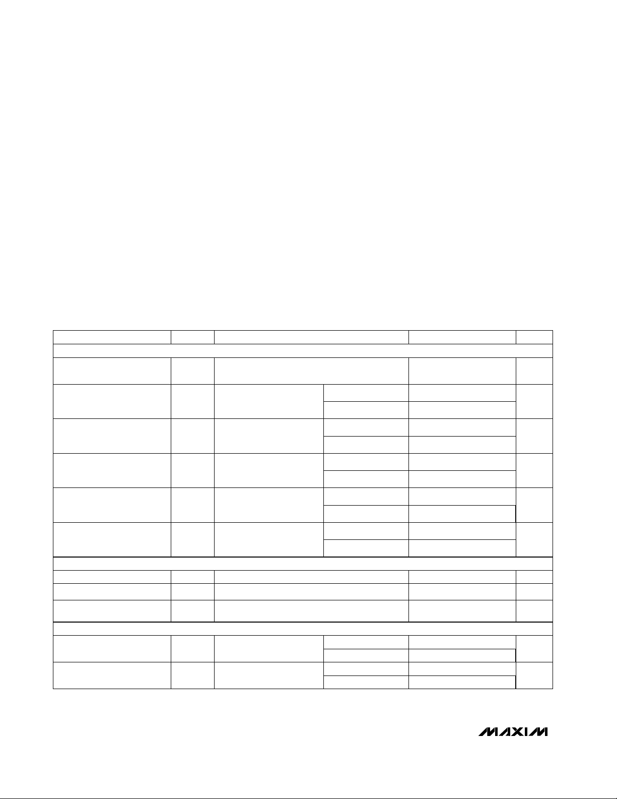
ELECTRICAL CHARACTERISTICS—Single +5V Supply
(V+ = 4.5V to 5.5V, VIH= 2.4V, VIL= 0.8V, TA= T
MIN
to T
MAX
, unless otherwise specified.) (Notes 2, 3)
Note 1: Signals on NO, NC, or COM, exceeding V+ or GND are clamped by internal diodes. Limit forward current to maximum current
rating.
T
A
= +25°C
Turn-Off Time (Note 5) t
OFF
810
ns
TA= +25°C
VIN_ = 0.8V or 2.4V
-0.35 0.35
TA= T
MIN
to T
MAX
TA= +25°C
0.6
TA= T
MIN
to T
MAX
TA= +25°C
3
TA= +25°C
I
COM
= 10mA,
VNOor VNC= 0 to V+,
V+ = 4.5V
-0.35 0.35
PARAMETER SYMBOL MIN TYP MAX UNITSCONDITIONS
Turn-On Time (Note 5) t
ON
12 15
ns
VNO, VNC= 3V, RL= 300Ω,
C
L
= 35pF, Figure 2
VNO, VNC= 3V, RL= 300Ω,
C
L
= 35pF, Figure 2
Logic Input Current I
IN
-0.1 0.005 0.1
µA
12
Input Logic Low V
IL
0.8
V
TA= T
MIN
to T
MAX
Input Logic High V
IH
2.4
V
18
TA= T
MIN
to T
MAX
COM On-Leakage Current
(Notes 5, 6)
I
COM(ON)
-0.25 0.01 0.25
nA
COM Off-Leakage Current
(Notes 5, 6)
I
COM(OFF)
-0.25 0.01 0.25
nA
TA= T
MIN
to T
MAX
TA= +25°C
-0.35 0.35
TA= T
MIN
to T
MAX
TA= +25°C
Off-Leakage Current
(NO or NC) (Notes 5, 6)
I
NO(OFF)
,
I
NC(OFF)
-0.25 0.01 0.25
nA
V
COM
= 1V, 4.5V;
VNOor VNC= 4.5V, 1V;
V+ = 5.5V
On-Resistance Flatness
(Note 4)
R
FLAT(ON)
0.1 0.4
Ω
I
COM
= 10mA,
VNOor VNC= 0 to V+,
V+ = 4.5V
COM to NO or NC
On-Resistance
R
ON
1.5 2.5
Ω
TA= T
MIN
to T
MAX
Input Voltage Range
V
COM
,
VNO, V
NC
0V+
V
V
COM
= 1V, 4.5V;
V
NO
or VNC= 4.5V, 1V;
V+ = 5.5V
ANALOG SWITCH
SWITCH DYNAMIC CHARACTERISTICS
V+ = 5.5V; V
COM
= 4.5V,
1V; V
NO
or VNC= 4.5V,
1V, or floating
LOGIC INPUT
Page 3
MAX4645/MAX4646
Fast, Low-Voltage, 2.5Ω, SPST,
CMOS Analog Switches
_______________________________________________________________________________________ 3
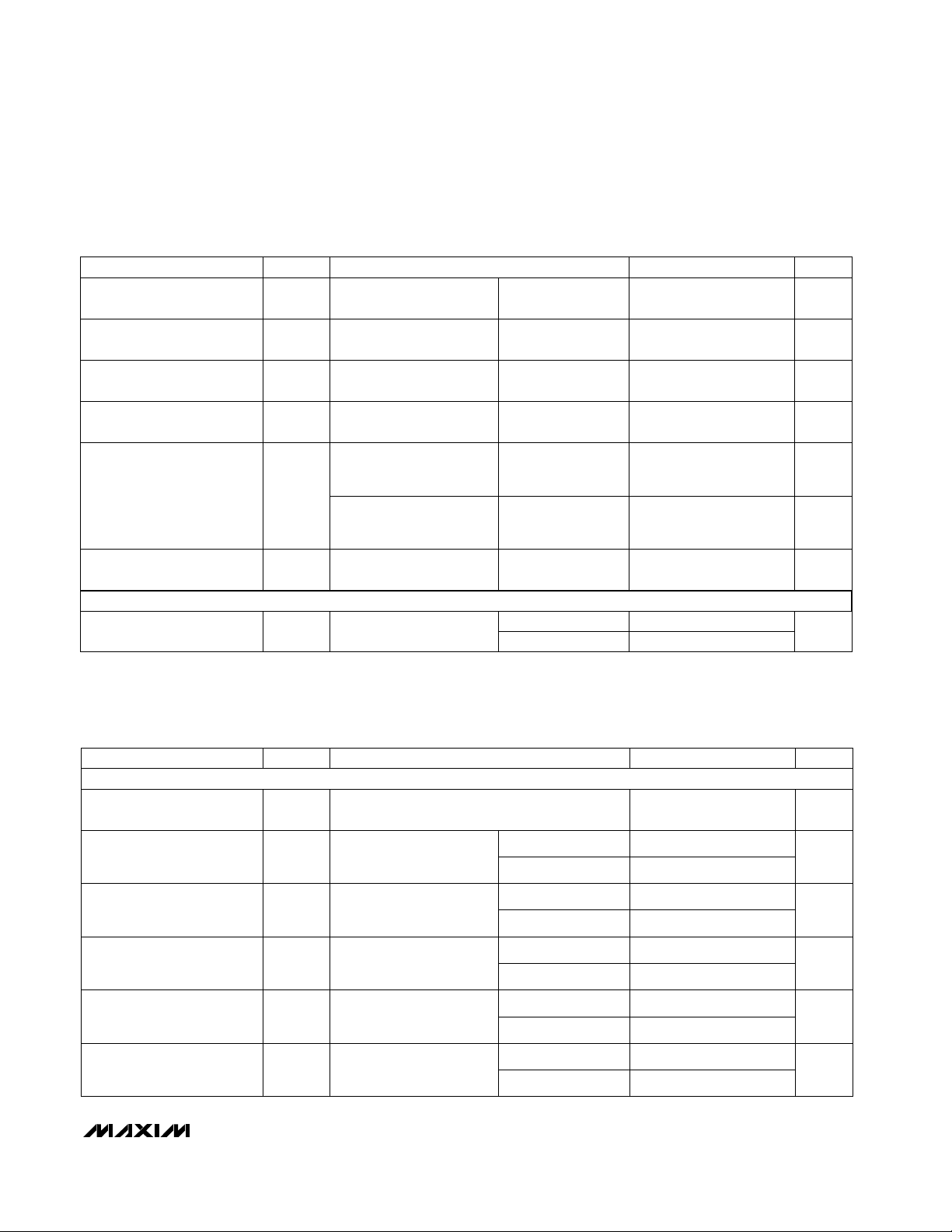
ELECTRICAL CHARACTERISTICS—Single +3V Supply
(V+ = 2.7V to 3.3V, VIH= 2.0V, VIL= 0.4V, TA= T
MIN
to T
MAX
, unless otherwise specified.) (Notes 2, 3)
ELECTRICAL CHARACTERISTICS—Single +5V Supply (continued)
(V+ = 4.5V to 5.5V, VIH= 2.4V, VIL= 0.8V, TA= T
MIN
to T
MAX
, unless otherwise specified.) (Notes 2, 3)
V
0V+
V
COM
,
VNO, V
NC
Input Voltage Range
TA= T
MIN
to T
MAX
Ω
2.5 3.5
R
ON
COM to NO or NC
On-Resistance
I
COM
= 10mA,
V
NO
or VNC= 0 to V+,
V+ = 2.7V
Ω
0.5 0.9
R
FLAT(ON)
On-Resistance Flatness
(Note 4)
V
COM
= 1V, 3V;
VNOor VNC= 3V, 1V;
V+ = 3.3V
nA
-0.25 0.01 0.25
I
NO(OFF)
,
I
NC(OFF)
Off-Leakage Current
(NO or NC) (Notes 5, 6)
TA= +25°C
TA= T
MIN
to T
MAX
-0.35 0.35
TA= +25°C
TA= T
MIN
to T
MAX
V
COM
= 1V, 3V;
V
NO
or VNC= 3V, 1V;
V+ = 3.3V
nA
-0.25 0.01 0.25
I
COM(OFF)
COM Off-Leakage Current
(Notes 5, 6)
V+ = 3.3V; V
COM
= 1V, 3V;
VNOor VNC= 1V,
3V or floating
nA
-0.25 0.01 0.25
I
COM(ON)
COM On-Leakage Current
(Notes 5, 6)
CONDITIONS UNITSMIN TYP MAXSYMBOLPARAMETER
-0.35 0.35
I
COM
= 10mA,
V
NO
or VNC= 0 to V+,
V+ = 2.7V
TA= +25°C
4.5
TA= +25°C
TA= T
MIN
to T
MAX
1
TA= +25°C
TA= T
MIN
to T
MAX
-0.35 0.35
ANALOG SWITCH
-75
dB
VNO= VNC= 1V
RMS
,
RL= 50Ω, CL= 5pF,
f = 1MHz, Figure 4
TA= +25°C
PARAMETER SYMBOL MIN TYP MAX
1.0
UNITS
Positive Supply Current I+
0.0001
V+ = 5.5V, VIN= 0 or V+,
all channels on or off
Total Harmonic Distortion THD
0.014
%
RL= 600Ω, 5V
P-P
,
f = 20Hz to 20kHz
CONDITIONS
TA= T
MIN
to T
MAX
TA= +25°C
TA= +25°C
Off-Isolation (Note 7) V
ISO
-55
dB
VNO= VNC= 1V
RMS
,
RL= 50Ω, CL= 5pF,
f = 10MHz, Figure 4
COM On-Capacitance C
COM
38
pF
V
COM
= VNO, VNC= GND
f = 1MHz, Figure 5
COM Off-Capacitance C
COM
17
pF
V
COM
= GND, f = 1MHz,
Figure 5
NO or NC Capacitance C
OFF
17
pF
VNO, VNC= GND,
f = 1MHz, Figure 5
Charge Injection Q
5
pC
V
GEN
= 2V, CL= 1.0nF,
R
GEN
= 0, Figure 3
TA= +25°C
TA= +25°C
TA= +25°C
TA= +25°C
TA= +25°C
µA
POWER SUPPLY
Page 4
MAX4645/MAX4646
Fast, Low-Voltage, 2.5Ω, SPST,
CMOS Analog Switches
4 _______________________________________________________________________________________
Note 2: The algebraic convention, where the most negative value is a minimum and the most positive value is a maximum, is used
in this data sheet.
Note 3: SOT packages are 100% production tested at +25°C. Limits at the maximum rated temperature are guaranteed by
correlation.
Note 4: Flatness is defined as the difference between the maximum and the minimum value of on-resistance as measured over the
specified analog signal ranges.
Note 5: Guaranteed by design.
Note 6: Leakage parameters are 100% tested at +85°C and guaranteed by correlation at +25°C.
Note 7: Off-Isolation = 20log
10(VCOM / VNO
), V
COM
= output, VNO= input to off switch.
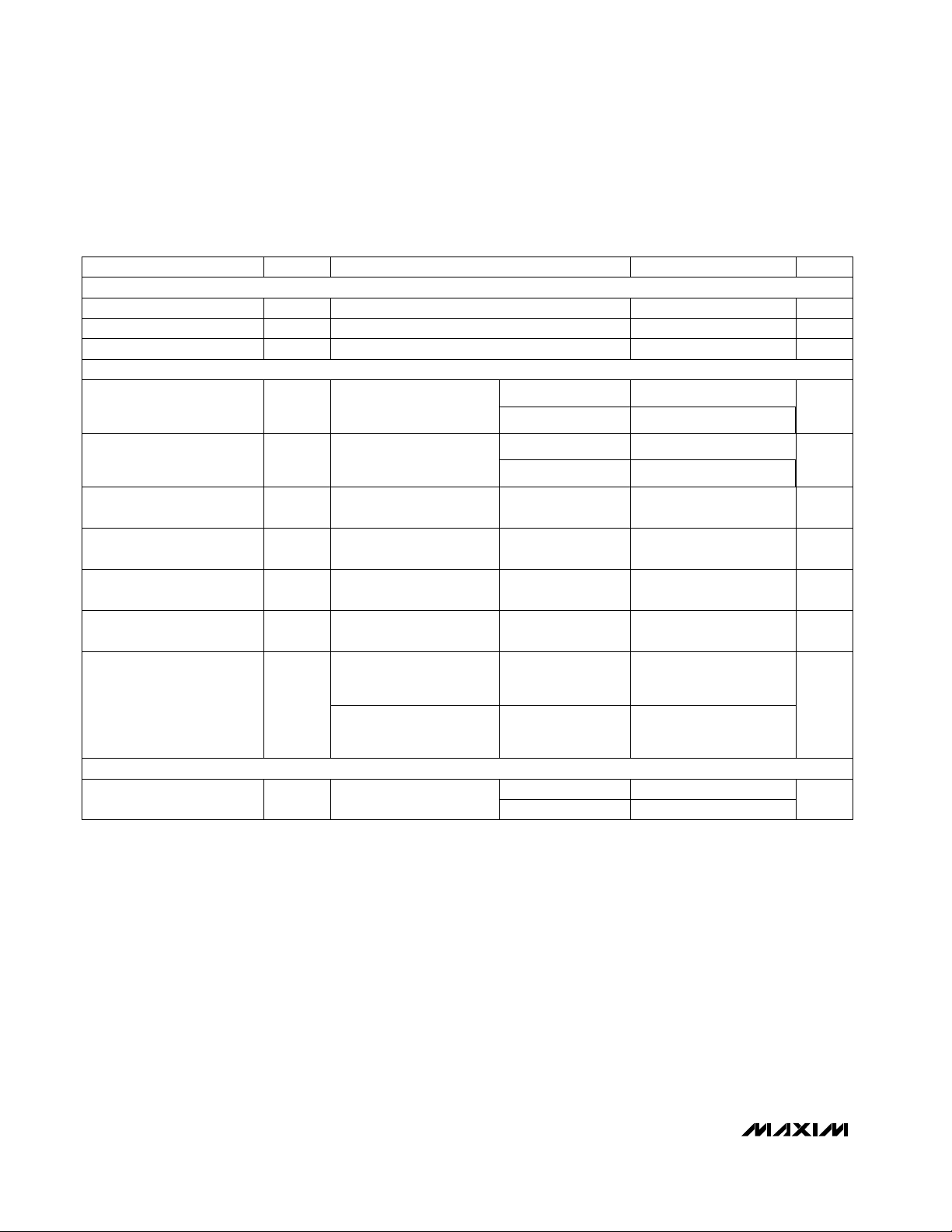
ELECTRICAL CHARACTERISTICS—Single +3V Supply (continued)
(V+ = 2.7V to 3.3V, VIH= 2.0V, VIL= 0.4V, TA= T
MIN
to T
MAX
, unless otherwise specified.) (Notes 2, 3)
-75
TA= +25°C
Turn-Off Time (Note 5) t
OFF
810
ns
TA= +25°C
VIN_ = 0.4V or 2.0V
VNO= VNC= 1V
RMS
,
RL= 50Ω, CL= 5pF,
f = 1MHz, Figure 4
TA= +25°C
PARAMETER SYMBOL MIN TYP MAX
1.0
UNITS
Positive Supply Current I+
0.0001
µA
V+ = 3.3V, VIN= 0 or V+,
all channels on or off
CONDITIONS
TA= T
MIN
to T
MAX
TA= +25°C
Off-Isolation (Note 7) V
ISO
-55
dB
VNO= VNC= 1V
RMS
,
RL= 50Ω, CL= 5pF,
f = 10MHz, Figure 4
COM On-Capacitance C
COM
38
pF
V
COM
= VNO, VNC= GND,
f = 1MHz, Figure 5
COM Off-Capacitance C
COM
17
pF
V
COM
= GND, f = 1MHz,
Figure 5
NO or NC Capacitance C
OFF
17
pF
VNO, VNC= GND,
f = 1MHz, Figure 5
Charge Injection Q
4
pC
V
GEN
= 1.5V, CL= 1.0nF,
R
GEN
= 0, Figure 3
TA= +25°C
TA= +25°C
TA= +25°C
TA= +25°C
TA= +25°C
Turn-On Time (Note 5) t
ON
12 15
ns
VNO, VNC= 2.0V,
RL= 300Ω,CL= 35pF,
Figure 2
VNO, VNC= 2.0V,
RL= 300Ω,CL= 35pF,
Figure 2
Logic Input Current I
IN
-1 0.005 1
µA
13
Input Logic Low V
IL
0.4
V
TA= T
MIN
to T
MAX
Input Logic High V
IH
2.0
V
20
TA= T
MIN
to T
MAX
LOGIC INPUT
SWITCH DYNAMIC CHARACTERISTICS
POWER SUPPLY
Page 5
MAX4645/MAX4646
Fast, Low-Voltage, 2.5Ω, SPST,
CMOS Analog Switches
_______________________________________________________________________________________ 5
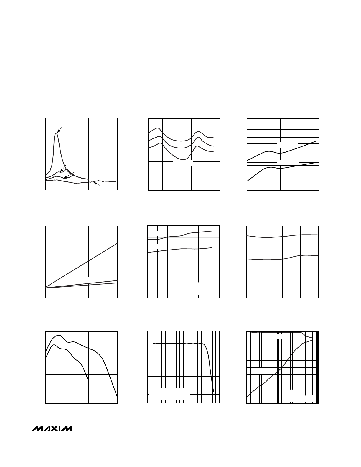
-10
0
10
20
30
40
50
60
70
012345
SUPPLY CURRENT vs. SUPPLY VOLTAGE
AND TEMPERATURE
MAX4645/6-04
SUPPLY VOLTAGE (V)
SUPPLY CURRENT (nA)
TA = +85°C
TA = +25°C
TA = -40°C
0
4
2
8
6
10
12
-40 0 20-20 40 60 10080
TURN-ON/TURN-OFF TIME
vs. TEMPERATURE
MAX4645/6-05
TEMPERATURE (°C)
t
ON
/t
OFF
(ns)
tON
t
OFF
V
COM
= 3V
V+ = 5V
0
2
1
4
3
5
6
7
8
1.0 2.0 2.51.5 3.0 3.5 4.0 4.5 5.0
TURN-ON/TURN-OFF TIME
vs. V
COM
MAX4645/6-06
V
COM
(V)
t
ON
/t
OFF
(ns)
tON
t
OFF
V+ = 5V
0
4
2
8
6
10
12
021 345
ON-RESISTANCE vs. V
COM
AND SUPPLY VOLTAGE
MAX4645/6-01
V
COM
(V)
R
ON
(Ω)
V+ = 1.8V
V+ = 2.5V
V+ = 3V
V+ = 5V
0
0.5
1.5
1.0
2.0
2.5
021345
ON-RESISTANCE vs. V
COM
AND TEMPERATURE
MAX4645/6-02
V
COM
(V)
R
ON
(Ω)
TA = +85°C
TA = +25°C
TA = -40°C
V+ = 4.5V
1
-40 -20 0 20 40 60 80
0.01
0.1
ON/OFF-LEAKAGE CURRENT
vs. TEMPERATURE
MAX4645/6-03
TEMPERATURE (°C)
ON/OFF-LEAKAGE (nA)
ON-LEAKAGE
OFF-LEAKAGE
V+ = 5.5V
__________________________________________Typical Operating Characteristics
(TA = +25°C, unless otherwise noted.)
021 345
CHARGE INJECTION vs. V
COM
MAX4645/6-07
V
COM
(V)
CHARGE INJECTION (pC)
V+ = 5V
V+ = 3V
30
25
20
15
10
5
0
-5
-20
-15
-10
0.016
0.014
0.012
0.010
0.008
0.006
0.004
0.002
0
0.01 1 100.1 100
MAX4645/6-08
FREQUENCY (kHz)
THD (%)
TOTAL HARMONIC DISTORTION
vs. FREQUENCY
INPUT IMPEDANCE = 600Ω
f = 20Hz TO 50kHz
0
-100
0.1 1 10 100 1000
FREQUENCY RESPONSE
-80
MAX4645/6-09
FREQUENCY (MHz)
RESPONSE (dB)
-60
-40
-20
-30
-50
-70
-90
-10
V+ = 5V
50Ω IN AND OUT
ON-LOSS
OFF-LOSS
Page 6
MAX4645/MAX4646
Fast, Low-Voltage, 2.5Ω, SPST,
CMOS Analog Switches
6 _______________________________________________________________________________________
Detailed Description
The MAX4645/MAX4646 are low 2.5Ω max on-resistance (at V+ = 5V), low-voltage analog switches that
operate from a +1.8V to +5.5V single supply. CMOS
switch construction allows processing analog signals
that are within the supply voltage range (GND to V+).
Applications Information
Proper power-supply sequencing is recommended for
all CMOS devices. Do not exceed the absolute maximum ratings because stresses beyond the listed ratings can cause permanent damage to the devices.
Always sequence V+ on first, followed by the logic
inputs, NO, or COM. If power-supply sequencing is not
possible, add two small signal diodes (D1, D2) in series
with the supply pins for overvoltage protection (Figure
1). Adding these diodes reduces the analog signal by
one diode drop below V+ and one diode drop above
GND, but does not affect the low switch resistance and
low leakage characteristics of the device. Device operation is unchanged, and the difference between V+ and
GND should not exceed 6V.
Although it is not required, power-supply bypassing
improves noise margin and prevents switching noise
from propagating from the V+ supply to other components. A 0.1µF capacitor, connected from V+ to GND,
is adequate for most applications.
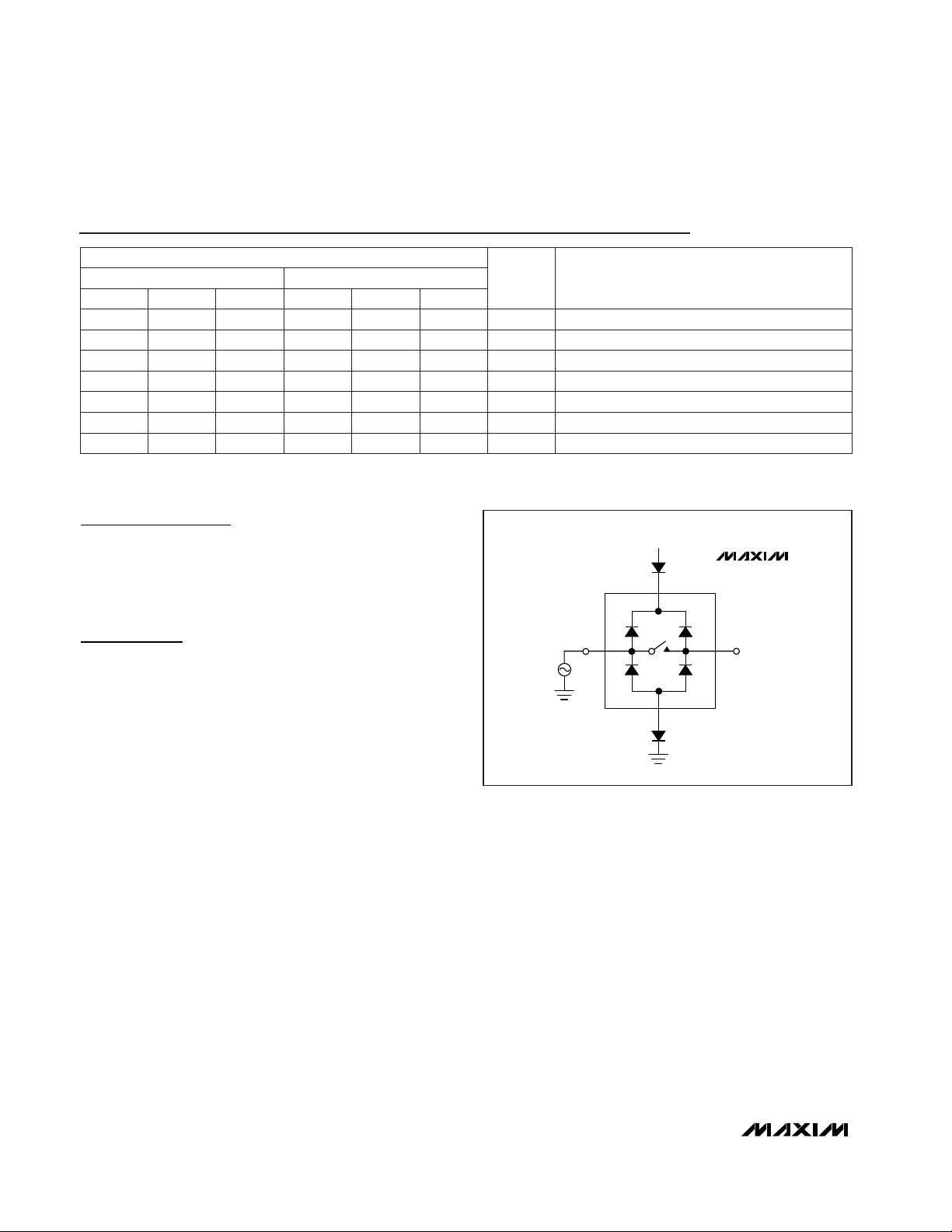
Pin Description
POSITIVE SUPPLY
COM
NO
GND
V
g
V+
MAX4645
MAX4646
D2
D1
Figure 1. Overvoltage Protection Using Two External Blocking
Diodes
V+
COM
NO
NC
GND
IN
N.C.5
6
SOT23-6
2
—
3
4
1
4
µMAX
1
—
8
7
6
2, 3, 5—
5
SOT23-5
—
2
3
4
1
2, 3, 5
4
µMAX
8
—
7
6
1
—
5 6
SOT23-5 SOT23-6
Positive Supply Voltage
1 Analog Switch Common Terminal
2 — Analog Switch Normally Open Terminal
— 2 Analog Switch Normally Closed Terminal
3 3 Ground
4 4 Logic Control Input
1
5 No Connection. Not internally connected.
MAX4646MAX4645
NAME
PIN
FUNCTION
Page 7
MAX4645/MAX4646
Fast, Low-Voltage, 2.5Ω, SPST,
CMOS Analog Switches
_______________________________________________________________________________________ 7
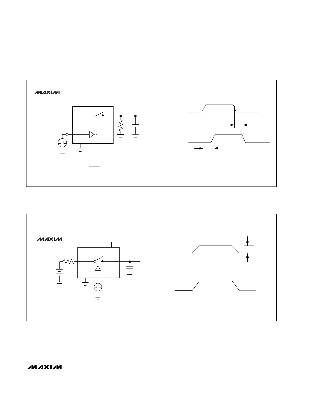
V
GEN
GND
NO
C
L
V
OUT
V+
V
OUT
∆V
OUT
Q = (∆V
OUT
)(CL)
COM
OFF
ON
OFF
IN
V
IN
V+
R
GEN
IN
MAX4645
MAX4646
Figure 3. Charge Injection
tr < 5ns
tf < 5ns
50%
0
LOGIC
INPUT
R
L
300Ω
NO
GND
C
L
INCLUDES FIXTURE AND STRAY CAPACITANCE.
V
OUT
= V
COM (
R
L
)
RL + R
ON
SWITCH
INPUT
IN
V+
t
OFF
0
COM
SWITCH
OUTPUT
0.9 × V
0UT
0.9 × V
OUT
t
ON
V
OUT
SWITCH
OUTPUT
LOGIC
INPUT
LOGIC INPUT WAVEFORMS INVERTED FOR SWITCHES
THAT HAVE THE OPPOSITE LOGIC SENSE.
V+
C
L
35pF
V+
V
OUT
MAX4645
MAX4646
V
COM
Figure 2. Switching Time
Test Circuits/Timing Diagrams
Page 8

MAX4645/MAX4646
Fast, Low-Voltage, 2.5Ω, SPST,
CMOS Analog Switches
8 _______________________________________________________________________________________
_________________________________Test Circuits/Timing Diagrams (continued)
IN
V
IL
OR
V
IH
SIGNAL
GENERATOR 0dBm
V+
10nF
ANALYZER
NO
R
L
GND
COM
V+
MAX4645
MAX4646
Figure 4. Off-Isolation/On-Channel Bandwidth
CAPACITANCE
METER
NC OR
NO
COM
GND
IN
V
IL
OR
V
IH
10nF
V+
f = 1MHz
V+
MAX4645
MAX4646
Figure 5. Channel Off/On-Capacitance
Chip Information
TRANSISTOR COUNT: 50
TOP VIEW
NO
IN
GND
1
6
V+
COM
MAX4645
SOT23-6
2 5
3
4
NC
IN
GND
1
6
V+
N.C.
N.C.
COM
MAX4646
SOT23-6
25
3
4
N.C. = NOT INTERNALLY CONNECTED
SWITCHES SHOWN FOR LOGIC 0 INPUT.
IN
N.C.
N.C.
V+
1
2
8
7
NO
GND
N.C.
COM
MAX4645
3
4
6
5
IN
N.C.
N.C.
V+
1
2
8
7
NC
GND
N.C.
COM
MAX4646
µMAX
3
4
6
5
µMAX
INPUT
0
1
SWITCH STATE
MAX4645
OFF
ON
MAX4646
ON
OFF
PIN 6
6
XYZA
4
123
NOTE: SOT23-6
PACKAGE
HAS LETTERING
NEAREST PIN 6.
5
Pin Configurations/Functional Diagrams/Truth Tables (continued)
Page 9

MAX4645/MAX4646
Fast, Low-Voltage, 2.5Ω, SPST,
CMOS Analog Switches
_______________________________________________________________________________________ 9
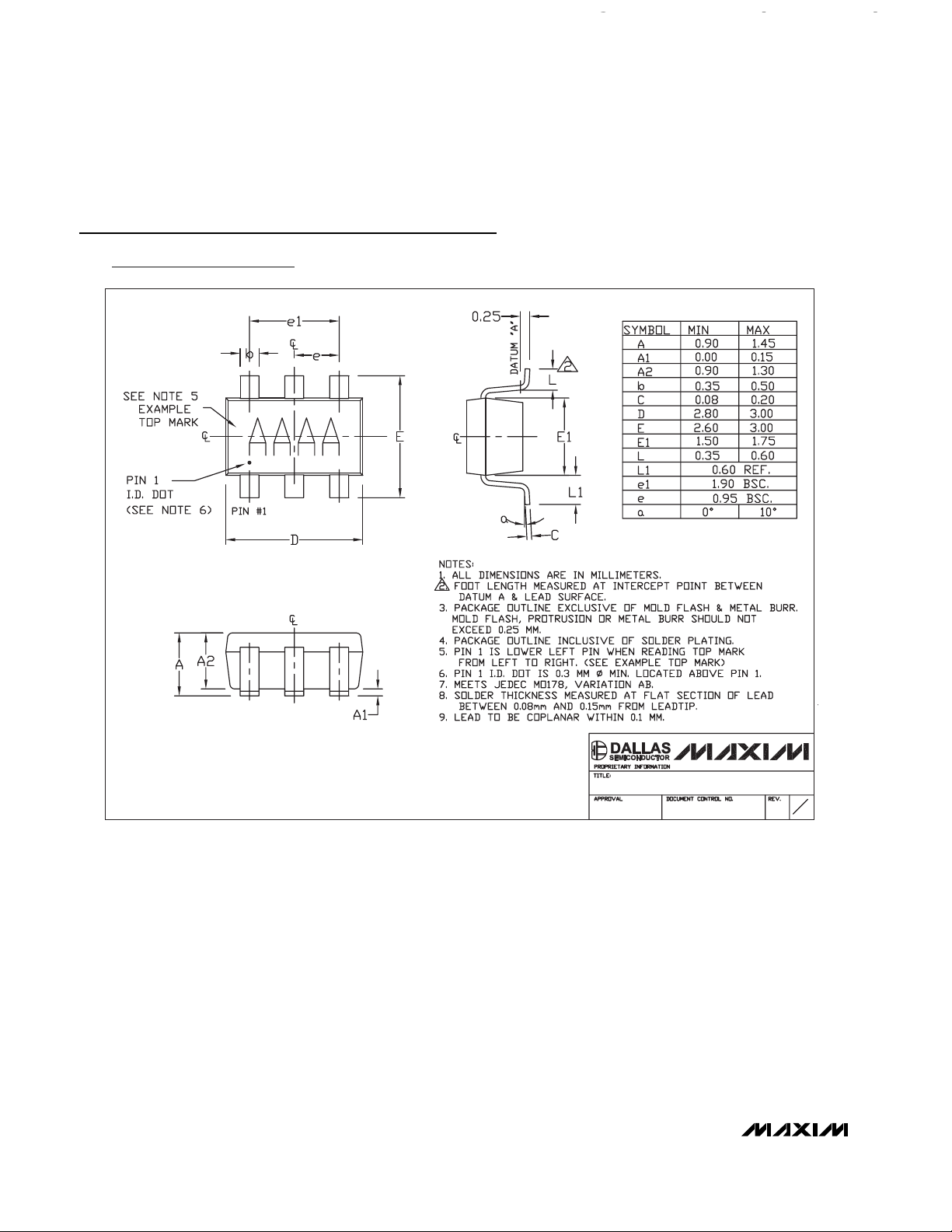
SOT-23 5L .EPS
E
1
1
21-0057
PACKAGE OUTLINE, SOT-23, 5L
Package Information
(The package drawing(s) in this data sheet may not reflect the most current specifications. For the latest package outline information
go to www.maxim-ic.com/packages
.)
Page 10
MAX4645/MAX4646
Fast, Low-Voltage, 2.5Ω, SPST,
CMOS Analog Switches
10 ______________________________________________________________________________________
6LSOT.EPS
F
1
1
21-0058
PACKAGE OUTLINE, SOT-23, 6L
g()
Package Information (continued)
(The package drawing(s) in this data sheet may not reflect the most current specifications. For the latest package outline information
go to www.maxim-ic.com/packages
.)
Page 11

MAX4645/MAX4646
Fast, Low-Voltage, 2.5Ω, SPST,
CMOS Analog Switches
8LUMAXD.EPS
PACKAGE OUTLINE, 8L uMAX/uSOP
1
1
21-0036
J
REV.DOCUMENT CONTROL NO.APPROVAL
PROPRIETARY INFORMATION
TITLE:
MAX
0.043
0.006
0.014
0.120
0.120
0.198
0.026
0.007
0.037
0.0207 BSC
0.0256 BSC
A2
A1
c
e
b
A
L
FRONT VIEW
SIDE VIEW
E H
0.6±0.1
0.6±0.1
ÿ 0.50±0.1
1
TOP VIEW
D
8
A2
0.030
BOTTOM VIEW
1
6∞
S
b
L
H
E
D
e
c
0∞
0.010
0.116
0.116
0.188
0.016
0.005
8
4X S
INCHES
-
A1
A
MIN
0.002
0.950.75
0.5250 BSC
0.25 0.36
2.95 3.05
2.95 3.05
4.78
0.41
0.65 BSC
5.03
0.66
6∞0∞
0.13 0.18
MAX
MIN
MILLIMETERS
- 1.10
0.05 0.15
α
α
DIM
Note: The MAX4645/MAX4646 do not have an exposed paddle.
Maxim cannot assume responsibility for use of any circuitry other than circuitry entirely embodied in a Maxim product. No circuit patent licenses are
implied. Maxim reserves the right to change the circuitry and specifications without notice at any time.
11 __________________Maxim Integrated Products, 120 San Gabriel Drive, Sunnyvale, CA 94086 (408) 737-7600
© 2004 Maxim Integrated Products Printed USA is a registered trademark of Maxim Integrated Products.
Package Information (continued)
(The package drawing(s) in this data sheet may not reflect the most current specifications. For the latest package outline information
go to www.maxim-ic.com/packages
.)
 Loading...