

Page 1
19-1657; Rev 1; 1/11
High-Speed, Low-Voltage, 4Ω,
SPDT CMOS Analog Switch
General Description
The MAX4644 is a single-pole/double-throw (SPDT)
switch that operates from a single supply ranging from
+1.8V to +5.5V. It provides low 4Ω on-resistance (RON)
as well as 1Ω R
flatness over the entire analog-signal
ON
range. The MAX4644 offers fast switching times of less
than 20ns while ensuring break-before-make operation.
It typically consumes only 0.01μW of quiescent power,
making it suitable for use in low-power, portable applications.
The MAX4644’s features include low leakage currents
over the entire temperature range, TTL/CMOS-compatible digital logic, and excellent AC characteristics. It is
packaged in either a small 8-pin μMAX
®
or a tiny 6-pin
SOT23.
Applications
Battery-Operated Equipment
Audio and Video Signal Routing
Low-Voltage Data-Acquisition Systems
Sample-and-Hold Circuits
Communications Circuits
ËMAX is a registered trademark of Maxim Integrated
Products, Inc.
Features
♦ +1.8V to +5.5V Single-Supply Operation
♦ Rail-to-Rail Analog-Signal Range
♦ Guaranteed R
ON
4Ω max (+5V Supply)
8Ω max (+3V Supply)
♦ +1.8V Operation
RON30Ω (typ) Over Temperature
t
18ns (typ), t
ON
OFF
12ns typ
♦ Guaranteed RONFlatness: 0.75Ω (typ) (+5V Supply)
♦ Guaranteed RONMatch Between Channels:
0.1Ω typ (+5V Supply)
♦ Low Leakage (< 0.35nA) Over Entire Temperature
Range
♦ Excellent AC Characteristics
Low Crosstalk: -82dB at 1MHz
High Off-Isolation: -80dB at 1MHz
0.018% Total Harmonic Distortion
♦ Low Power Consumption: < 0.01µW
Ordering Information
PART TEMP. RANGE
MAX4644EUT+T -40°C to +85°C 6 SOT23 AAHQ
MAX4644EUA+T -40°C to +85°C 8 μMAX —
+
Denotes a lead(Pb)-free/RoHS-compliant package.
T = Tape and reel.
PINPACKAGE
TOP
MARK
MAX4644
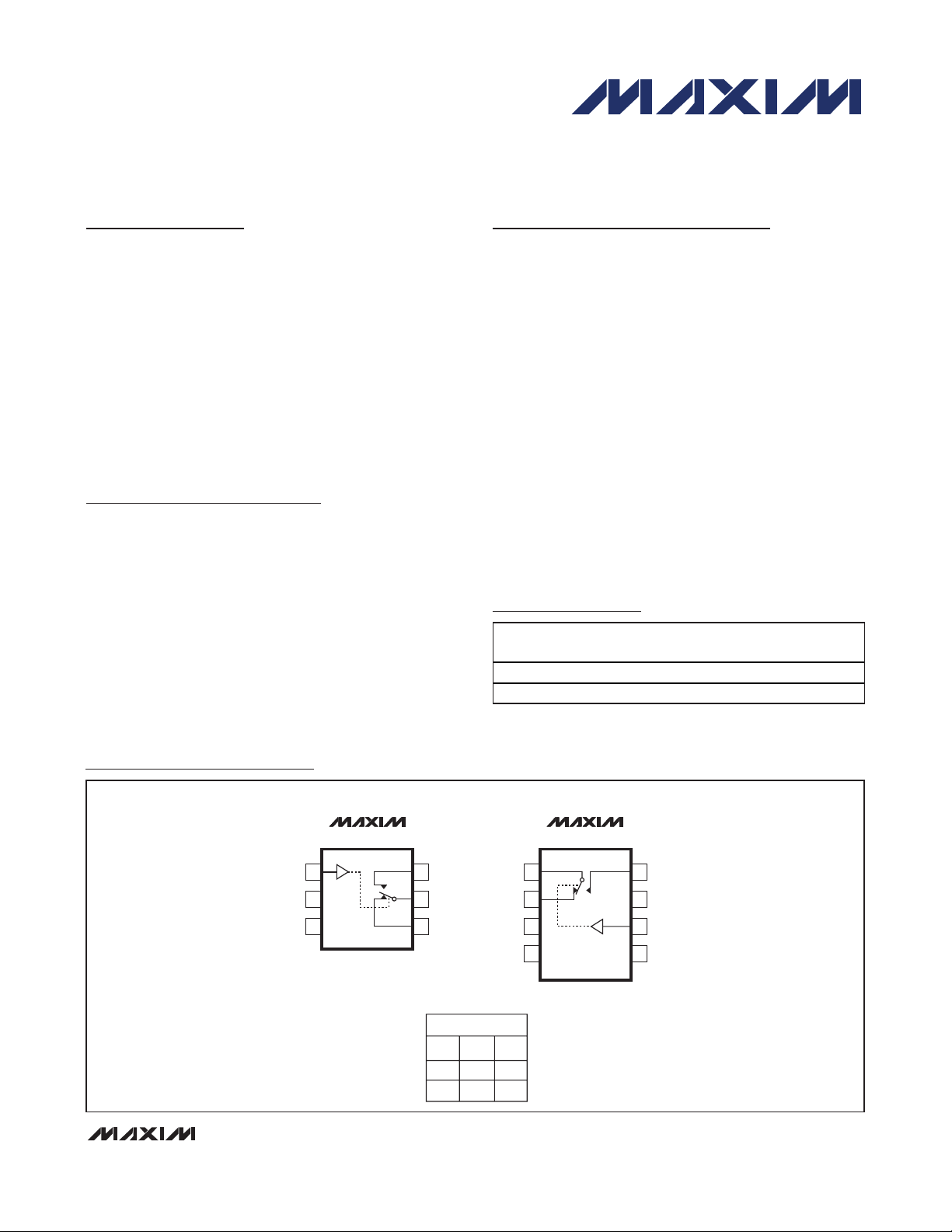
Pin Configurations/Functional Diagrams/Truth Table
TOP VIEW
MAX4644
1
IN
2
V+
3
GND
SOT23-6
________________________________________________________________
6
NO
COM
5
4
NC
IN
0
1
MAX4644
NC NO
ON
OFF
COM
NC
GND
V+
OFF
ON
For pricing, delivery, and ordering information, please contact Maxim Direct at 1-888-629-4642,
or visit Maxim’s website at www.maxim-ic.com.
MAX4644
1
2
3
4
μMAX
8
NO
N.C.
7
6
IN
N.C.
5
Maxim Integrated Products
1
Page 2
High-Speed, Low-Voltage, 4Ω,
SPDT CMOS Analog Switch
ABSOLUTE MAXIMUM RATINGS
(All voltages referenced to GND.)
V+ .............................................................................-0.3V to +6V
IN, COM, NO, NC (Note 1) ...........................-0.3V to (V+ + 0.3V)
Continuous Current (any terminal)....................................±20mA
Continuous Current (NO, NC, and COM) .........................±50mA
Peak Current (NO, NC, and COM, pulsed at 1ms,
10% duty cycle)......................................................... ±100mA
Continuous Power Dissipation (T
6-Pin SOT23 (derate 8.70mW/°C above +70°C)........ 696mW
8-Pin μMAX (derate 4.5mW/°C above +70°C) ........... 362mW
Operating Temperature Range ...........................-40°C to +85°C
Junction Temperature......................................................+150°C
Storage Temperature Range .............................-65°C to +150°C
Lead Temperature (soldering, 10s) ................................ +300°C
Soldering Temperature (reflow) ...................................... +260°C
= +70°C)
A
MAX4644
Note 1: Signals on NO, NC, COM, or IN exceeding V+ or GND are clamped by internal diodes. Limit forward-diode current to maximum
current rating.
Stresses beyond those listed under “Absolute Maximum Ratings” may cause permanent damage to the device. These are stress ratings only, and functional
operation of the device at these or any other conditions beyond those indicated in the operational sections of the specifications is not implied. Exposure to
absolute maximum rating conditions for extended periods may affect device reliability.
ELECTRICAL CHARACTERISTICS—Single +5V Supply
(V+ = +4.5V to +5.5V, V
ANALOG SWITCH
Analog-Signal Range
INH
= 2.4V, V
= 0.8V, TA= T
INL
V
,
COM
V
,
NO
V
NC
MIN
to T
, unless otherwise noted. Typical values are at TA= +25°C.)
MAX
CONDITIONS
UNITSMIN TYP MAXSYMBOLPARAMETER
V0V+
On-Resistance
On-Resistance Match
Between Channels (Note 2)
On-Resistance Flatness
(Note 3)
NO, NC Off-Leakage
Current (Note 4)
COM Off-Leakage Current
(Note 4)
COM On-Leakage Current
(Notes 4, 5)
DIGITAL INPUTS
DIGITAL INPUTS
Input-Logic High
Input-Logic Low
Input Current
R
ON
ΔR
ON
R
FLAT
I
NO(OFF)
I
NC(OFF)
I
COM(OFF)
I
COM(ON)
IH
IL
IN
V+ = 4.5V, I
10mA, VNOor
V
= 0 to V+
NC
V+ = 4.5V, I
10mA, VNOor
V
= 0 to V+
NC
V+ = 4.5V, I
10mA, V
V
= 0 to V+
NC
V+ = 5.5V, V
,
1V or 4.5V, V
= 4.5V or 1V
V
NC
V+ = 5.5V, V
1V or 4.5V, V
V
= 4.5V or 1V
NC
V+ = 5.5V, V
1V or 4.5V
VIN= 0.8V or 2.4V
NO
COM
COM
COM
or
COM
NO
COM
NO
COM
=
TA= +25°C
2.5 4
Ω
4.75
=
TA= T
MIN
TA= +25°C
to T
MAX
0.1
Ω
0.4
=
TA= T
MIN
TA= +25°C
to T
MAX
0.75 1
Ω
1.2
nA
nA
nA
=
TA= T
TA= +25°C
MIN
to T
MAX
-0.25 0.01 0.25
or
-0.35 0.35TA= T
-0.25 0.01 0.25
=
MIN
TA= +25°C
to T
MAX
or
-0.35 0.35TA= T
-0.25 0.01 0.25
-0.35 0.35
=
MIN
TA= +25°C
TA= T
MIN
to T
to T
MAX
MAX
V2.4V
V0.8V
μA-0.1 0.005 0.1I
2 _______________________________________________________________________________________
Page 3
High-Speed, Low-Voltage, 4Ω,
SPDT CMOS Analog Switch
ELECTRICAL CHARACTERISTICS —Single +5V Supply (continued)
(V+ = +4.5V to +5.5V, V
DYNAMIC
Turn-On Time (Note 4)
Turn-Off Time (Note 4)
Break-Before-Make (Note 4)
NO, NC Off-Capacitance
Switch On-Capacitance
Off-Isolation (Note 6)
Crosstalk (Note 7)
SUPPLY
INH
= 2.4V, V
C
= 0.8V, TA= T
INL
t
ON
t
OFF
t
BBM
NO(OFF),
C
NC(OFF)
(ON)
V
ISO
V
CT
to T
MIN
, unless otherwise noted. Typical values are at TA= +25°C.)
MAX
CONDITIONS
RL= 300Ω; CL=
TA= +25°C
35pF; VNO, VNC= 3V;
Figure 2
RL= 300Ω; CL=
35pF; V
, VNC= 3V;
NO
Figure 2
RL= 300Ω;
TA= T
TA= +25°C
TA= T
TA= +25°C
MIN
MIN
to T
to T
CL= 35pF; VNOor
V
= +3V; Figure 2
NC
V
= 0V, R
GEN
TA= T
= 0V, CL= 1nF, Figure 4
GEN
MIN
to T
NO or NC = GND, f = 1MHz, Figure 5
f = 1MHz, Figure 5
CL= 5pF, RL= 50Ω,
Figure 3
CL= 5pF, RL= 50Ω,
Figure 3
f = 10MHz
f = 1MHz
f = 10MHz
f = 1MHz
RL= 600Ω, 0.5Vp-p, f = 20Hz to 20kHz
V+ = 5.5V, VIN= 0V or V+ μA0.001 1.0I+Positive Supply Current
MAX
MAX
MAX
1
11 15
18
35
6
8
-55
-80
-62
-82
MAX4644
UNITSMIN TYP MAXSYMBOLPARAMETER
ns
ns
ns
pC5QCharge Injection
pF12
pF34C
dB
dB
%0.018THDTotal Harmonic Distortion
ELECTRICAL CHARACTERISTICS—Single +3V Supply
(V+ = +2.7V to +3.3V, V
ANALOG SWITCH
Analog-Signal Range
On-Resistance
On-Resistance Match
Between Channels (Note 2)
On-Resistance Flatness
(Note 3)
INH
= 2.0V, V
= 0.4V, TA= T
INL
MIN
to T
, unless otherwise noted. Typical values are at TA= +25°C.)
MAX
CONDITIONS
V
,
COM
V
,
NO
V
NC
ΔR
R
R
FLAT
ON
ON
V+ = 2.7V, I
10mA, V
V
= 0 to V+
NC
NO
V+ = 2.7V, I
10mA, V
V
= 0 to V+
NC
NO
V+ = 2.7V, I
10mA, V
V
= 0 to V+
NC
NO
COM
or
COM
or
COM
or
=
=
=
TA= +25°C
TA= T
MIN
TA= +25°C
TA= T
MIN
TA= +25°C
TA= T
MIN
_______________________________________________________________________________________ 3
to T
to T
to T
MAX
MAX
MAX
UNITSMIN TYP MAXSYMBOLPARAMETER
V0V+
68
Ω
9
0.1
Ω
0.4
1.5 3
Ω
3.5
Page 4

High-Speed, Low-Voltage, 4Ω,
SPDT CMOS Analog Switch
ELECTRICAL CHARACTERISTICS—Single +3V Supply (continued)
(V+ = +2.7V to +3.3V, V
DIGITAL INPUTS
Input-Logic High
Input-Logic Low
Input Current
MAX4644
DYNAMIC
Turn-On Time (Note 4)
INH
= 2.0V, V
= 0.4V, TA= T
INL
IH
IL
IN
t
ON
to T
MIN
VIN= 0.4V or 2.0V
RL= 300Ω; CL=
35pF; VNO, VNC= 2V;
Figure 2
, unless otherwise noted. Typical values are at TA= +25°C.)
MAX
CONDITIONS
TA= +25°C
TA= T
MIN
to T
MAX
UNITSMIN TYP MAXSYMBOLPARAMETER
V2.0V
V0.4V
μA-0.1 0.005 0.1I
14 20
ns
22
RL= 300Ω; CL=
Turn-Off Time (Note 4)
Break-Before-Make (Note 4)
NO, NC Off-Capacitance
Switch On-Capacitance
Off-Isolation (Note 6) dB
Crosstalk (Note 7)
SUPPLY
Note 2: ΔR
Note 3: R
Note 4: Guaranteed by design.
Note 5: On-Leakage performed with voltage applied to COM, with NO and NC left unconnected.
Note 6: Off-Isolation = 20log
Note 7: Crosstalk is measured between the two switches.
= R
ON
ON(MAX)
flatness is defined as the difference between the maximum and minimum value of on-resistance as measured over the
ON
specified analog-signal range.
- R
t
OFF
t
BBM
C
NO(OFF)
C
NC(OFF)
(ON)
V
ISO
V
CT
.
ON(MIN)
/ VI), where VOis V
10(VO
35pF; VNO, VNC= 2V;
Figure 2
RL= 300Ω; CL=
35pF; V
Figure 2
V
GEN
,
NO or NC = GND, f = 1MHz, Figure 5
f = 1MHz, Figure 5 pF34C
CL= 5pF, RL= 50Ω,
Figure 3
CL= 5pF, RL= 50Ω,
Figure 3
V+ = 3.3V, VIN= 0V or V+ μA0.001 1.0I+Positive Supply Current
, VNC= 2V;
NO
= 0V, R
GEN
and VIis either VNCor VNOfrom the network analyzer.
COM
TA= +25°C
TA= T
TA= +25°C
TA= T
= 0V, CL= 1nF, Figure 4
f = 10MHz
f = 1MHz
f = 10MHz
f = 1MHz
MIN
MIN
to T
to T
MAX
MAX
1
4 7.5
8
8
-55
-80
-62
-82
ns
ns
pC5QCharge Injection
pF12
dB
4 _______________________________________________________________________________________
Page 5

High-Speed, Low-Voltage, 4Ω,
SPDT CMOS Analog Switch
(V+ = +5V or +3V, V
= V+, INL = GND, TA= +25°C, unless otherwise noted.)
INH
ON-RESISTANCE vs. V
20
I
= 10mA
COM
15
(Ω)
10
ON
R
5
0
021 345
V+ = 1.8V
V+ = 2.5V
V+ = 3V
V
COM
(V)
CHARGE INJECTION vs. V
140
V+ = 5V
120
100
80
60
40
CHARGE INJECTION (pC)
20
0
021 345
V
(V)
COM
COM
V+ = 5V
COM
MAX4644-01
(Ω)
ON
R
140
120
MAX4644-04
100
80
60
SUPPLY CURRENT (nA)
40
20
Typical Operating Characteristics
ON-RESISTANCE vs. TEMPERATURE
5
I
= 10mA
COM
4
V+ = 3V
3
V+ = 5V
2
1
-40 10-15 35 60 85
TEMPERATURE (°C)
SUPPLY CURRENT vs. SUPPLY VOLTAGE
IN = GND
0
1.8 2.8 3.8 4.8 5.8
SUPPLY VOLTAGE (V)
IN = V+
1000
MAX4644-02
100
LEAKAGE (pA)
10
300
MAX4644-05
250
200
150
100
SUPPLY CURRENT (nA)
50
0
ON-/OFF-LEAKAGE CURRENT
vs. TEMPERATURE
OFF-LEAKAGE
ON-LEAKAGE
1
-40 8535 60-15 10
TEMPERATURE (°C)
SUPPLY CURRENT vs.
TEMPERATURE
IN = GND
V+ = 5V
V+ = 3V
V+ = 1.8V
-40 10-15 35 60 85
TEMPERATURE (°C)
MAX4644
MAX4644-03
MAX4644-06
LOGIC THRESHOLD vs.
SUPPLY VOLTAGE
2.0
1.5
1.0
LOGIC THRESHOLD (V)
0.5
0
1.8 3.42.6 4.2 5.0 5.8
SUPPLY VOLTAGE (V)
_______________________________________________________________________________________
MAX4644-07
SWITCHING TIMES (ns)
SWITCHING TIMES vs. SUPPLY VOLTAGE
15
12
9
6
3
0
2435
SUPPLY VOLTAGE (V)
MAX4644-08
t
ON
t
OFF
SWITCHING TIMES vs. TEMPERATURE
10
V+ = 5V
8
6
4
SWITCHING TIMES (ns)
2
0
-40 35 6010-15 85
t
ON
t
OFF
MAX4644-09
TEMPERATURE (°C)
5
Page 6

High-Speed, Low-Voltage, 4Ω,
0.05
0.01 1 100.1 100
TOTAL HARMONIC DISTORTION
vs. FREQUENCY
MAX4644-11
FREQUENCY (kHz)
THD (%)
0
0.01
0.02
0.03
0.04
V+ = 5V
SPDT CMOS Analog Switch
Typical Operating Characteristics (continued)
(V+ = +5V or +3V, V
= V+, INL = GND, TA= +25°C, unless otherwise noted.)
INH
0
-10
MAX4644
-20
-30
-40
(dB/div)
-50
-60
-70
-80
-90
MAX4644
SOT23
FREQUENCY RESPONSE
V+ = 5V
ON-LOSS
OFF-ISOLATION
0.01 0.1 1 10 100 1000
FREQUENCY (MHz)
µMAX
MAX4644-10
Pin Description
FUNCTIONNAME
1
2
3
—
4
5
6
Note: The switches are bidirectional, which means that a signal can be passed through either side of the on switch. However,
the typical off-capacitances differ as shown in the
6 _______________________________________________________________________________________
6
4
3
5, 7
2
1
8
IN Logic-Controlled Input
V+ Positive Supply Voltage Input. Bypass with a 0.1μF capacitor to GND.
GND Ground
N.C. No Connection. Not internally connected.
NC Analog-Switch Normally Closed Terminal
COM Analog-Switch Common Terminal
NO Analog-Switch Normally Open Terminal
Electrical Characteristics.
Page 7

High-Speed, Low-Voltage, 4Ω,
SPDT CMOS Analog Switch
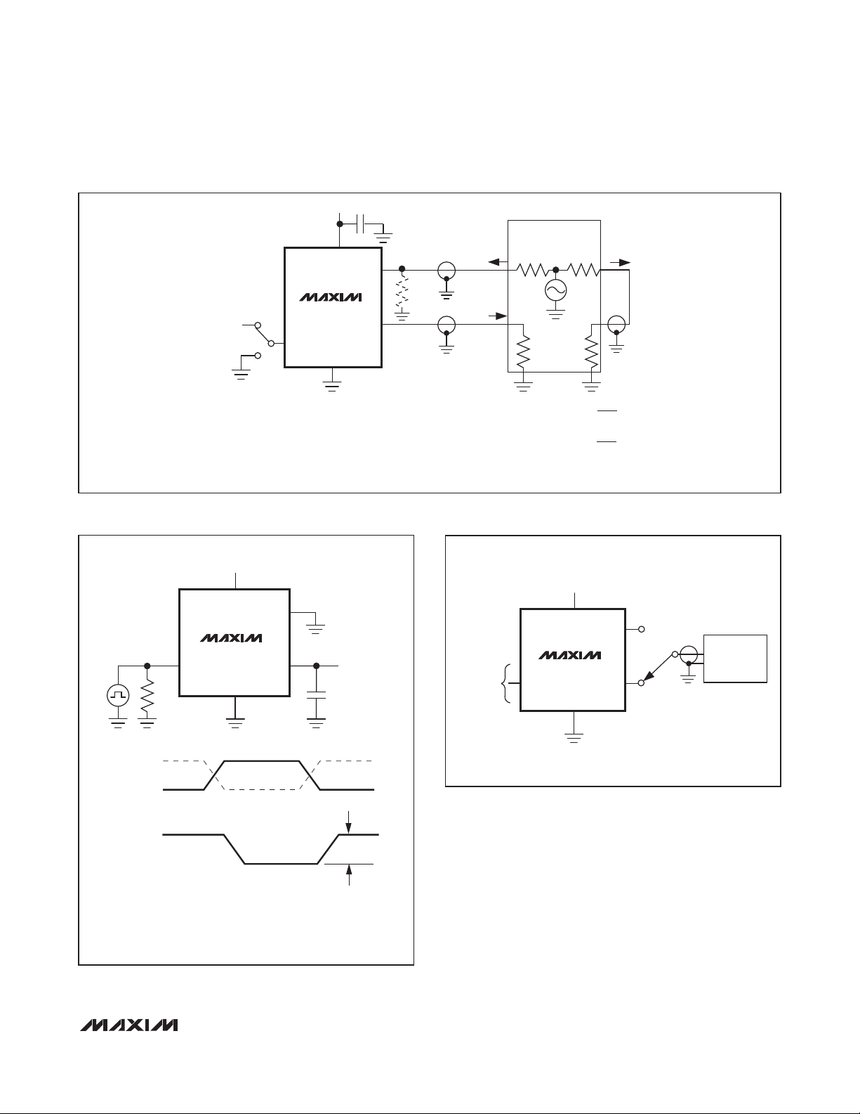
V+
N0, NC
GND
Figure 1. Overvoltage Protection Using External Blocking
Diodes
COM
Applications Information
The MAX4644 operates from a single supply ranging
from +1.8V to +5.5V. The device is guaranteed to be
functional over that supply range, but TTL/CMOS compatibility is only valid for operation using a +5V supply.
All voltage levels are referenced to GND. Positive and
negative DC analog inputs or AC signals can be
accommodated by shifting V+ and GND.
ESD-protection diodes are internally connected
between each analog-signal pin and both V+ and GND.
One of these diodes conducts if any analog signal
exceeds V+ or GND (Figure 1). Virtually all of the analog leakage current comes from the ESD diodes to V+
or GND. Although the ESD diodes on a given signal pin
are identical, and therefore fairly well balanced, they
are reverse biased differently. Each is biased by either
V+ or GND and the analog signal. This means their
leakages will vary as the signal varies. The difference in
the two diode leakages to the V+ and GND pins constitutes the analog-signal-path leakage current. All analog
leakage current flows between each pin and one of the
supply terminals, not to the other switch terminal. This is
why both sides of a given switch can show leakage currents of the same or opposite polarity.
There is no normal current path between the analogsignal paths and V+ or GND. V+ and GND also power
the internal logic and logic-level translators. The logiclevel translators convert the logic level into switched V+
and GND signals to drive the analog signal gates.
Chip Information
PROCESS: BiCMOS
Package Information
For the latest package outline information and land patterns
(footprints), go to www.maxim-ic.com/packages
“+”, “#”, or “-” in the package code indicates RoHS status only.
Package drawings may show a different suffix character, but
the drawing pertains to the package regardless of RoHS status.
PACKAGE
TYPE
6 SOT23 U6+4
8 μMAX U8+1
PACKAGE
CODE
OUTLINE
NO.
21-0058 90-0175
21-0036 90-0092
. Note that a
LAND
PATTERN NO.
MAX4644
_______________________________________________________________________________________ 7
Page 8

High-Speed, Low-Voltage, 4Ω,
SPDT CMOS Analog Switch
V+
V
NO
V
IN
MAX4644
50Ω
V
NC
V
IN
50Ω
V
S
V
IN
50Ω
NO
IN
NC
IN
V
IN
NO
V+
MAX4644
GND
V+
V+
MAX4644
GND
V+
V+
MAX4644
GND
NC OPEN
COM
NO
COM
V
NC
COM
35pF
OPEN
300Ω
VS
300Ω
300Ω
V
COM
35pF
35pF
V
+ 0.5V
IH
IN
0
V
NO
V
COM
0
V
+ 0.5V
IH
IN
0
V
V
COM
V
COM
NC
V
COM
0
V
+ 0.5V
IH
IN
0
V
S
V
COM
0
t
BBM
t
BBM
50% 50%
t
ON
50% 50%
t
OFF
50% 50%
t
BBM
= t
- t
ON(NC)
OFF(NO)
OR
= t
- t
ON(NO)
OFF(NC)
90%
t
OFF
90% 90%
t
90%
tr < 5ns
t
< 5ns
f
90%
ON
90%
t
BBM
Figure 2. Switching Times
8 _______________________________________________________________________________________
Page 9
V+
MEASUREMENTS ARE STANDARDIZED AGAINST
SHORT AT SOCKET TERMINALS. OFF-ISOLATION IS
MEASURED BETWEEN COM AND “OFF” TERMINAL
ON EACH SWITCH. ON-LOSS IS MEASURED BETWEEN
COM AND “ON” TERMINAL ON EACH SWITCH. SIGNAL
DIRECTION THROUGH SWITCH IS REVERSED; WORST
VALUES ARE RECORDED.
Figure 3. Off-Isolation and On-Loss
IN
High-Speed, Low-Voltage, 4Ω,
SPDT CMOS Analog Switch
0.1μF
V+
NETWORK
V+
MAX4644
GND
COM
NO
NC
V
OR
50Ω
V
OUT
ANALYZER
IN
50Ω
MEAS REF
OFF-ISOLATION = 20log
ON-LOSS = 20log
50Ω
50Ω 50Ω
V
OUT
V
IN
V
OUT
V
IN
MAX4644
V+
V+
V
IN
50Ω
V+
V
IN
0
V
OUT
ΔV
IS THE MEASURED VOLTAGE DUE TO CHARGE TRANSFER
OUT
ERROR Q WHEN THE CHANNEL TURNS OFF.
Q = ΔV
OUT x CL
MAX4644
IN
GND
COM
NO
OR
NC
OR VNC = 0V
V
NO
V
C
L
1000pF
ΔV
OUT
OUT
V+
V+
NO
OR
NC
IN
MAX4644
COM
GND
AS
REQUIRED
Figure 5. NO, NC, and COM Capacitance
1MHz
CAPACITANCE
ANALYZER
Figure 4. Charge Injection
_______________________________________________________________________________________ 9
Page 10

High-Speed, Low-Voltage, 4Ω,
SPDT CMOS Analog Switch
Revision History
REVISION
NUMBER
0 3/00 Init ia l release —
1 1/11 Added lead-free parts to the Ordering Information table 1
REVISION
DATE
MAX4644
DESCRIPTION
PAGES
CHANGED
Maxim cannot assume responsibility for use of any circuitry other than circuitry entirely embodied in a Maxim product. No circuit patent licenses are
implied. Maxim reserves the right to change the circuitry and specifications without notice at any time.
10
____________________Maxim Integrated Products, 120 San Gabriel Drive, Sunnyvale, CA 94086 408-737-7600
© 2011 Maxim Integrated Products Maxim is a registered trademark of Maxim Integrated Products, Inc.
 Loading...