Page 1
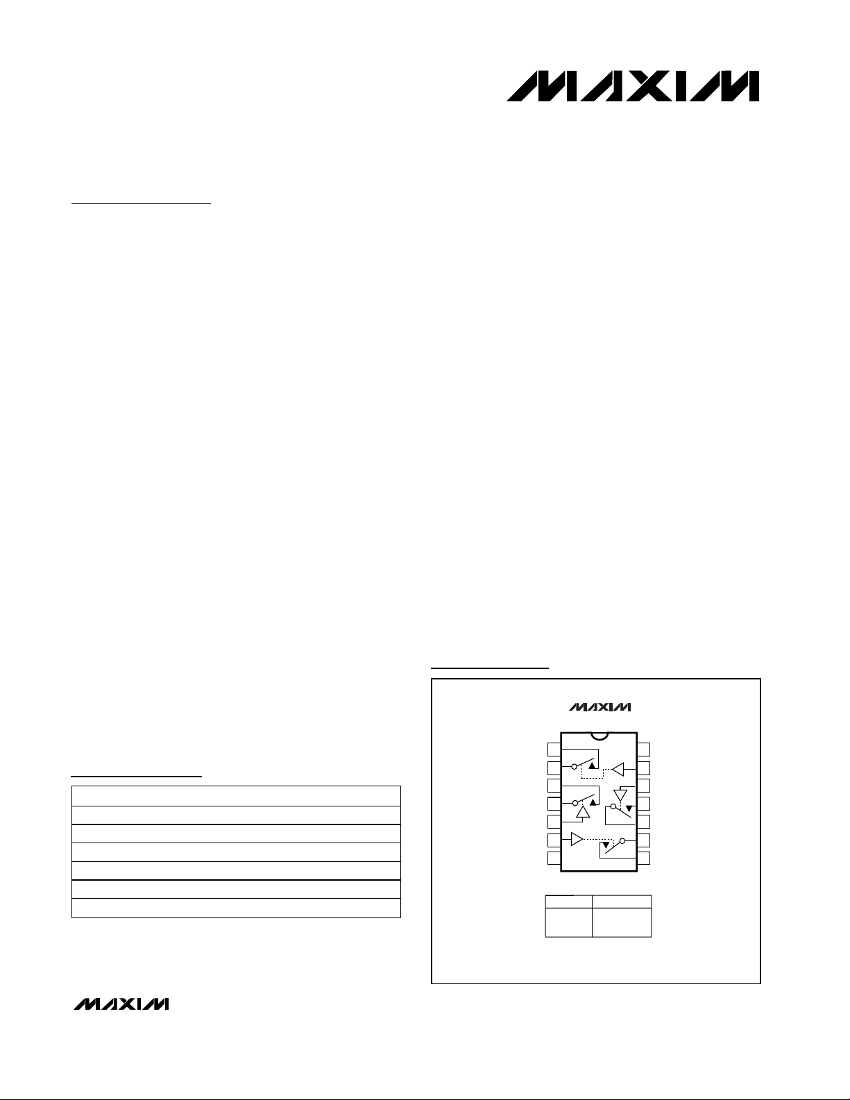
Pin Configurations/Functional Diagrams/Truth Tables
continued at end of data sheet.
General Description
The MAX4620/MAX4630/MAX4640 low-voltage, highESD-protected, quad, single-pole/single-throw (SPST)
analog switches are pin-compatible replacements for
the industry-standard 74HC4066 analog switch. The
normally open (NO) and normally closed (NC) pins are
protected against ±15kV electrostatic discharge (ESD)
without latchup or damage. Each switch can handle
Rail-to-Rail
®
analog signals. The off-leakage current is
0.5nA at +25°C. These analog switches are suitable for
low-distortion audio applications and are the preferred
solution over mechanical relays in automated test
equipment or applications where current switching is
required. They have low power requirements (0.5µW),
require less board space, and are more reliable than
mechanical relays. Each device is controlled by
TTL/CMOS input voltage levels and is bilateral.
These switches feature guaranteed operation from a
+2V to +12V single supply, making them ideal for use
in battery-powered applications. The on-resistance is
70Ω max, matched between switches to 0.5Ω (typ),
and flat (2Ω typ) over the specified signal range.
The MAX4620 has four NO switches, the MAX4630 has
four NC switches, and the MAX4640 has two NO and
two NC switches. These devices are available in 14-pin
TSSOP, SO, and DIP packages.
________________________Applications
Battery-Powered Systems
Audio and Video Signal Routing
Low-Voltage Data-Acquisition Systems
Sample-and-Hold Circuits
Communications Circuits
Relay Replacement
____________________________Features
♦ ESD-Protected NO/NC Pins
±15kV Human Body Model
±15kV IEC 1000-4-2 Air-Gap Discharge
±8kV IEC 1000-4-2 Contact Discharge
♦ Pin Compatible with Industry-Standard 74HC4066,
MAX4066, MAX4610/MAX4611/MAX4612
♦ Guaranteed On-Resistance
70Ω (max) at 5V
120Ω (max) at 3V
♦ On-Resistance Flatness
2Ω (typ) at 5V
6Ω (typ) at 3V
♦ On-Resistance Matching
0.5Ω (typ) at 5V
0.6Ω (typ) at 3V
♦ Guaranteed 0.5nA Leakage Current at T
A
= +25°C
♦ +2V to +12V Single-Supply Voltage
♦ TTL/CMOS-Logic Compatible
♦ Low Distortion: 0.015%
♦ -3dB Bandwidth: >300MHz
♦ Rail-to-Rail Signal Range
MAX4620/MAX4630/MAX4640
±15kV ESD-Protected, Low-Voltage, Quad,
SPST, CMOS Analog Switches
________________________________________________________________ Maxim Integrated Products 1
19-1761; Rev 0; 7/00
For free samples and the latest literature, visit www.maxim-ic.com or phone 1-800-998-8800.
For small orders, phone 1-800-835-8769.
Rail-to-Rail is a registered trademark of Nippon Motorola, Ltd.
Ordering Information
Pin Configurations/Functional
Diagrams/Truth Tables
Ordering Information continued at end of data sheet.
PART
PIN-PACKAGE
MAX4620EUD
14 TSSOP
MAX4620ESD
14 SO
MAX4620EPD
14 DIP
MAX4630EUD
14 TSSOP
MAX4630ESD
14 SO
MAX4630EPD
14 DIP
TOP VIEW
MAX4620
14
13
12
11
10
9
8
1
2
3
4
5
6
7
TSSOP/SO/DIP
V+
IN1
IN4
NO4
COM4
COM3
NO3
COM2
NO2
COM1
NO1
GND
IN3
IN2
INPUT SWITCH STATE
LOW
HIGH
OFF
ON
TEMP. RANGE
-40°C to +85°C
-40°C to +85°C
-40°C to +85°C
-40°C to +85°C
-40°C to +85°C
-40°C to +85°C
Page 2

MAX4620/MAX4630/MAX4640
±15kV ESD-Protected, Low-Voltage, Quad,
SPST, CMOS Analog Switches
2 _______________________________________________________________________________________
ABSOLUTE MAXIMUM RATINGS
ELECTRICAL CHARACTERISTICS—SINGLE +5V SUPPLY
(V+ = +4.5V to +5.5V, VIH= 2.4V, VIL= 0.8V, TA= T
MIN
to T
MAX,
unless otherwise specified. Typical values are at V+ = +5V,
T
A
= +25°C.) (Note 2)
Stresses beyond those listed under “Absolute Maximum Ratings” may cause permanent damage to the device. These are stress ratings only, and functional
operation of the device at these or any other conditions beyond those indicated in the operational sections of the specifications is not implied. Exposure to
absolute maximum rating conditions for extended periods may affect device reliability.
V+ to GND ..............................................................-0.3V to +13V
IN_, COM_, NO_, NC_ to GND (Note 1).......-0.3V to (V+ + 0.3V)
Continuous Current (NO_, NC_, COM_)...........................±10mA
Peak Current (NO_, NC_, COM_, pulsed at
1ms 10% duty cycle) ........................................................±30mA
ESD Protection per Method IEC 1000-4-2 (NO_, NC_)
Air-Gap Discharge .........................................................±15kV
Contact Discharge ...........................................................±8kV
ESD Protection per Method 3015.7
V+, GND, IN_, COM_ ....................................................±2.5kV
NO_, NC_ .......................................................................±15kV
Continuous Power Dissipation (T
A
= +70°C)
14-Pin TSSOP (derate 6.3mW/°C above +70°C) .........571mW
14-Pin DIP (derate 10mW/°C above +70°C)................800mW
14-Pin SO (derate 8mW/°C above +70°C)...................640mW
Operating Temperature Ranges
MAX46_ _E_....................................................-40°C to +85°C
Storage Temperature Range .............................-65°C to +150°C
Maximum Die Temperature..............................................+150°C
Lead Temperature (soldering, 10s) .................................+300°C
Note 1: Signals on NO_, NC_, COM_, or IN_ exceeding V+ or GND are clamped by internal diodes. Limit forward current to maximum
current rating.
PARAMETER SYMBOL CONDITIONS MIN TYP MAX UNITS
ANALOG SWITCH
,
V
COM_
,
Input Voltage Range
V
V
NO_
NC_
On-Resistance R
ON
V+ = 4.5V,
I
= 1mA,
COM_
or
V
NO_
V
= 3.5V
NC_
TA = +25°C4570
= T
MIN
to T
MAX
T
A
0V+V
75
Ω
On-Resistance Match Between
Channels (Note 3)
On-Resistance Flatness
(Note 4)
Off-Leakage Current
(NO_ or NC_)
(Note 5)
∆R
ON
R
FLA T( ON )
I
NO_
I
NC_
,
V+ = 4.5V,
I
= 1mA,
COM_
or
V
NO_
V
= 3.5V
NC_
V+ = 4.5V;
I
= 1mA;
COM_
or
V
NO_
V
= 1V , 2.25V , 3.5V
N C _
V+ = 5.5V;
= 1V, 4.5V;
V
COM_
V
or
NO_
= 4.5V, 1V
V
NC_
TA = +25°C 0.5 2
= T
MIN
to T
MAX
T
A
TA = +25°C24
to T
= T
T
MIN
A
MAX
TA = +25°C -0.5 0.01 0.5
= T
MIN
to T
MAX
T
A
-5 5
Ω
3
Ω
5
nA
Page 3
MAX4620/MAX4630/MAX4640
±15kV ESD-Protected, Low-Voltage, Quad,
SPST, CMOS Analog Switches
_______________________________________________________________________________________ 3
ELECTRICAL CHARACTERISTICS—SINGLE +5V SUPPLY (continued)
(V+ = +4.5V to +5.5V, VIH= 2.4V, VIL= 0.8V, TA= T
MIN
to T
MAX,
unless otherwise specified. Typical values are at V+ = +5V,
T
A
= +25°C.) (Note 2)
)
)
)
)
PARAMETER SYMBOL CONDITIONS MIN TYP MAX UNITS
ANALOG SWITCH
COM_ Off-Leakage Current
(Note 5)
COM_ On-Leakage Current
(Note 5)
I
COM_(OFF
I
COM_(ON
LOGIC INPUT
IN_ Input High V
IN_ Input Low V
Logic Input Leakage Current I
IH
IL
IN
SWITCH DYNAMIC CHARACTERISTICS
Turn-On Time t
ON
V+ = 5.5V;
= 1V, 4.5V;
V
COM_
V
or
NO_
= 4.5V, 1V
V
NC_
V+ = 5.5V;
V
= 1V, 4.5V;
COM_
or V
V
NO_
4.5V, or floating
TA = +25°C -0.5 0.01 0.5
= T
MIN
to T
MAX
T
A
-5 5
TA = +25°C -1 0.02 1
= 1V,
NC_
T
= T
MIN
to T
MAX
A
-10 10
2.4 V
VIN = 0 or V+ -1 1 µA
V
= 3V,
COM_
= 300Ω,
R
L
C
= 35pF,
L
Figure 1
TA = +25°C 90 150
= T
MIN
to T
MAX
T
A
nA
nA
0.8 V
ns
180
Turn-Off Time t
OFF
Break-Before-Make
(MAX4640 only)
On-Channel Bandwidth -3dB BW
Charge Injection Q V
NO_ or NC_ On-Capacitance C
COM_ Off-Capacitance C
COM_ On-Capacitance C
Off-Isolation (Note 6) V
OFF
COM_(OFF
COM_(ON
ISO
V
= 3V,
COM_
C
= 35pF,
L
= 300Ω,
R
L
Figure 1
V
= 3V,
COM_
R
= 300Ω,
L
= 35pF
C
L
Signal = 0dBm, R
C
= 5pF, Figure 2
L
= 2V, CL = 1.0nF, R
GEN
V
= V
NO_
V
= GND, f = 1MHz, Figure 3 12 pF
COM_
V
= V
COM_
IN
= GND, f = 1MHz, Figure 3 20 pF
NC_
, V
NO_
NC_
Figure 3
TA = +25°C5080
T
= T
MIN
to T
MAX
A
TA = +25°C545
T
= T
A
MIN
= R
= 50Ω,
OUT
= 0, Figure 4 5 pC
GEN
= GND, f = 1MHz,
to T
MAX
4
300 MHz
20 pF
RL = 50Ω, CL = 5pF, f = 1MHz, Figure 2 -75
RL = 50Ω, CL = 5pF, f = 10MHz, Figure 2 -45
ns
100
ns
dB
Page 4
MAX4620/MAX4630/MAX4640
±15kV ESD-Protected, Low-Voltage, Quad,
SPST, CMOS Analog Switches
4 _______________________________________________________________________________________
ELECTRICAL CHARACTERISTICS—SINGLE +5V SUPPLY (continued)
(V+ = +4.5V to +5.5V, VIH= 2.4V, VIL= 0.8V, TA= T
MIN
to T
MAX,
unless otherwise specified. Typical values are at V+ = +5V,
T
A
= +25°C.) (Note 2)
ELECTRICAL CHARACTERISTICS—SINGLE +3V SUPPLY
(V+ = +2.7V to +3.6V, VIH= 2.0V, VIL= 0.6V, TA= T
MIN
to T
MAX,
unless otherwise specified. Typical values are at TA= +25°C.) (Note 2)
PARAMETER
Crosstalk (Note 7) V
SYMBOL
CT
Total Harmonic Distortion THD RL = 600Ω, f = 20Hz to 20kHz 0.015 %
E S D S i l i con- C ontr ol l ed Recti fi er
( S C R) H ol d i ng C ur r ent
ESD SCR Holding Voltage V
I
H
H
POWER SUPPLY
Power-Supply Range V+ 2 12 V
Positive Supply Current I+
ANALOG SWITCH
Input Voltage Range
On-Resistance R
PARAMETER SYMBOL CONDITIONS MIN TYP MAX UNITS
,
V
COM_
,
V
NO_
V
NC_
ON
CONDITIONS
MIN TYP MAX UNITS
RL = 50Ω, CL = 5pF, f = 1MHz, Figure 5 -90
RL = 50Ω, CL = 5pF, f = 10MHz, Figure 5 -70
110 mA
3V
V+ = 5.5V,
= 0 or V+
V
IN
TA = +25°C1
T
= T
MIN
to T
MAX
A
0V+V
V+ = 2.7V,
I
= 1mA,
COM_
or
V
NO_
V
= 1.5V
NC_
TA = +25°C 70 120
= T
MIN
to T
MAX
T
A
150
10
dB
µA
Ω
On-Resistance Match Between
Channels (Notes 3, 8)
On-Resistance Flatness
(Notes 4, 8)
∆R
ON
R
FLA T( ON )
V+ = 2.7V,
I
= 1mA,
COM_
or
V
NO_
V
= 1.5V
NC_
V + = 2.7;
= 1m A;
I
C OM_
V
or
N O_
= 0.5V, 1.5V , 2.2V
V
N C _
TA = +25°C 0.6 3
Ω
= T
MIN
to T
MAX
T
A
4
TA = +25°C612
Ω
= T
MIN
to T
MAX
T
A
15
LOGIC INPUT
IN_ Input High V
IN_ Input Low V
Logic Input Leakage Current I
IH
IL
IN
V
= 0 or V + -1 1 µA
IN
2.0 V
0.6 V
Page 5

MAX4620/MAX4630/MAX4640
±15kV ESD-Protected, Low-Voltage, Quad,
SPST, CMOS Analog Switches
_______________________________________________________________________________________ 5
Note 2: The algebraic convention, where the most negative value is a minimum and the most positive value is a maximum, is used in
this data sheet.
Note 3: ∆R
ON
= R
ON(MAX)
- R
ON(MIN)
.
Note 4: Flatness is defined as the difference between the maximum and the minimum values of on-resistance as measured over the
specified analog signal ranges.
Note 5: Leakage parameters are 100% tested at T
A(max
), and guaranteed by correlation at +25°C.
Note 6: Off-Isolation = 20log
10(VCOM
/ VNO), V
COM
= output, VNO= input to off switch.
Note 7: Between any two switches.
Note 8: Guaranteed by design.
ELECTRICAL CHARACTERISTICS—SINGLE +3V SUPPLY (continued)
(V+ = +2.7V to +3.6V, VIH= 2.0V, VIL= 0.6V, TA= T
MIN
to T
MAX,
unless otherwise specified. Typical values are at TA= +25°C.) (Note
PARAMETER SYMBOL CONDITIONS MIN TYP MAX UNITS
SWITCH DYNAMIC CHARACTERISTICS
V
Turn-On Time t
ON
R
C
Figure 1
V
Turn-Off Time t
OFF
R
C
Figure 1
Break-Before-Make
(MAX4640 only)
V
R
C
Charge Injection Q V
ESD SCR H ol d i ng C ur r ent I
ESD SCR Holding Voltage V
H
H
POWER SUPPLY
Power-Supply Range V+ 2 12 V
Positive Supply Current I+
V+ = 3.6V,
V
_ = 1.5V,
COM
= 300Ω,
L
= 35pF,
L
_ = 1.5V,
COM
= 300Ω,
L
= 35pF,
L
_ = 1.5V,
COM
= 300Ω,
L
= 35pF
L
= 1.5V , C
GE N
= 0 or V+
IN
TA = +25°C 150 250
T
= T
MIN
to T
MAX
A
300
TA = +25°C 60 100
T
= T
A
MAX
to T
MIN
150
TA = +25°C5
T
= T
= 1.0nF, R
L
A
GE N
to T
MIN
MAX
= 0, Fi g ur e 4 5 pC
4
110 mA
3V
TA = +25°C1
T
= T
MIN
to T
MAX
A
10
ns
ns
ns
µA
Page 6

MAX4620/MAX4630/MAX4640
±15kV ESD-Protected, Low-Voltage, Quad,
SPST, CMOS Analog Switches
6 _______________________________________________________________________________________
Typical Operating Characteristics
(V+ = +5V, TA = +25°C, unless otherwise specified.)
ON-RESISTANCE vs. V
COM
AND
SUPPLY VOLTAGE
180
160
140
120
100
(Ω)
ON
R
80
60
40
20
0
0
V+ = 1.8V
V+ = 2.5V
V+ = 3.3V
V+ = 5V
0.5 1.0 1.5 2.0 2.5 3.0 3.5 4.0 4.5 5.0
V
(V)
COM
MAX4620/30/40-01
(Ω)
ON
R
SUPPLY CURRENT vs. SUPPLY
VOLTAGE AND TEMPERATURE
12
V+ = 5V
10
8
6
4
SUPPLY CURRENT (nA)
2
0
-40 -15 10 35 60 85
TEMPERATURE (°C)
MAX4620/30/40-04
TURN-ON/TURN-OFF TIME
(V+ = +3V)
vs. V
140
120
100
80
(ns)
OFF
/t
60
ON
t
40
20
0
0 0.5 1.0 1.5 2.0 2.5 3.0
COM
t
ON
t
OFF
V
COM
(V)
MAX4620/30/40-07
(ns)
/t
t
ON-RESISTANCE vs. V
COM
TEMPERATURE
60
50
40
30
TA = +85°C
20
10
0
0 0.5 1.0 1.5 2.0 2.5 3.0 3.5 4.0 4.5 5.0
TA = +25°C
V
(V)
COM
TURN-ON/TURN-OFF TIME
vs. TEMPERATURE
100
V+ = 5V
90
= 3V
V
COM
80
70
60
(ns)
50
OFF
/t
ON
40
t
30
20
10
0
-40 -15 10 35 60 85
t
ON
t
OFF
TEMPERATURE (°C)
TURN-ON/TURN-OFF TIME
COM
V
COM
(V+ = +5V)
t
ON
t
OFF
(V)
vs. V
90
80
70
60
50
OFF
40
ON
30
20
10
0
1.0 1.5 2.0 2.5 3.0 3.5 4.0 4.5 5.0
AND
TA = -40°C
1000
MAX4620/30/40-02
100
10
LEAKAGE CURRENT (pA)
1
140
120
MAX4620/30/40-05
100
80
(ns)
OFF
/t
60
ON
t
40
20
0
20
15
MAX4620/30/40-08
10
5
0
CHARGE INJECTION (pC)
-5
-10
ON/OFF-LEAKAGE CURRENT
vs. TEMPERATURE
MAX4620/30/40-03
ON
OFF
-40 85603510-15
TEMPERATURE (°C)
TURN-ON/TURN-OFF TIME
vs. SUPPLY VOLTAGE
MAX4620/30/40-06
t
ON
t
OFF
036912
01 2345
SUPPLY VOLTAGE (V)
CHARGE INJECTION vs. V
V+ = 3V
V+ = 5V
V
(V)
COM
COM
MAX4620/30/40-09
Page 7

MAX4620/MAX4630/MAX4640
±15kV ESD-Protected, Low-Voltage, Quad,
SPST, CMOS Analog Switches
_______________________________________________________________________________________ 7
Typical Operating Characteristics (continued)
(V+ = +5V, TA = +25°C, unless otherwise specified.)
20
-120
0.01 0.1 1 10 100 1000
FREQUENCY RESPONSE
-100
MAX4620/30/40-10
FREQUENCY (MHz)
LOSS (dB)
-60
-40
-80
-20
0
ON-LOSS
OFF
CROSSTALK
0.016
0.014
0.012
0.010
0.008
0.006
0.004
0.002
0
10 1k 10k100 100k
TOTAL HARMONIC DISTORTION
PLUS NOISE vs. FREQUENCY
MAX4620/30/40-11
FREQUENCY (Hz)
THD + N (%)
V+ = 5V
600Ω IN AND OUT
Pin Description
MAX4620 MAX4630 MAX4640
1 — 1 NO1 Analog Switch 1 – Normally Open
— 1 — NC1 Analog Switch 1 – Normally Closed
2 2 2 COM1 Analog Switch 1 – Common
3 — 3 NO2 Analog Switch 2 – Normally Open
— 3 — NC2 Analog Switch 2 – Normally Closed
4 4 4 COM2 Analog Switch 2 – Common
5 5 5 IN2 Digital Control Input 2
6 6 6 IN3 Digital Control Input 3
7 7 7 GND Ground
8 ——NO3 Analog Switch 3 – Normally Open
— 8 8 NC3 Analog Switch 3 – Normally Closed
9 9 9 COM3 Analog Switch 3 – Common
10 10 10 COM4 Analog Switch 4 – Common
11 ——NO4 Analog Switch 4 – Normally Open
— 11 11 NC4 Analog Switch 4 – Normally Closed
12 12 12 IN4 Digital Control Input 4
13 13 13 IN1 Digital Control Input 1
14 14 14 V+ Positive Supply Voltage Input
PIN
NAME FUNCTION
Page 8

MAX4620/MAX4630/MAX4640
±15kV ESD-Protected, Low-Voltage, Quad,
SPST, CMOS Analog Switches
8 _______________________________________________________________________________________
Figure 1. Switching Time
Figure 3. Channel Off/On-Capacitance
Figure 2. Off-Isolation/On-Channel Bandwidth
MAX4620
MAX4630
MAX4640
SWITCH
INPUT
LOGIC
INPUT
V
COM_
COM
IN
GND
CL INCLUDES FIXTURE AND STRAY CAPACITANCE.
V
= V
OUT
COM (
RL + R
R
L
V+
V+
)
ON
NO_/NC_
R
L
300Ω
SWITCH
OUTPUT
C
L
35pF
V
OUT
SWITCH
OUTPUT
10nF
V+
MAX4620
MAX4630
MAX4640
SIGNAL
GENERATOR 0dBm
ANALYZER
R
L
V+
COM_
NO_/NC_
GND
IN
V
OR
IL
V
IH
CAPACITANCE
METER
f = 1MHz
LOGIC
INPUT
t
OFF
tR < 20ns
t
< 20ns
F
0.9 x V
OUT
IN
MAX4620
MAX4630
MAX4640
VIL OR
V
IH
V+
0
0
50%
V
OUT
t
ON
10nF
0.9 x V
V+
V+
COM_
NO_/NC_
GND
0UT
Page 9

MAX4620/MAX4630/MAX4640
±15kV ESD-Protected, Low-Voltage, Quad,
SPST, CMOS Analog Switches
_______________________________________________________________________________________ 9
Detailed Description
The MAX4620/MAX4630/MAX4640 are quad SPST
CMOS analog switches with circuitry providing ±15kV
ESD protection on the NO and NC pins. The CMOS
switch construction provides rail-to-rail signal handling
while consuming virtually no power. Each of the four
switches is independently controlled by a TTL/CMOSlevel-compatible digital input.
Applications Information
Do not exceed the absolute maximum ratings because
stresses beyond the listed ratings may cause permanent damage to the device.
Proper power-supply sequencing is recommended for
all CMOS devices. Always sequence V+ on first, followed by the logic inputs, NO/NC, or COM.
Operating Considerations for
High-Voltage Supply
The MAX4620/MAX4630/MAX4640 are capable of
+12V single-supply operation with some precautions.
The absolute maximum rating for V+ is 13V (referenced
to GND). When operating near this region, bypass V+
with a minimum 0.1µF capacitor to ground as close to
the IC as possible.
Figure 4. Charge Injection
Figure 5. Crosstalk
MAX4620
MAX4630
MAX4640
V
GEN
R
GEN
COM_
GND
NO_/NC_
IN
V+
V+
V
OUT
C
L
V
OUT
∆V
OUT
SIGNAL
GENERATOR 0dBm
0 OR 2.4V
ANALYZER
R
L
10nF
COM1
IN1
NO2
V+
V+
GND
V
IN
NO1
IN2
COM2
MAX4620
MAX4630
MAX4640
50Ω
0 OR
2.4V
NC
Q = (∆V
ON
OUT
OFF
)(CL)
OFF
IN
Page 10

MAX4620/MAX4630/MAX4640
±15kV ESD-Protected, Low-Voltage, Quad,
SPST, CMOS Analog Switches
10 ______________________________________________________________________________________
±15kV ESD Protection
The MAX4620/MAX4630/MAX4640 are ±15kV ESD-protected at the NC/NO terminals. To accomplish this,
bidirectional SCRs are included on-chip between these
terminals. When the voltages at these terminals go
Beyond-the-RailsTM, the corresponding SCR turns on in
a few nanoseconds and bypasses the surge safely to
ground. This method is superior to using diode clamps
to the supplies because unless the supplies are very
carefully decoupled through low ESR capacitors, the
ESD current through the diode clamp could cause a
significant spike in the supplies. This may damage or
compromise the reliability of any other chip powered by
those same supplies.
There are diodes from NC/NO to the supplies in addition to the SCRs. There is a resistance in series with
each of these diodes to limit the current into the supplies during an ESD strike. The diodes protect these
terminals from overvoltages that are not a result of ESD
strikes. These diodes also protect the device from
improper power-supply sequencing.
Once the SCR turns on because of an ESD strike, it
continues to be on until the current through it falls
below its “holding current.” The holding current is typically 110mA in the positive direction (current flowing
into the NC/NO terminal) at room temperature (see
Supply Current vs. Temperature in the Typical
Operating Characteristics). Design the system so that
any sources connected to NC/NO are current limited to
a value below the holding current to ensure the SCR
turns off when the ESD event is finished and normal
operation is resumed. Also, keep in mind that the holding current varies significantly with temperature. The
worst case is at +85°C when the holding currents drop
to 70mA. Since this is a typical number to guarantee
turn-off of the SCRs under all conditions, the sources
connected to these terminals should be current limited
to not more than half this value. When the SCR is
latched, the voltage across it is approximately 3V,
depending on the polarity of the pin current. The supply
voltages do not appreciably affect the holding current.
The sources connected to the COM side of the switches do not need to be current limited since the switches
turn off internally when the corresponding SCR(s) latches.
Even though most of the ESD current flows to GND
through the SCRs, a small portion of it goes into V+.
Therefore, it is a good idea to bypass the V+ with 0.1µF
capacitors directly to the ground plane.
ESD protection can be tested in various ways. Transmitter outputs and receiver inputs are characterized for
protection to the following:
• ±15kV using the Human Body Model
• ±8kV using the Contact Discharge method speci-
fied in IEC 1000-4-2 (formerly IEC 801-2)
• ±15kV using the Air-Gap Discharge method specified in IEC 1000-4-2 (formerly IEC 801-2)
ESD Test Conditions
Contact Maxim Integrated Products for a reliability
report that documents test setup, methodology, and
results.
Human Body Model
Figure 6 shows the Human Body Model, and Figure 7
shows the waveform it generates when discharged into
a low impedance. This model consists of a 100pF
capacitor charged to the ESD voltage of interest, which
can be discharged into the test device through a 1.5kΩ
resistor.
IEC 1000-4-2
The IEC 1000-4-2 standard covers ESD testing and
performance of finished equipment; it does not specifically refer to ICs. The MAX4620/MAX4630/MAX4640
enable the design of equipment that meets Level 4 (the
highest level) of IEC 1000-4-2, without additional ESD
protection components.
The major difference between tests done using the
Human Body Model and IEC 1000-4-2 is higher peak
current in IEC 1000-4-2. Because series resistance is
lower in the IEC 1000-4-2 ESD test model (Figure 8),
the ESD withstand voltage measured to this standard is
generally lower than that measured using the Human
Body Model. Figure 9 shows the current waveform for
the ±8kV IEC 1000-4-2 Level 4 ESD Contact Discharge
test.
The Air-Gap test involves approaching the device with
a charged probe. The Contact Discharge method connects the probe to the device before the probe is energized.
Chip Information
TRANSISTOR COUNT: 156
PROCESS: CMOS
Beyond-the-Rails is a trademark of Maxim Integrated Products.
Page 11

MAX4620/MAX4630/MAX4640
±15kV ESD-Protected, Low-Voltage, Quad,
SPST, CMOS Analog Switches
______________________________________________________________________________________ 11
Figure 7. Human Body Model Current Waveform
Figure 6. Human Body ESD Test Model
Figure 9. IEC 1000-4-2 ESD Generator Current Waveform
Figure 8. IEC 1000-4-2 ESD Test Model
R
D
1500Ω
DISCHARGE
RESISTANCE
STORAGE
CAPACITOR
HIGH-
VOLTAGE
DC
SOURCE
R
C
1MΩ
CHARGE-CURRENT
LIMIT RESISTOR
C
s
100pF
R
D
330Ω
DISCHARGE
RESISTANCE
STORAGE
CAPACITOR
HIGH-
VOLTAGE
DC
SOURCE
R
C
50MΩ to 100MΩ
CHARGE-CURRENT
LIMIT RESISTOR
C
s
150pF
DEVICE
UNDER
TEST
DEVICE
UNDER
TEST
PEAK-TO-PEAK RINGING
I
r
(NOT DRAWN TO SCALE)
AMPERES
IP 100%
90%
36.8%
10%
0
0
t
RL
TIME
t
DL
CURRENT WAVEFORM
I
100%
90%
PEAK
I
10%
tr = 0.7ns to 1ns
30ns
60ns
t
Page 12

MAX4620/MAX4630/MAX4640
±15kV ESD-Protected, Low-Voltage, Quad,
SPST, CMOS Analog Switches
12 ______________________________________________________________________________________
Pin Configurations/Functional Diagrams/Truth Tables (continued)
Ordering Information (continued)
TOP VIEW
MAX4630
NC1
COM1
NC2
COM2
IN2
IN3
GND
1
2
3
4
5
6
7
14
V+
IN1
13
12
IN4
11
NC4
10
COM4
COM3
9
8
NC3
TSSOP/SO/DIP
INPUT SWITCH STATE
LOW
HIGH
PART TEMP. RANGE PIN-PACKAGE
MAX4640EUD -40°C to +85°C 14 TSSOP
ON
OFF
MAX4640ESD -40°C to +85°C 14 SO
MAX4640EPD -40°C to +85°C 14 DIP
MAX4640
1
NO1
COM1
2
3
NO2
4
COM2
5
IN2
IN3
6
7
GND
TSSOP/SO/DIP
INPUT NO1, NO2
LOW
HIGH
OFF
ON
14
V+
IN1
13
12
IN4
11
NC4
10
COM4
COM3
9
8
NC3
NC3, NC4
ON
OFF
Page 13
MAX4620/MAX4630/MAX4640
±15kV ESD-Protected, Low-Voltage, Quad,
SPST, CMOS Analog Switches
______________________________________________________________________________________ 13
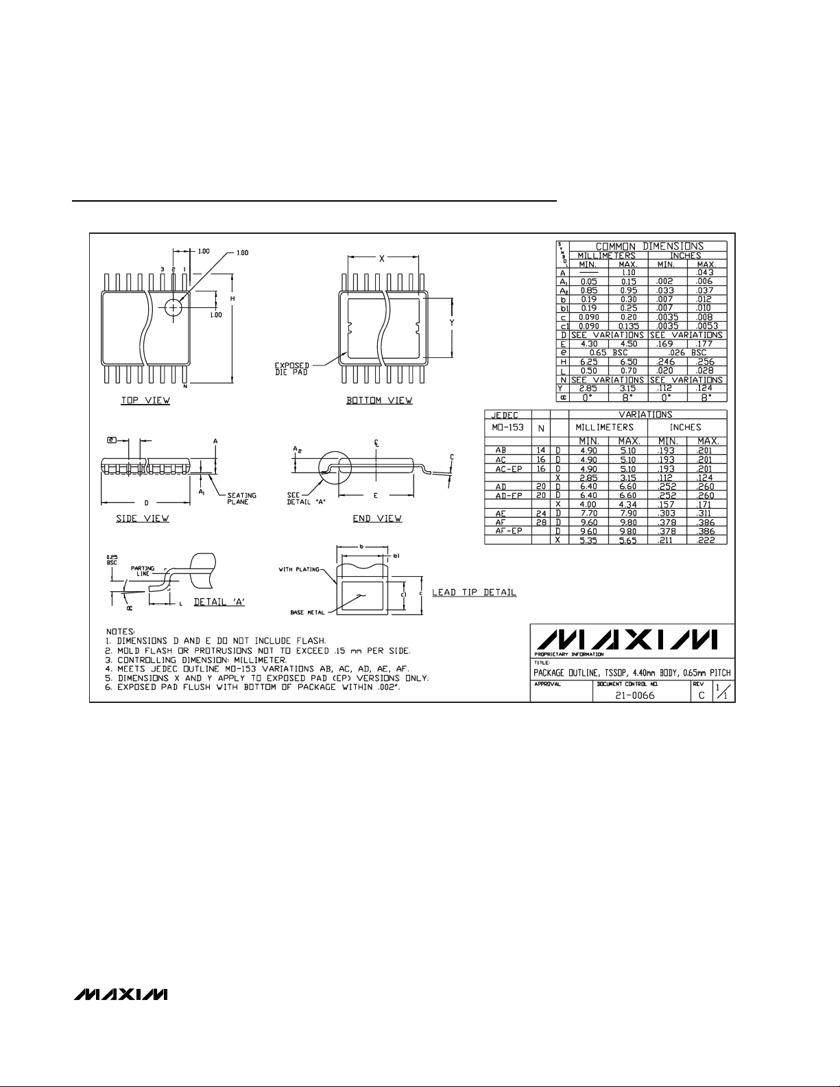
Package Information
TSSOP.EPS
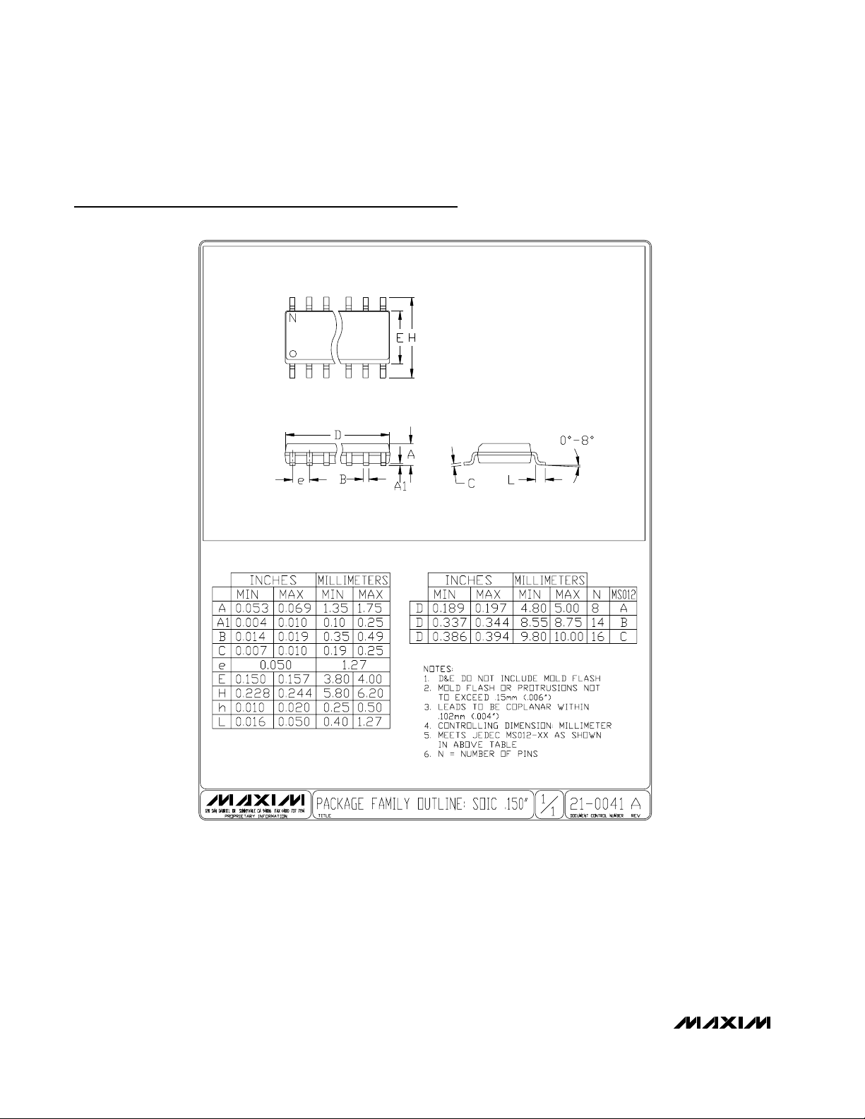
Page 14
MAX4620/MAX4630/MAX4640
±15kV ESD-Protected, Low-Voltage, Quad,
SPST, CMOS Analog Switches
14 ______________________________________________________________________________________
Package Information (continued)
SOICN.EPS
Page 15

MAX4620/MAX4630/MAX4640
±15kV ESD-Protected, Low-Voltage, Quad,
SPST, CMOS Analog Switches
______________________________________________________________________________________ 15
Package Information (continued)
PDIPN.EPS
Page 16

MAX4620/MAX4630/MAX4640
±15kV ESD-Protected, Low-Voltage, Quad,
SPST, CMOS Analog Switches
Maxim cannot assume responsibility for use of any circuitry other than circuitry entirely embodied in a Maxim product. No circuit patent licenses are
implied. Maxim reserves the right to change the circuitry and specifications without notice at any time.
16 ____________________Maxim Integrated Products, 120 San Gabriel Drive, Sunnyvale, CA 94086 408-737-7600
© 2000 Maxim Integrated Products Printed USA is a registered trademark of Maxim Integrated Products.
NOTES
 Loading...