

Page 1
General Description
The MAX4638/MAX4639 are single 8:1 and dual 4:1
CMOS analog multiplexers/demultiplexers (muxes/
demuxes). Each mux operates from a single +1.8V to
+5V supply or dual ±2.5V supplies. These devices feature 3.5Ω on-resistance (RON) when powered with a
single +5V supply and have -75dB off-isolation and
-85dB crosstalk from the output to each off channel.
The switching times are 18ns tONand 7ns t
OFF
. They
feature a -3dB 85MHz bandwidth and a guaranteed
0.25nA leakage current at +25°C.
A +1.8V to +5.5V operating range makes the MAX4638/
MAX4639 ideal for battery-powered, portable instruments. All channels guarantee break-before-make
switching. These parts feature bidirectional operation
and can handle Rail-to-Rail®analog signals. All control
inputs are TTL/CMOS-logic compatible. Decoding is in
standard BCD format, and an enable input is provided to
simplify cascading of devices. These devices are available in small 16-pin thin QFN, TSSOP, and SO packages,
as well as a 20-pin thin QFN package.
Applications
Automatic Test Equipment
Low-Voltage Data-Acquisition Systems
Audio and Video Signal Routing
Medical Equipment
Battery-Powered Equipment
Relay Replacement
Features
♦ Guaranteed R
ON
3.5Ω (+5V or ±2.5V Supplies)
6Ω (+3V Supply)
♦ Guaranteed 0.4Ω RONMatch Between Channels
♦ Guaranteed 1Ω R
ON
Flatness Over Signal Range
♦ Guaranteed Low Leakage Currents
0.25nA at +25°C
♦ Switching Times: t
ON
= 18ns, t
OFF
= 7ns
♦ +1.8V to +5.5V Single-Supply Operation
±2.5V Dual-Supply Operation
♦ Rail-to-Rail Signal Handling
♦ TTL/CMOS-Logic Compatible
♦ Crosstalk: -80dB (1MHz)
♦ Off-Isolation: -60dB (10MHz)
MAX4638/MAX4639
3.5Ω, Single 8:1 and Dual 4:1,
Low-Voltage Analog Multiplexers
________________________________________________________________ Maxim Integrated Products 1
19-1782; Rev 2; 2/04
Ordering Information
Rail-to-Rail is a registered trademark of Nippon Motorola, Ltd.
PART TEMP RANGE PIN-PACKAGE
-40°C to +85°C
16 Thin QFN (4 ✕ 4)
-40°C to +85°C 16 TSSOP
-40°C to +85°C 16 SO
-40°C to +85°C
20 Thin QFN (4 ✕ 4)
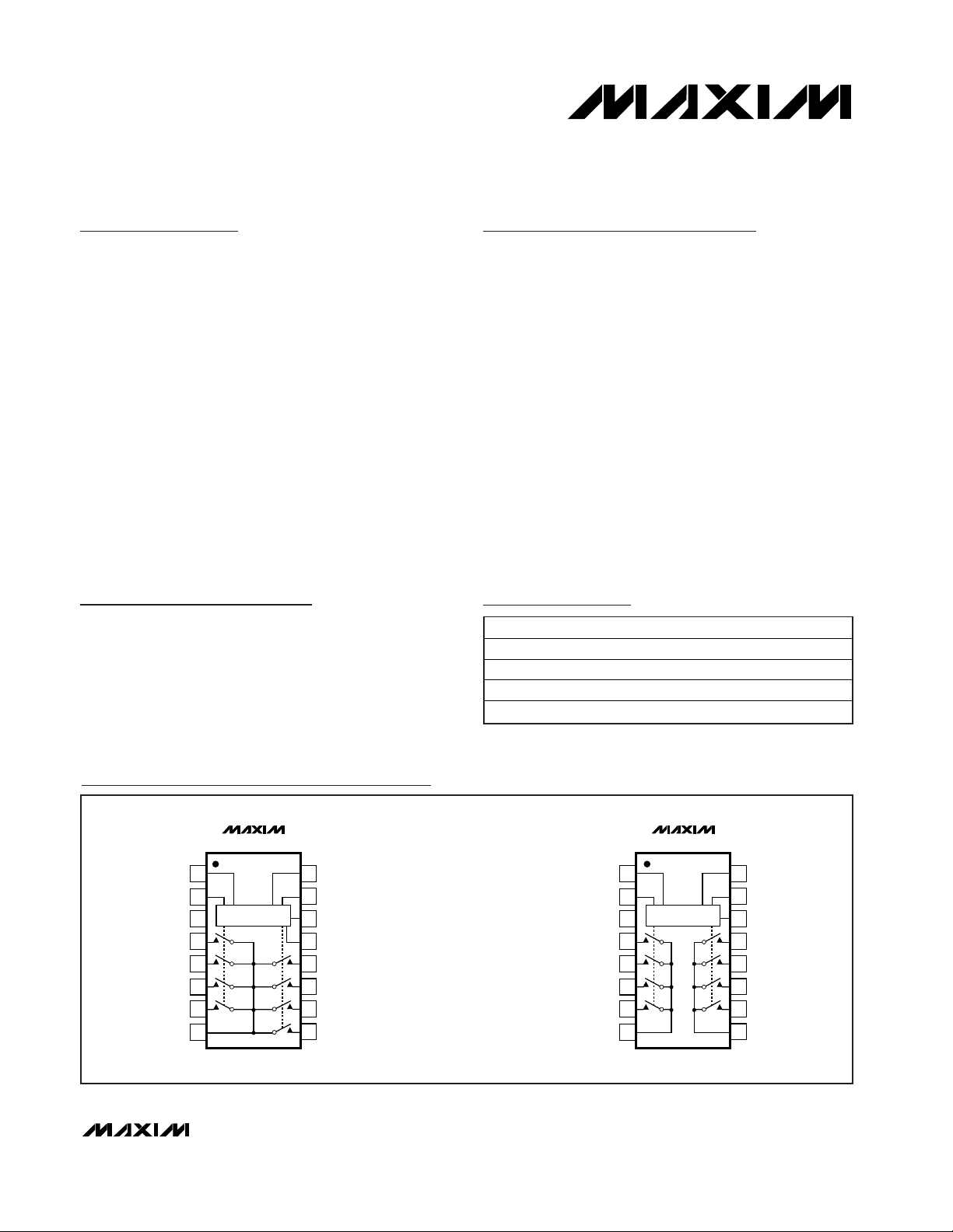
Pin Configurations/Functional Diagrams
For pricing, delivery, and ordering information, please contact Maxim/Dallas Direct! at
1-888-629-4642, or visit Maxim’s website at www.maxim-ic.com.
Ordering Information continued at end of data sheet.
MAX4638ETE
MAX4638EUE
MAX4638ESE
MAX4638ETP
TOP VIEW
MAX4638
1
A0
2
EN
LOGIC
3
V-
NO1
4
NO2
5
NO3
6
NO4
7
COM
8
TSSOP/SO
A1
16
A2
15
GND
14
V+
13
12
NO5
NO6
11
NO7
10
NO8
9
A0
EN
V-
NO1A
NO2A
NO3A
NO4A
COMA
MAX4639
1
2
3
4
5
6
7
8
TSSOP/SO
LOGIC
A1
16
GND
15
V+
14
NO1B
13
12
NO2B
NO3B
11
NO4B
10
COMB
9
Page 2
MAX4638/MAX4639
3.5Ω, Single 8:1 and Dual 4:1,
Low-Voltage Analog Multiplexers
2 _______________________________________________________________________________________
ABSOLUTE MAXIMUM RATINGS
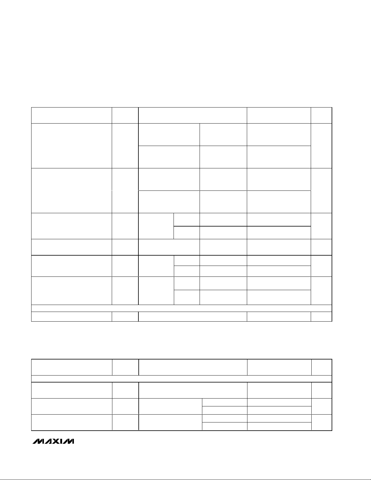
ELECTRICAL CHARACTERISTICS—+5V Single Supply
(V+ = +5V ±10%, V- = 0, VIH= +2.4V, VIL= +0.8V, TA= T
MIN
to T
MAX
, unless otherwise noted. Typical values are at TA= +25°C.) (Note 9)
Stresses beyond those listed under “Absolute Maximum Ratings” may cause permanent damage to the device. These are stress ratings only, and functional
operation of the device at these or any other conditions beyond those indicated in the operational sections of the specifications is not implied. Exposure to
absolute maximum rating conditions for extended periods may affect device reliability.
(Voltages Referenced to GND)
V+ to V- .................................................................................+6V
V+, A_, EN................................................................-0.3V to +6V
V- ............................................................................+0.3V to -6V
NO_, COM_ (Note 1) ................................... -0.3V to (V+ + 0.3V)
Continuous Current A_, EN ............................................. ±30mA
Continuous Current NO_, COM_ .................................. ±100mA
Peak Current (NO_, COM_)
(pulsed at 1ms, 10% duty cycle) .............................. ±200mA
Continuous Power Dissipation (T
A
= +70°C)
16-Pin Thin QFN (derate 16.9mW/°C above +70°C)....1349mW
16-Pin TSSOP (derate 5.7mW/°C above +70°C)............457mW
16-Pin SO (derate 8.70mW/°C above +70°C) ...............696mW
20-Pin Thin QFN (derate 16.9mW/°C above +70°C)....1349mW
Operating Temperature Range
MAX463_E_ E ................................................-40°C to +85°C
Junction Temperature......................................................+150°C
Storage Temperature Range ............................-65°C to +150°C
Lead Temperature (soldering, 10s) ................................+300°C
Note 1: Signals on COM_, NO_ exceeding V+ or V- are clamped by internal diodes. A_ and EN are clamped only to V- and can
exceed V+ up to their maximum ratings. Limit forward-diode current to maximum current rating.
PARAMETER
SYMBOL
CONDITIONS
MIN
TYP
(
MAX
UNITS
ANALOG SWITCH
Analog Signal Range
V
COM_
,
V
NO_
0V+V
TA = +25°C 2.5 3.5
On-Resistance R
ON
V
N O_
= +3.5V
4.5
Ω
TA = +25°C 0.1 0.4
On-Resistance Match
Between Channels (Notes 3, 8)
∆R
ON
V
N O_
= +3.5V
0.5
Ω
TA = +25°C
1
On-Resistance Flatness (Note 4)
)
V
N O_
= +1V , + 2V , + 3.5V
1.2
Ω
TA = +25°C
NO_ Off-Leakage Current
(Note 5)
)
V + = + 5.5V ; V
C OM _
= +1V ,
nA
TA = +25°C
COM_ Off-Leakage Current
(Note 5)
)
V + = + 5.5V ; V
C OM_
= +1V ,
nA
TA = +25°C
COM_ On-Leakage Current
(Note 5)
)
V + = + 5.5V ; V
C OM_
= +1V ,
+ 4.5V ; V
N O_
= +1V , + 4.5V ,
or fl oati ng
nA
DIGITAL I/O
Input Logic High V
IH
2.4 V
Input Logic Low V
IL
0.8 V
Input Leakage Current
I
IH
, I
IL
V
IN_
= 0 or V+
0.1 µA
Digital Input Capacitance C
IN
2pF
DYNAMIC
TA = +25°C1418
Transition Time (Note 5)
RL = 100Ω, C
L = 35p F,
V
N O1 = + 3V or 0,
20
ns
N o t e 2 )
R
FLAT(ON
I
NO_(OFF
I
COM_(OFF
I
COM_(ON
t
TRANS
V + = + 4.5V , I
V + = + 4.5V , I
V + = + 4.5V ; I
+ 4.5V ; V
N O_
+ 4.5V ; V
N O_
V
= 0 or + 3V , Fi g ur e 2
N O8
= 10m A,
C OM_
TA = T
= 10m A,
C OM_
TA = T
= 10m A;
C OM_
TA = T
= +4.5V, + 1V
T
A
= +4.5V, + 1V
T
A
TA = T
to T
MIN
MAX
to T
MIN
MAX
0.75
to T
MIN
MAX
-0.25 ±0.01 0.25
= T
MIN
to T
-0.35 0.35
MAX
-0.25 ±0.01 0.25
= T
MIN
to T
-0.75 0.75
MAX
-0.25 ±0.01 0.25
MIN
to T
-0.75 0.75
MAX
-0.1 0.005
T
= T
MIN
to T
MAX
A
Page 3
MAX4638/MAX4639
3.5Ω, Single 8:1 and Dual 4:1,
Low-Voltage Analog Multiplexers
_______________________________________________________________________________________ 3
ELECTRICAL CHARACTERISTICS—+5V Single Supply (continued)
(V+ = +5V ±10%, V- = 0, VIH= +2.4V, VIL= +0.8V, TA= T
MIN
to T
MAX
, unless otherwise noted. Typical values are at TA= +25°C.) (Note 9)
PARAMETER
SYMBOL
CONDITIONS
MIN
TYP
(
MAX
UNITS
TA = +25°C8
Break-Before-Make (Note 5) t
BBM
V
NO_
= +3V, Figure 3
1
ns
TA = +25°C1418
Enable Turn-On Time (Note 5)
)
V
NO1
= +3V, V
NO2
to
V
NO8
= 0, Figure 4
20
ns
TA = +25°C57
Enable Turn-Off Time (Note 5)
)
V
NO1
= +3V, V
NO2
to
V
NO8
= 0, Figure 4
8
ns
TA = +25°C50
On-Channel -3dB Bandwidth BW
S i g nal =
0d Bm ,
C L = 5p F,
50Ω i n and
TA = +25°C85
MHz
Charge Injection Q
C L = 1.0nF, Fig ur e 5
T
A
= +25°C13pC
NO_ Off-Capacitance
)
V
NO_
= 0V, f = 1MHz,
Figure 8
T
A
= +25°C9pF
TA = +25°C40
COM_ Off-Capacitance
f = 1MHz,
Figure 8
TA = +25°C20
pF
TA = +25°C54
Switch On-Capacitance C
(ON)
V
COM_
=
f = 1MHz,
Figure 8
TA = +25°C34
pF
C L = 5p F, R
L
= 50Ω,
f = 1M H z, V
N O_
=
1V
RM S
, Fi g ur e 6
T
A
= +25°C -55
Off-Isolation (Note 6) V
ISO
C L = 5p F, R
L
= 50Ω,
f = 10M H z, V
N O
_ =
1V
RM S
, Fi g ur e 6
T
A
= +25°C -75
dB
C L = 5p F, R
L
= 50Ω,
f = 10M H z, V
N O
_=
1V
RM S
, Fi g ur e 7
T
A
= +25°C -65
Crosstalk (Note 7) V
CT
C L = 5p F, R
L
= 50Ω,
f = 1M H z, V
N O
_ =
1V
R M S
, Fi g ur e 7
T
A
= +25°C -85
dB
Total Harmonic Distortion THD
R
L
= 600Ω,
R
FLAT(ON)/RL
TA = +25°C 0.5 %
SUPPLY
Positive Supply Current I+ V+ = +5.5V, V
IN
= 0 or V+
1.0 µA
t
ON(EN
t
OFF(EN
C
NO_(OFF
C
C OM_( OFF)
RL = 100Ω, CL = 35pF,
RL = 100Ω, CL = 35pF,
RL = 100Ω, CL = 35pF,
MAX4638
out, Fi g ur e 6
V
= + 2.5V , R
GE N
MAX4639
V
= 0V ,
C OM_
MAX4638
MAX4639
V
NO_
= 0V,
MAX4638
MAX4639
N o t e 2 )
TA = T
TA = T
TA = T
= 0,
GE N
MIN
MIN
MIN
to T
to T
to T
MAX
MAX
MAX
0.001
Page 4
MAX4638/MAX4639
3.5Ω, Single 8:1 and Dual 4:1,
Low-Voltage Analog Multiplexers
4 _______________________________________________________________________________________
ELECTRICAL CHARACTERISTICS—+3.0V Single Supply
(V+ = +2.7V to +3.3V, V- = 0, VIH= +2.0V, VIL= +0.4V, TA= T
MIN
to T
MAX
, unless otherwise noted. Typical values are at V+ = +3V
and T
A
= +25°C.) (Note 9)
PARAMETER
SYMBOL
CONDITIONS
MIN
TYP
(
)
MAX
UNITS
ANALOG SWITCH
Analog Signal Range
V
COM_
,
V
NO_
0V+V
TA = +25°C 4.5 6
On-Resistance R
ON
I
COM_
= 10mA,
V
NO_
= +1.7V
T
A
= T
MIN
to T
MAX
8
Ω
TA = +25°C
0.6
On-Resistance Match
Between Channels (Notes 3, 8)
∆R
ON
I
COM_
= 10mA,
V
NO_
= +1.7V
T
A
= T
MIN
to T
MAX
0.8
Ω
TA = +25°C12
On-Resistance Flatness (Note 4)
)
I
C OM _
= 10m A;
V
N O_
= + 1.5V , + 1.7V ,
+ 1.9V
T
A
= T
MIN
to T
MAX
2.5
Ω
TA = +25°C
NO_ Off-Leakage Current
(Note 5)
)
V+ = +3.3V;
V
COM_
= +1V, +3V;
V
NO_
= +3V, +1V
T
A
= T
MIN
to T
MAX
nA
TA = +25°C
COM_ Off-Leakage Current
(Note 5)
)
V+ = +3.3V;
V
COM_
= +1V, +3V;
V
NO_
= +3V, +1V
T
A
= T
MIN
to T
MAX
nA
TA = +25°C
COM_ On-Leakage Current
(Note 5)
)
V+ = +3.3V; V
COM_
= +1V, +3V; V
NO_
=
TA = T
MIN
to T
MAX
nA
DIGITAL I/O
Input Logic High V
IH
2.0 V
Input Logic Low V
IL
0.4 V
Input Leakage Current IIH, I
IL
V
IN_
= 0 or V+
0.1 µA
Digital Input Capacitance C
IN
2pF
DYNAMIC
TA = +25°C1620
Transition Time (Note 5)
V
NO_
= +2V, CL = 35pF,
R
L
= 100Ω, Figure 2
24
ns
TA = +25°C8
Break-Before-Make (Note 5) t
BBM
R
L
= 100Ω, Figure 3
1
ns
TA = +25°C1520
Enable Turn-On Time (Note 5)
)
V
NO_
= +2V, CL = 35pF,
R
L
= 100Ω, Figure 4
24
ns
TA = +25°C59
Enable Turn-Off Time (Note 5)
)
V
NO_
= +2V, CL = 35pF,
R
L
= 100Ω, Figure 4
10
ns
R
FLAT(ON
No te 2
0.25
I
NO_(OFF
I
COM_(OFF
I
COM_(ON
t
TRANS
t
ON(EN
t
OFF(EN
+1V, +3V, or floating
V
= +2V, CL = 35pF,
NO_
TA = T
TA = T
TA = T
TA = T
-0.25 ±0.01 0.25
-0.35 0.35
-0.25 ±0.01 0.25
-0.35 0.35
-0.25 ±0.01 0.25
-0.35 0.35
-0.1 0.005
to T
MIN
MAX
to T
MIN
MAX
to T
MIN
MAX
to T
MIN
MAX
Page 5
MAX4638/MAX4639
3.5Ω, Single 8:1 and Dual 4:1,
Low-Voltage Analog Multiplexers
_______________________________________________________________________________________ 5
ELECTRICAL CHARACTERISTICS—+3.0V Single Supply (continued)
(V+ = +2.7V to +3.3V, V- = 0, VIH= +2.0V, VIL= +0.4V, TA= T
MIN
to T
MAX
, unless otherwise noted. Typical values are at V+ = +3V
and T
A
= +25°C.) (Note 9)
PARAMETER
SYMBOL
CONDITIONS
MIN
TYP
(
)
MAX
UNITS
CL = 5pF, R
L
= 50Ω,
f = 10MHz,
TA = +25°C55
Off-Isolation (Note 6) V
ISO
CL = 5pF, R
L
= 50Ω,
f = 1M Hz, V
N O_
= 1V
RM S
,
Figure 6
TA = +25°C -75
dB
C L = 5p F, R
L
= 50Ω,
f = 10MH z, V
N O_
= 1V
RM S
,
Figure 7
TA = +25°C -65
Crosstalk (Note 7) V
CT
C L = 5p F, R
L
= 50Ω,
f = 1MH z, V
NO_
= 1V
RMS
,
Fig ur e 7
T
A
= +25°C -85
dB
TA = +25°C50
On-Channel -3dB Bandwidth BW
Signal =
and out,
Figure 6
TA = +25°C85
MHz
NO_ Off-Capacitance
)
V
NO_
= 0V, f = 1MHz,
Figure 8
T
A
= +25°C9pF
TA = +25°C40
COM_ Off-Capacitance
)
f = 1MHz,
Figure 8
TA = +25°C20
pF
TA = +25°C54
Switch On-Capacitance C
(ON)
= 0V,
f = 1MHz,
Figure 8
TA = +25°C34
pF
SUPPLY
Positive Supply Current I+ V+ = +3.3V, V
IN_
= 0 or V+
1µA
ELECTRICAL CHARACTERISTICS—±2.5V Dual Supplies
(V+ = +2.5 ±10%, V- = -2.5V ±10%, VIH= +2.0V, VIL= +0.4V, TA=T
MIN
to T
MAX
, unless otherwise noted. Typical values are at
V± = ±2.5V and T
A
= +25°C.)
PARAMETER
SYMBOL
CONDITIONS
MIN
TYP
(
MAX
UNITS
ANALOG SWITCH
Analog Signal Range
V
COM_
,
V
NO_
V- V+ V
TA = +25°C 2.5 3.5
On-Resistance R
ON
V + = + 2.25V, V - = -2.25V
4.5
Ω
TA = +25°C 0.2 0.4
On-Resistance Match
Between Channels (Notes 3, 8)
∆R
ON
V + = + 2.25V , V - = - 2.25V
0.5
Ω
C
NO_(OFF
C
C OM _( OFF
V
= + 1V
N O_
0dBm, 50Ω in
V
= 0V ,
C OM _
V
= V
COM
I
= 10m A, V
COM_
I
= 10m A, V
COM_
RM S
, Fi g ur e 6
MAX4638
MAX4639
MAX4638
MAX4639
NO_
MAX4638
MAX4639
= ±1.5V,
NO_
= ±1.5V,
NO_
TA = T
TA = T
to T
MIN
MAX
to T
MIN
MAX
No te 2
0.001
N o t e 2 )
Page 6

MAX4638/MAX4639
3.5Ω, Single 8:1 and Dual 4:1,
Low-Voltage Analog Multiplexers
PARAMETER
SYMBOL
CONDITIONS
MIN
TYP
(
MAX
UNITS
TA = +25°C
1
On-Resistance Flatness
(Note 4)
)
1.2
Ω
TA = +25°C
NO_ Off-Leakage
Current (Note 5)
)
V + = + 2.75V; V - = -2.75V ;
V
COM_
= +1V, +2.5V;
V
NO_
= +2.5V, +1V
nA
TA = +25°C
COM_ Off-Leakage
Current (Note 5)
)
V + = + 2.75V; V - = -2.75;
V
C OM_
= +1V , + 2.5V ;
V
N O_
= +2.5V, + 1V
nA
TA = +25°C
COM_ On-Leakage
Current (Note 5)
)
V + = + 2.5V ; V - = - 2.5;
V
C OM _
= + 1V , + 2.5V ;
V
NO_
= + 1V , + 2.5V , or
fl oati ng
nA
DIGITAL I/O
Input Logic High V
IH
2.0 V
Input Logic Low V
IL
0.4 V
Input Leakage Current IIH, IILV
IN_
= 0 or V+
0.1 µA
Digital Input Capacitance C
IN
2pF
DYNAMIC
TA = +25°C 16 20
Transition Time (Note 5)
R
L
= 100Ω, Figure 2
24
ns
TA = +25°C 14 18
Enable Turn-On Time
(Note 5)
)
R
L
= 100Ω, Figure 4
20
ns
TA = +25°C 5 7
Enable Turn-Off Time
(Note 5)
)
V
N O_
= +1.2V, C L = 35p F,
R
L
= 100Ω, Figure 4
8
ns
TA = +25°C 8
Break-Before-Make (Note 5) t
BBM
R
L
= 100Ω, Figure 3
1
ns
ELECTRICAL CHARACTERISTICS—±2.5V Dual Supplies (continued)
(V+ = +2.5 ±10%, V- = -2.5V ±10%, VIH= +2.0V, VIL= +0.4V, TA= T
MIN
to T
MAX
, unless otherwise noted. Typical values are at
V± = ±2.5V and T
A
= +25°C.)
Note 2: The algebraic convention, where the most negative value is a minimum and the most positive value a maximum, is used in
this data sheet.
Note 3: ∆R
ON
= R
ON(MAX)
- R
ON(MIN)
.
Note 4: Flatness is defined as the difference between the maximum and minimum value of on-resistance as measured over the
specified analog signal ranges.
Note 5: Guaranteed by design.
Note 6: Off-Isolation = 20log
10(VCOM_
/ V
NO_
), V
COM_
= output, V
NO_
= input to off switch.
Note 7: Between any two switches.
Note 8: ∆R
ON
matching specifications for thin QFN packaged parts are guaranteed by design.
Note 9: Parts are tested at +85°C and guaranteed by design over the entire temperature range.
6 ______________________________________________________________________________________
R
FLAT(ON
I
NO_ (OFF
I
COM_ (OFF
I
COM_ (ON
I
= 10m A; V
C OM_
N O_
0; V + = + 2.25V ; V - = - 2.25V
= ±1.5V ,
= T
MIN
MIN
MIN
MIN
to T
to T
to T
to T
T
A
TA = T
TA = T
TA = T
MAX
-0.25 ±0.01 0.25
-0.35 0.35
MAX
-0.25 ±0.01 0.25
-0.35 0.35
MAX
-0.25 ±0.01 0.25
-0.35 0.35
MAX
N o t e 2 )
0.75
V
= +1.2V, CL = 35pF,
t
TRANS
NO_
t
ON(EN
V
= + 1.2V , C L = 35p F,
N O_
t
OFF(EN
V
= + 1.2V , C L = 35p F,
N O_
-0.1 0.005
TA = T
TA = T
TA = T
MIN
MIN
MIN
to T
to T
to T
MAX
MAX
MAX
TA = T
MIN
to T
MAX
Page 7

MAX4638/MAX4639
3.5Ω, Single 8:1 and Dual 4:1,
Low-Voltage Analog Multiplexers
_______________________________________________________________________________________ 7
0
5
10
15
20
25
02.02.51.0 1.50.5 3.0 3.5 4.0 4.5 5.0
ON-RESISTANCE vs. V
COM
MAX4638 toc01
V
COM
(V)
R
ON
(Ω)
V+ = +1.8V
V+ = +3V
V+ = +5V
0
1.0
0.5
1.5
3.0
3.5
2.5
2.0
4.0
01.01.5 2.0 2.50.5 3.0 3.5 4.0 4.5 5.0
ON-RESISTANCE vs. V
COM
AND
TEMPERATURE
MAX4638 toc02
V
COM
(V)
R
0N
(Ω)
TA = +85°C
TA = -40°C
TA = +25°C
V+ = +5V
0
2
1
4
3
5
6
01.01.50.5 2.0 2.5 3.0
ON-RESISTANCE vs. V
COM
AND
TEMPERATURE
MAX4638 toc03
V
COM
(V)
R
ON
(Ω)
TA = +85°C
TA = -40°C
TA = +25°C
V+ = +3V
60
100
80
140
120
180
160
200
1.0 3.02.0 4.0 5.01.5 3.52.5 4.5 5.5 6.0
SUPPLY CURRENT
vs. SUPPLY VOLTAGE
MAX4638 toc04
SUPPLY VOLTAGE (V)
SUPPLY CURRENT (pA)
0
6
4
2
8
10
12
14
16
18
20
-2.5 -0.5 1.5 3.5
CHARGE INJECTION vs. V
COM
MAX4638 toc05
V
COM
(V)
CHARGE (pC)
V+ = +5V
V± = ±2.5V
5.5
10
1
0.1
0.01
0.001
-40 10-15 35 6085
SUPPLY CURRENT
vs. TEMPERATURE
MAX4638 toc06
TEMPERATURE (°C)
SUPPLY CURRENT (nA)
0.6
0.8
1.0
1.2
1.4
1.6
1.8
1.8 2.82.3 3.3 3.8 4.3 4.8 5.3
LOGIC LEVEL THRESHOLD vs.
SUPPLY VOLTAGE AND TEMPERATURE
MAX4638 toc07
SUPPLY VOLTAGE (V)
LOGIC VOLTAGE (V)
TA = +85°C
TA = +25°C
TA = -40°C
0
10
5
25
20
15
40
35
30
45
1.5 3.0 3.52.0 2.5 4.0 4.5 5.0 5.5
ENABLE TURN-ON/TURN-OFF TIME
vs. SUPPLY VOLTAGE
MAX4638 toc08
SUPPLY VOLTAGE (V)
TIME (ns)
t
ON
t
OFF
0
2
4
6
8
10
12
14
16
-40 -15 10 35 60 85
ENABLE TURN-ON/TURN-OFF TIME
vs. TEMPERATURE
MAX4638 toc09
TEMPERATURE (°C)
TIME (ns)
t
ON
t
OFF
Typical Operating Characteristics
(V+ = +5V, V- = 0, TA= +25°C, unless otherwise noted.)
Page 8

MAX4638/MAX4639
3.5Ω, Single 8:1 and Dual 4:1,
Low-Voltage Analog Multiplexers
-120
-80
-100
-40
-60
0
-20
0.01 10.1 10 100 1000
FREQUENCY RESPONSE
MAX4638 toc10
FREQUENCY (MHz)
RESPONSE (dB)
ON-RESPONSE MAX4638
ON-RESPONSE MAX4639
OFF-ISOLATION
CROSSTALK
0.01
0.001
1
0.1
100
10
1000
-40 0-20 20 40 8060
ON/OFF-LEAKAGE CURRENT
vs. TEMPERATURE
MAX4638 toc11
TEMPERATURE (°C)
LEAKAGE CURRENT (pA)
OFF-LEAKAGE
ON-LEAKAGE
0
0.02
0.06
0.04
0.08
0.10
TOTAL HARMONIC DISTORTION
vs. FREQUENCY
MAX4638 toc12
FREQUENCY (kHz)
THD (%)
0.01 10.1 10 100
V+ = +2.5V
V- = -2.5V
5Vp-p SIGNAL
600Ω IN AND OUT
Pin Description
PIN
MAX4638 MAX4639
THIN QFN THIN QFN
DIP/SO
16-PIN 20-PIN
DIP/SO
NAME FUNCTION
1, 15, 16
———A0, A2, A1 Address Inputs
———1, 16 15, 14 19, 17 A0, A1 Address Inputs
21612161 EN Enable
3123 12 V- Negative-Supply Voltage Input
4–7 2–5 3–6 — — — NO1–N04 Bidirectional Analog Inputs
———4–7 2–5 3–6
Bidirectional Analog Inputs
867——— COM Bidirectional Analog outputs
———8, 9 6, 7 7, 9
Bidirectional Analog outputs
9–12 7–10 10–13 — — — NO8–NO5 Bidirectional Analog Inputs
———10–13 8–11 10–13
Bidirectional Analog Inputs
13 11 14 14 12 14 V+ Positive-Supply Voltage Input
14 12 15 15 13 15 GND Ground
——
8, 9,
16, 20
——
8, 16,
18, 20
N.C.
No Connection. Not internally
connected.
—EPEP— EP EP PAD Exposed Pad. Connect to V-.
8 _______________________________________________________________________________________
Typical Operating Characteristics (continued)
(V+ = +5V, V- = 0, TA= +25°C, unless otherwise noted.)
16-PIN 20-PIN
15, 14, 13 19, 18, 17
NO1A–NO4A
COMA, COMB
NO4B–NO1B
Page 9

MAX4638/MAX4639
3.5Ω, Single 8:1 and Dual 4:1,
Low-Voltage Analog Multiplexers
_______________________________________________________________________________________ 9
Detailed Description
The MAX4638/MAX4639 are low-voltage, CMOS analog
muxes. The MAX4638 is an 8:1 mux that switches one
of eight inputs (NO1–NO8) to a common output (COM)
as determined by the 3-bit binary inputs A0, A1, and
A2. The MAX4639 is a 4:1 dual mux that switches one
of four differential inputs to a common differential output as determined by the 2-bit binary inputs A0 and A1.
Both the MAX4638/MAX4639 have an EN input that can
be used to enable or disable the device. When disabled, all channels are switched off. See Truth Tables.
Applications Information
Overvoltage Protection
Proper power-supply sequencing is recommended for
all CMOS devices. Do not exceed the absolute maximum ratings because stresses beyond the listed ratings can cause permanent damage to the devices.
Always sequence V+ on first, then V-, followed by the
logic inputs. If power-supply sequencing is not possible, add two small-signal diodes (D1, D2) in series with
the supply pins for overvoltage protection (Figure 1).
Adding diodes reduces the analog signal range to one
diode drop below V+ and one diode drop above V-, but
does not affect the devices’ low switch resistance.
Device operation is unchanged, and the difference
between V+ and V- should not exceed 6V. These protection diodes are not recommended when using a single supply. For single-supply operation, V- should be
connected to GND as close to the device as possible.
COM_
V-
V+
NO_
* INTERNAL PROTECTION DIODES
D2
D1
-2.5V
+2.5V
MAX4638
MAX4639
*
*
*
*
Figure 1. Overvoltage Protection Using External Blocking
Diodes
A2 A1 A0 EN ON SWITCH
XX X0 None
00 0 1 NO1
00 1 1 NO2
01 0 1 NO3
01 1 1 NO4
10 0 1 NO5
10 1 1 NO6
11 0 1 NO7
11 1 1 NO8
MAX4638 (Single 8-to-1 Mux) MAX4639 (Dual 4-to-1 Mux)
Truth Tables
Ordering Information (continued)
PART TEMP RANGE PIN-PACKAGE
-40°C to +85°C
16 Thin QFN (4 ✕ 4)
-40°C to +85°C 16 TSSOP
-40°C to +85°C 16 SO
-40°C to +85°C
20 Thin QFN (4 ✕ 4)
MAX4639ETE
MAX4639EUE
MAX4639ESE
MAX4639ETP
A1 A0 EN COMA COMB
XX 0None None
00 1NO1A NO1B
01 1NO2A NO2B
10 1NO3A NO3B
11 1NO4A NO4B
Page 10

MAX4638/MAX4639
3.5Ω, Single 8:1 and Dual 4:1,
Low-Voltage Analog Multiplexers
10 ______________________________________________________________________________________
Test Circuits/Timing Diagrams
50%
t
R
< 5ns
t
F
< 5ns
+3V
0V
V
N01
ADDRESS
INPUT
V
IN
SWITCH
OUTPUT
V
OUT
V+
V
OUT
V-
GND
V+
A1
V-
A0
A2
EN
NO1
NO2–NO7
NO8
COM
V
NO1
V
NO8
50Ω
MAX4638
100Ω
35pF
90%
10%
t
TRANS
V+
V
OUT
V-
GND
V+
A1
V-
A0
EN
NO1B
V
NO8
NO1A–NO4A
COMB
V
NO1
50Ω
MAX4639
100Ω
35pF
V
IH
V
IH
V
IN
V
IN
NO4B
t
TRANS
V
N08
Figure 2. Transition Time
50%
t
BBM
tR < 5ns
t
F
< 5ns
V
N0_
+3V
0V
ADDRESS
INPUT
V
A
SWITCH
OUTPUT
V
OUT
V+
V-
GND
V+
A0
V-
A1
A2
EN
50Ω
MAX4638
90%
0V
V
A
V
IH
V
NO1
NO1
NO8
V
NO8
COM
V
OUT
NO2–NO7
100Ω
35pF
Figure 3. MAX4638 Break-Before-Make Interval
Page 11

MAX4638/MAX4639
3.5Ω, Single 8:1 and Dual 4:1,
Low-Voltage Analog Multiplexers
______________________________________________________________________________________ 11
50%
90%
t
R
< 5ns
t
F
< 5ns
V
OUT
+3V
0V
V
NO1
0V
LOGIC
INPUT
V
EN
SWITCH
OUTPUT
V+
V-
GND
V+
A1
V-
A0
A2
EN
NO1
NO2–NO8
COM
50Ω
MAX4638
100Ω
35pF
V+
V
OUT
V-
GND
V+
V-
NO1B
NO_, COMA
COMB
V
NO1
V
EN
MAX4639
100Ω
35pF
t
OFF(EN)
90%
V
OUT
V
NO1
A0
A1
EN
50Ω
V
EN
t
ON(EN)
Figure 4. Enable Switching Time
Figure 5. Charge Injection
∆V
OUT
+3V
0V
LOGIC
INPUT
V
EN
V+
V
OUT
V-
GND
V+
A1
V-
A0
A2
EN
COM
MAX4638
MAX4639
C
L
1nF
V
OUT
NO_
CHANNEL
SELECT
R
S
V
S
OFF OFFOFF ON ON ON
∆V
OUT
IS THE MEASURED VOLTAGE DUE TO CHARGE TRANSFER
ERROR Q WHEN THE CHANNEL TURNS OFF.
Q = ∆V
OUT
✕ C
L
V
EN
Test Circuits/Timing Diagrams (continued)
Page 12

MAX4638/MAX4639
3.5Ω, Single 8:1 and Dual 4:1,
Low-Voltage Analog Multiplexers
12 ______________________________________________________________________________________
V+
V
OUT
V-
GND
V+
A1
V-
A0
A2
NO8
COM
MAX4638
MAX4639
NO1
R
S
= 50Ω
V
IN
EN
1µF
R
L
50Ω
C
L
5pF
OFF-ISOLATION = 20log
V
OUT
V
IN
V
EN
Figure 7. Crosstalk
V+
V
OUT
V-
GND
V+
A1
V-
A0
A2
NO8
COM
MAX4638
MAX4639
NO2
R
G
= 50Ω
V
IN
EN
1µF
R
L
50Ω
C
L
5pF
NO1
R
50Ω
CROSSTALK = 20log
V
OUT
V
IN
V
EN
1µF
Figure 8. Channel Off/On-Capacitance
V+
V-
GND
V+
A2
V-
A1
A0
NO8
MAX4638
MAX4639
CHANNEL
SELECT
NO1
COM
EN
1MHz
CAPACITANCE
ANALYZER
f = 1MHz
V
EN
Test Circuits/Timing Diagrams (continued)
Chip Information
TRANSISTOR COUNT: 632
Figure 6. Off-Isolation/On-Channel Bandwidth
Note: Exposed pad on thin QFN packages is connected to V-.
Page 13

MAX4638/MAX4639
3.5Ω, Single 8:1 and Dual 4:1,
Low-Voltage Analog Multiplexers
______________________________________________________________________________________ 13
16
15
14
13
EN
A0
A1
A2
9
10
11
12
NO6
NO5
V+
GND
4
3
2
1
NO3
NO2
NO1
V-
5
6
7
8
NO4
COM
NO8
NO7
MAX4638
16
15
14
13
EN
A0
A1
GND
9
10
11
12
NO3B
NO2B
NO1B
V+
4
3
2
1
NO3A
NO2A
NO1A
V-
5
6
7
8
NO4A
COMA
COMB
NO4B
MAX4639
TOP VIEW
20
19
18
17
N.C.
A0
A1
A2
16 N.C.
13
12
11
14
15
NO6
NO5
V+
GND
NO7
4
3
2
1
NO2
NO1
V-
EN
5NO3
6
7
8
9
NO4
COM
N.C.
N.C.
10NO8
MAX4638
THIN QFN
20
19
18
17
N.C.A0N.C.
A1
16 N.C.
13
12
11
14
15
NO2B
NO1B
V+
GND
NO3B
4
3
2
1
NO2A
NO1A
V-
EN
5NO3A
6
7
8
9
NO4A
COMA
N.C.
COMB
10NO4B
MAX4639
THIN QFN
THIN QFN THIN QFN
Pin Configurations (continued)
Page 14

MAX4638/MAX4639
3.5Ω, Single 8:1 and Dual 4:1,
Low-Voltage Analog Multiplexers
14 ______________________________________________________________________________________
TSSOP4.40mm.EPS
Package Information
(The package drawing(s) in this data sheet may not reflect the most current specifications. For the latest package outline information,
go to www.maxim-ic.com/packages.)
Page 15

MAX4638/MAX4639
3.5Ω, Single 8:1 and Dual 4:1,
Low-Voltage Analog Multiplexers
______________________________________________________________________________________ 15
Package Information (continued)
(The package drawing(s) in this data sheet may not reflect the most current specifications. For the latest package outline information,
go to www.maxim-ic.com/packages.)
24L QFN THIN.EPS
C
1
2
21-0139
PACKAGE OUTLINE
12, 16, 20, 24L THIN QFN, 4x4x0.8mm
C
2
2
21-0139
PACKAGE OUTLINE
12, 16, 20, 24L THIN QFN, 4x4x0.8mm
Page 16

MAX4638/MAX4639
3.5Ω, Single 8:1 and Dual 4:1,
Low-Voltage Analog Multiplexers
SOICN .EPS
PACKAGE OUTLINE, .150" SOIC
1
1
21-0041
B
REV.DOCUMENT CONTROL NO.APPROVAL
PROPRIETARY INFORMATION
TITLE:
TOP VIEW
FRONT VIEW
MAX
0.010
0.069
0.019
0.157
0.010
INCHES
0.150
0.007
E
C
DIM
0.014
0.004
B
A1
MIN
0.053A
0.19
3.80 4.00
0.25
MILLIMETERS
0.10
0.35
1.35
MIN
0.49
0.25
MAX
1.75
0.050
0.016L
0.40 1.27
0.3940.386D
D
MINDIM
D
INCHES
MAX
9.80 10.00
MILLIMETERS
MIN
MAX
16 AC
0.337 0.344 AB8.758.55 14
0.189 0.197 AA5.004.80 8
N MS012
N
SIDE VIEW
H 0.2440.228 5.80 6.20
e 0.050 BSC 1.27 BSC
C
HE
e
B
A1
A
D
0∞-8∞
L
1
VARIATIONS:
Maxim cannot assume responsibility for use of any circuitry other than circuitry entirely embodied in a Maxim product. No circuit patent licenses are
implied. Maxim reserves the right to change the circuitry and specifications without notice at any time.
Maxim Integrated Products, 120 San Gabriel Drive, Sunnyvale, CA 94086 408-737-7600 _____________________16
© 2004 Maxim Integrated Products Printed USA is a registered trademark of Maxim Integrated Products.
Package Information (continued)
(The package drawing(s) in this data sheet may not reflect the most current specifications. For the latest package outline information,
go to www.maxim-ic.com/packages.)
 Loading...