

Page 1
General Description
The MAX4635/MAX4636 are fast, dual 4Ω singlepole/double-throw (SPDT) analog switches that operate
with supply voltages from +1.8V to +5.5V. High switching speeds, 1Ω on-resistance flatness, and low power
consumption make these devices ideal for audio/video,
communications, and battery-operated devices.
Containing two independently controllable SPDT
switches in 10-pin µMAX and 10-pin 3mm x 3mm thin
QFN packages, the MAX4635/MAX4636 use little board
space, and have low power consumption ensuring minimal impact on your power budget. The analog signal
range extends to the supply rails. The MAX4635 has
inverted logic compared to the MAX4636.
________________________Applications
Battery-Powered Equipment
Relay Replacement
Audio and Video Signal Routing
Low-Voltage Data-Acquisition Systems
Sample-and-Hold Circuits
Communications Circuits
Features
♦ Guaranteed On-Resistance
4Ω (max) +5V Supply
5.5Ω (max) +3V Supply
♦ Guaranteed Match Between Channels
0.2Ω (max)
♦ Guaranteed Flatness Over Signal Range
1Ω (max) with +5V Supply
♦ Fast Switching Speeds
14ns (max) Turn-On Time
6ns (max) Turn-Off Time
♦ 1.8V Operation
100Ω (typ) On-Resistance Over Temperature
56ns (typ) Turn-On Time
17ns (typ) Turn-Off Time
♦ +1.8V to +5.5V Single-Supply Operation
♦ Rail-to-Rail
®
Signal Handling
♦ Low Crosstalk: -67dB at 1MHz
♦ High Off-Isolation: -65dB at 1MHz
♦ THD: 0.1%
MAX4635/MAX4636
Fast, Low-Voltage, Dual 4Ω SPDT
CMOS Analog Switches
________________________________________________________________ Maxim Integrated Products 1
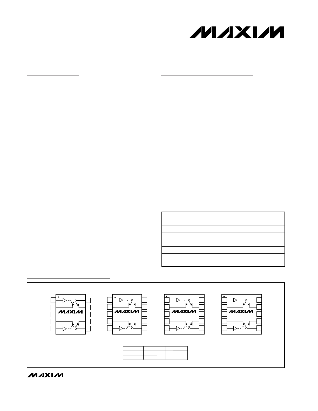
Pin Configuration/Functional Diagram/Truth Table
19-1709; Rev 2; 5/03
Ordering Information
Rail-to-Rail is a registered trademark of Nippon Motorola, Ltd.
For pricing, delivery, and ordering information, please contact Maxim/Dallas Direct! at
1-888-629-4642, or visit Maxim’s website at www.maxim-ic.com.
PART TEMP RANGE
MAX4635EUB -40°C to +85°C 10 µMAX —
MAX4635ETB -40°C to +85°C 10 Thin
MAX4636EUB -40°C to +85°C 10 µMAX —
MAX4636ETB -40°C to +85°C 10 Thin
PIN-
PACKAGE
QFN (3
✕ 3)
✕ 3)
QFN (3
TOP
MARK
AAT
AAO
TOP VIEW
1
IN1
NO1
GND
1
2
3
MAX4635
4
5
µMAX
10
IN1
COM1
2
NC1
9
NC1
3
GND
8
V+
7
NC2NO2
COM2IN2
6
MAX4636
4
5
µMAX
SWITCHES SHOWN FOR "0" INPUT
10
COM1
9
NO1
8
V+
7
NO2NC2
COM2IN2
6
NO_ TO COM_ NC_ TO COM_
IN_
0
1
OFF
ON
1
IN1
2
NO1
3
GND
4
5
3 x 3 THIN QFN
MAX4635
ON
OFF
1
10
IN1
COM1
2
NC1
9
NC1
3
GND
8
V+
7
NC2NO2
COM2IN2
6
MAX4636
4
5
3 x 3 THIN QFN
10
9
8
7
6
COM1
NO1
V+
NO2NC2
COM2IN2
Page 2
MAX4635/MAX4636
Fast, Low-Voltage, Dual 4Ω SPDT
CMOS Analog Switches
2 _______________________________________________________________________________________
ABSOLUTE MAXIMUM RATINGS
ELECTRICAL CHARACTERISTICS—Single +5V Supply
(V+ = +4.5V to +5.5V, VIH= +2.4V, V
IL
= +0.8V, TA= T
MIN
to T
MAX
, unless otherwise noted. Typical values are at TA= +25°C.)
(Notes 2, 9)
Stresses beyond those listed under “Absolute Maximum Ratings” may cause permanent damage to the device. These are stress ratings only, and functional
operation of the device at these or any other conditions beyond those indicated in the operational sections of the specifications is not implied. Exposure to
absolute maximum rating conditions for extended periods may affect device reliability.
(Voltages Referenced to GND)
V+, IN_ .....................................................................-0.3V to +6V
COM_, NC_, NO_ (Note 1) .......................... -0.3V to (V+ + 0.3V)
Continuous Current into Any Terminal .............................±30mA
Peak Current into COM_, NC_, NO_
(pulsed at 1ms, 10% duty cycle).................................±100mA
Continuous Power Dissipation (T
A
= +70°C)
10-Pin µMAX (derate 4.7mW/°C above +70°C) ............330mW
10-Pin Thin QFN (derate 24.4mW/°C above +70°C) ..1951mW
Operating Temperature Range .......................... -40°C to +85°C
Storage Temperature Range ........................... -65°C to +150°C
Lead Temperature (soldering, 10s) ............................... +300°C
Note 1: Signals on NO_, NC_, or COM_ exceeding V+ or GND are clamped by internal diodes. Limit forward-diode current to maxi-
mum current rating.
)
)
)
)
)
PARAMETER SYMBOL CONDITIONS MIN TYP MAX UNITS
ANALOG SWITCH
Analog Signal Range
On-Resistance R
On-Resistance Match
Between Channels (Notes 3, 4)
On-Resistance Flatness
(Note 5)
NO_, NC_ Off-Leakage Current
(Note 6)
COM_ Off-Leakage Current
(Note 6)
COM_ On-Leakage Current
(Note 6)
DIGITAL I/O (IN1, IN2)
Input Logic High V
Input Logic Low V
Input Leakage Current IIH, I
V
,
COM_
,
V
NO_
V
NC_
ON
∆R
ON
R
FLAT(ON
I
NC_(OFF
I
NO_(OFF
I
COM_(OFF
I
COM_(ON
IH
IL
IL
V + = 4.5V , I
V
NO_
V + = 4.5V , I
V
NO_
V+ = 4.5V, I
V
NO_
V+ = 5.5V; V
,
4.5V ; V
or V
or V
or V
N O_
C OM_
NC_
C OM_
NC_
COM_
NC_
COM_
or V
= 0 to V+
= 0 to V+
= 0 to V+
N C _
1V
V+ = 5.5V; V
4.5V; V
N O_
COM_
or V
1V
V + = 5.5V ; V
1V ; V
N O_
or V
C OM_
N C _
1V or floating
V
= 0 or +5.5V -100 5 100 nA
IN_
= 10m A,
= 10m A,
= 10mA,
= 1V,
TA = +25°C 2.5 4
T
= T
MIN
to T
MAX
A
TA = +25°C 0.1 0.2
T
= T
MIN
to T
MAX
A
TA = +25°C 0.5 1
T
= T
MIN
to T
MAX
A
TA = +25°C-0.1±0.01 0.1
= 4.5V ,
= T
N C _
= 4.5V,
= 1V,
= 4.5V ,
T
A
TA = +25°C-0.1±0.01 0.1
T
A
TA = +25°C-0.1±0.01 0.1
= T
MIN
MIN
to T
to T
MAX
MAX
= 4.5V ,
= T
MIN
to T
MAX
T
A
0V+V
4.5
0.4
1.2
-0.3 0.3
-0.3 0.3
-0.3 0.3
2.4 V
0.8 V
Ω
Ω
Ω
nA
nA
nA
Page 3
MAX4635/MAX4636
Fast, Low-Voltage, Dual 4Ω SPDT
CMOS Analog Switches
_______________________________________________________________________________________ 3
ELECTRICAL CHARACTERISTICS—Single +5V Supply (continued)
(V+ = +4.5V to +5.5V, VIH= +2.4V, V
IL
= +0.8V, TA= T
MIN
to T
MAX
, unless otherwise noted. Typical values are at TA= +25°C.)
(Notes 2, 9)
ELECTRICAL CHARACTERISTICS—Single +3V Supply
(V+ = +2.7V to +3.6V, VIH= +2.0V, VIL= +0.8V, TA = T
MIN
to T
MAX
, unless otherwise noted. Typical values are at TA= +25°C.)
(Notes 2, 9)
)
)
)
)
),
)
)
PARAMETER SYMBOL CONDITIONS MIN TYP MAX UNITS
DYNAMIC
Turn-On Time
(Note 6)
Turn-Off Time
(Note 6)
Break-Before-Make Time
(Note 6)
Charge Injection Q V
NO_, NC_ Off-Capacitance
COM_ On-Capacitance C
Off-Isolation (Note 7) V
Crosstalk (Note 8) V
Total Harmonic Distortion THD RL = 600Ω, V
SUPPLY
Positive Supply Current I+ V+ = 5.5V, V
t
ON
t
OFF
t
BBM
C
NO_(OFF
C
NC_(OFF
COM_(ON
ISO
CT
V
, V
NO_
NC_
= 300Ω, CL = 35pF,
R
L
Figure 1a
V
, V
NO_
NC_
= 300Ω, CL = 35pF,
R
L
Figure 1a
V
, V
NO_
NC_
R
= 300Ω, CL = 35pF,
L
Figure 1b
= 2V, R
GEN
,
V
, V
NO_
V
COM_
= GND, f = 1MHz, Figure 3 9 pF
NC_
= GND, f = 1MHz, Figure 3 32 pF
CL = 5pF, R
C L = 5p F, R
L
CL = 5pF, R
CL = 5pF, R
= 3V;
= 3V;
= 3V;
= 0, CL = 1.0nF, Figure 2 2 pC
GEN
= 50Ω, f = 10MHz, Figure 4 -52
L
= 50Ω, f = 1M H z, Fi g ur e 4 -65
= 50Ω, f = 10M H z, Fig ur e 4 -66
L
= 50Ω, f = 1MHz, Figure 4 -67
L
= 5V
NO_
= 0 or V+ 0.001 1.0 µA
IN_
TA = +25°C1214
T
= T
MIN
to T
MAX
A
TA = +25°C56
T
= T
MIN
to T
MAX
A
TA = +25°C7
= T
MIN
to T
MAX
T
A
, f = 20Hz to 20kHz 0.1 %
P-P
ns
16
ns
8
ns
1
dB
dB
PARAMETER SYMBOL CONDITIONS MIN TYP MAX UNITS
ANALOG SWITCH
,
V
COM_
,
Analog Signal Range
On-Resistance R
On-Resistance Match Between
Channels (Notes 3, 4)
On-Resistance Flatness
(Note 5)
NO_, NC_ Off-Leakage Current
(Note 6)
(Note 6)
V
NO_
V
NC_
ON
∆R
ON
R
FLAT(ON
I
NO_(OFF
I
NC_(OFF
ICOM_(OFF
V + = 2.7V , I
or V
V
NO_
V + = 2.7V , I
V
or V
NO_
V + = 2.7V , I
V
or V
NO_
V + = 3.3V ; V
V
or V
NO_
V + = 3.3V ; V
V
or V
NO_
C OM_
= 0 to V+
NC_
C OM_
= 0 to V+
NC_
C OM_
= 0 to V+
NC_
C OM_
= 3V, 1V
NC_
C OM_
= 3V, 1V
NC_
= 10m A,
= 10m A,
= 10m A,
= 1V , 3V ;
= 1V , 3V ;
TA = +25°C 5 5.5
T
= T
A
TA = +25°C 0.1 0.2
T
= T
A
TA = +25°C 1.5 2
T
= T
A
TA = +25°C-0.1±0.01 0.1
T
= T
A
TA = +25°C-0.1±0.01 0.1COM_ Off-Leakage Current
T
= T
A
MIN
MIN
MIN
MIN
MIN
to T
to T
to T
to T
to T
0V+V
MAX
MAX
MAX
-0.3 0.3
MAX
-0.3 0.3
MAX
8
0.4
2.5
Ω
Ω
Ω
nA
nA
Page 4
MAX4635/MAX4636
Fast, Low-Voltage, Dual 4Ω SPDT
CMOS Analog Switches
4 _______________________________________________________________________________________
)
)
)
ELECTRICAL CHARACTERISTICS—Single +3V Supply (continued)
(V+ = +2.7V to +3.6V, VIH= +2.0V, VIL= +0.8V, TA
= T
MIN
to T
MAX
, unless otherwise noted. Typical values are at TA= +25°C.)
(Notes 2, 9)
Note 2: The algebraic convention, where the most negative value is a minimum and the most positive value a maximum, is used in
this data sheet.
Note 3: ∆R
ON
= R
ON(MAX)
- R
ON(MIN)
.
Note 4: ∆R
ON
matching specifications for QFN-packaged parts are guaranteed by design.
Note 5: Flatness is defined as the difference between the maximum and minimum values of on-resistance as measured over the
specified analog signal ranges.
Note 6: Guaranteed by design.
Note 7: Off-Isolation = 20log
10(VCOM
/ VNO), V
COM
= output, VNO= input to off switch.
Note 8: Between any two switches.
Note 9: QFN packaged parts are tested at +25°C and guaranteed by design and correlation over the entire temperature range.
COM_ On-Leakage Current
(Note 6)
PARAMETER SYMBOL CONDITIONS MIN TYP MAX UNITS
I
COM_(ON
DIGITAL I/O (IN1, IN2)
Input Logic High V
Input Logic Low V
Input Leakage Current IIH, I
IH
IL
IL
DYNAMIC
Turn-On Time (Note 6) t
Turn-Off Time (Note 6) t
ON
OFF
Break-Before-Make Time
(Note 6)
Charge Injection Q V
C
NO_, NC_ Off-Capacitance
COM On-Capacitance C
NO_(OFF
C
NC_(OFF
COM
Off-Isolation (Note 7) V
Crosstalk (Note 8) V
,
(ON) V
ISO
CT
SUPPLY
Positive Supply Current I+ V+ = 3.6V, VIN = 0 or +3.6V 0.001 1 µA
V+ = 3.3V; V
NO_
or V
3V; V
3V, or floating
COM_
NC_
=1V,
= 1V,
TA = +25°C-0.1±0.01 0.1
T
= T
MIN
to T
MAX
-0.3 0.3
A
2.0 V
VIN_ = 0 or +5.5V -100 5 100 nA
V
, V
NC_
= 2V;
= 300Ω,
L
NO_
C
= 35pF, R
L
Figure 1a
V
, V
NC_
= 2V;
= 300Ω,
L
NO_
C
= 35pF, R
L
Figure 1a
, V
NC_
= 2V;
= 300Ω,
L
V
NO_
= 35pF, R
C
L
Figure 1b
= 1.5V, R
GEN
V
, V
NO_
= GND, f = 1MHz, Figure 3 32 pF
COM
CL = 5pF, R
CL = 5pF, R
CL = 5pF, R
CL = 5pF, R
GEN
= GND, f = 1MHz, Figure 3 9 pF
NC_
= 50Ω, f = 10MHz, Figure 4
L
= 50Ω, f = 1MHz, Figure 4 -65
L
= 50Ω, f = 10MHz, Figure 4 -66
L
= 50Ω, f = 1MHz, Figure 4 -67
L
TA = +25°C1418
= T
MIN
to T
MAX
T
A
TA = +25°C68
= T
MIN
to T
MAX
T
A
TA = +25°C7
T
= T
MIN
to T
MAX
A
1
= 0, CL = 1.0nF, Figure 2 11 pC
-52
nA
0.4 V
ns
20
ns
10
ns
dB
dB
Page 5

_______________________________________________________________________________________ 5
MAX4635/MAX4636
Fast, Low-Voltage, Dual 4Ω SPDT
CMOS Analog Switches
Typical Operating Characteristics
(TA = +25°C, unless otherwise noted.)
14
ON-RESISTANCE vs. V
12
10
8
(Ω)
ON
R
6
4
2
0
021 345
V+ = 1.8V
V+ = 2.5V
V+ = 3.0V
V
COM
COM
V+ = 4.5V
V+ = 5.0V
(V)
ON/OFF-LEAKAGE CURRENT
0.15
0.10
0.05
-0.05
-0.10
-0.15
LEAKAGE (nA)
-0.20
-0.25
-0.30
-0.35
vs. TEMPERATURE (V+ = +5V)
I
0
-50 0 50 100
TEMPERATURE (°C)
COM(ON)
NO
(OFF)
TURN-ON/OFF TIME
vs. TEMPERATURE (V+ = +5V)
25
(ns)
OFF
/t
ON
t
20
15
10
5
t
ON
t
OFF
MAX4636-01
MAX4636-04
MAX4636-07
ON-RESISTANCE vs. V
TEMPERATURE (V+ = +3V)
4.0
TA = +85°C
3.5
(Ω)
3.0
ON
R
2.5
2.0
0 1.50.5 1.0 2.0 2.5 3.0
TA = -40°C
V
COM
(V)
CHARGE INJECTION vs. V
25
20
15
10
Q (pC)
VCC = +3V
5
0
-5
021 345
V
(V)
COM
POWER-SUPPLY CURRENT
vs. TEMPERATURE (V+ = +5V)
2.0
1.5
(nA)
1.0
GND
I+, I
0.5
COM
TA = +25°C
VCC = +5V
AND
COM
3.0
MAX4636-02
2.5
(Ω)
ON
R
2.0
1.5
01 2 3 5
MAX4636-05
40
(ns)
OFF
/t
ON
20
t
0
1.5 2.5 3.5 5.5
2.5
MAX4636-08
2.0
1.5
1.0
LOGIC-LEVEL THRESHOLD (V)
0.5
ON-RESISTANCE vs. V
TEMPERATURE (V+ = +5V)
TA = +85°C
TA = -40°C
TA = +25°C
V
(V)
COM
TURN-ON/OFF TIME
vs. SUPPLY VOLTAGE
t
ON
t
OFF
SUPPLY VOLTAGE (V)
LOGIC-LEVEL THRESHOLD
vs. SUPPLY VOLTAGE
COM
4.5
AND
MAX4636-03
4
MAX4636-06
MAX4636-09
0
-50 0 50 100
TEMPERATURE (°C)
0
-50 0 50 100
TEMPERATURE (°C)
0
13245
SUPPLY VOLTAGE (V)
Page 6

MAX4635/MAX4636
Fast, Low-Voltage, Dual 4Ω SPDT
CMOS Analog Switches
6 _______________________________________________________________________________________
Typical Operating Characteristics (continued)
(TA = +25°C, unless otherwise noted.)
Pin Description
10
0
-10
-20
-30
-40
LOSS (dB)
-50
-60
-70
-80
PIN
MAX4635 MAX4636
FREQUENCY RESPONSE
BANDWIDTH
OFF-ISOLATION
0.01 10.1 10 100 1k
FREQUENCY (MHz)
NAME FUNCTION
1 1 IN1 Logic Control for Switch 1
CROSSTALK
MAX4636-10
TOTAL HARMONIC DISTORTION
vs. FREQUENCY
0.12
0.10
0.08
0.06
THD (%)
0.04
0.02
600Ω IN AND OUT
V+ = 5V
0
10 1k 10k100 100k
FREQUENCY (Hz)
MAX4636-11
2 9 NO1 Normally Open Terminal of Switch 1
3 3 GND Ground
4 7 NO2 Normally Open Terminal of Switch 2
5 5 IN2 Logic Control Input for Switch 2
6 6 COM2 Common Terminal of Switch 2
7 4 NC2 Normally Closed Terminal of Switch 2
8 8 V+ Input Supply Voltage, +1.8V to +5.5V
9 2 NC1 Normally Closed Terminal of Switch 1
10 10 COM1 Common Terminal of Switch 1
Page 7

MAX4635/MAX4636
Fast, Low-Voltage, Dual 4Ω SPDT
CMOS Analog Switches
_______________________________________________________________________________________ 7
Figure 1a. Switching Time
Figure 1b. Break-Before-Make Interval
Figure 2. Charge Injection
MAX4635/MAX4636
V
IN
LOGIC
INPUT
C
L
MAX4635/MAX4636
V
IN
LOGIC
INPUT
NC_ or NO_
NO_ or NC_
IN_
C
INCLUDES FIXTURE AND STRAY CAPACITANCE.
L
V+
V+
NC_ or NO_
NO_ or NC_
IN_
GND
INCLUDES FIXTURE AND STRAY CAPACITANCE.
GND
COM_
R
L
V+
V+
COM_
R
L
t
OFF
tr < 5ns
tf < 5ns
0.9 ✕ V
tr < 5ns
tf < 5ns
0.9 ✕ V
OUT
OUT
VIH + 0.5V
LOGIC
INPUT
V
OUT
C
L
SWITCH
OUTPUT
V
OUT
C
L
LOGIC
INPUT
V
OUT
0
0
VIH + 0.5V
0
50%
V
OUT
0.9 ✕ V
0UT
t
ON
LOGIC INPUT WAVEFORMS INVERTED FOR SWITCHES
THAT HAVE THE OPPOSITE LOGIC SENSE.
50%
t
D
MAX4635/MAX4636
R
GEN
NC_
OR NO_
V
GEN
GND
IN
V+
V+
COM_
TO V
V
INL
INH
V
OUT
C
L
V
OUT
IN
OFF
OFF
IN
IN DEPENDS ON SWITCH CONFIGURATION;
INPUT POLARITY DETERMINED BY SENSE OF SWITCH.
Q = (∆V
ON
ON
OUT
)(CL)
∆V
OUT
OFF
OFF
Page 8

Detailed Description
The MAX4635/MAX4636 are low-on-resistance (RON),
low-voltage, dual SPDT analog switches that operate
from a +1.8V to +5.5V supply. The MAX4635/MAX4636
feature very fast switching speed (tON= 14ns max,
t
OFF
= 6ns max) and guaranteed break-before-make
switching. The low maximum RONallows high continuous currents to be switched in a variety of applications.
Applications Information
Logic Inputs
The MAX4635/MAX4636 logic inputs (IN1, IN2) can be
driven up to +5.5V, regardless of the voltage on V+.
This allows interfacing to 5V logic signals while operating with a +3.3V supply voltage without external level
translation.
Analog Signal Levels
Analog signals ranging over the entire supply voltage
(V+ to GND) can be passed with very little change in
on-resistance (see Typical Operating Characteristics).
The switches are bidirectional, so the NO_, NC_, and
COM_ pins may be used as either inputs or outputs.
Power-Supply Sequencing and
Overvoltage Protection
Caution: Do not exceed the absolute maximum ratings because stresses beyond the listed ratings can
cause permanent damage to the device. Proper
power-supply sequencing is recommended for all
CMOS devices. Always apply V+ before applying analog signals, especially if the analog signal is not current
limited. If this sequencing is not possible, and if the
analog inputs are not current limited to less than 30mA,
add a small-signal diode (D1) as shown in Figure 5. If
the analog signal can dip below GND, add D2. Adding
protection diodes reduces the analog range to a diode
drop (about 0.7V) below V+ (for D1), and a diode drop
above ground (for D2).
MAX4635/MAX4636
Fast, Low-Voltage, Dual 4Ω SPDT
CMOS Analog Switches
8 _______________________________________________________________________________________
Figure 3. Channel Off/On-Capacitance
Figure 4. On-Loss, Off-Isolation, and Crosstalk
V+
10nF
V+
COM_
MAX4635
MAX4636
CAPACITANCE
METER
f = 1MHz
NC_ OR
NO_
GND
IN_
V
INL
OR
V
INH
10nF
+5V
NETWORK
ANALYZER
0 OR V+
50Ω
MEASUREMENTS ARE STANDARDIZED AGAINST SHORTS AT IC TERMINALS.
OFF-ISOLATION IS MEASURED BETWEEN COM_ AND "OFF" NO_ OR NC_ TERMINAL ON EACH SWITCH.
ON-LOSS IS MEASURED BETWEEN COM_ AND "ON" NO_ OR NC_ TERMINAL ON EACH SWITCH.
CROSSTALK IS MEASURED FROM ONE CHANNEL TO ALL OTHER CHANNELS.
SIGNAL DIRECTION THROUGH SWITCH IS REVERSED; WORST VALUES ARE RECORDED.
IN_
NC_
V+
COM_
MAX4635
MAX4636
NO_
GND
V
IN
V
OUT
50Ω
MEAS REF
50Ω 50Ω
50Ω
OFF-ISOLATION = 20log
ON-LOSS = 20log
CROSSTALK = 20log
V
OUT
V
IN
V
OUT
V
IN
V
OUT
V
IN
Page 9

On-resistance increases slightly at low supply voltages.
Maximum supply voltage (V+) must not exceed +6V.
Adding protection diode D2 causes the logic threshold
to be shifted relative to GND. Protection diodes D1 and
D2 also protect against some overvoltage situations.
With Figure 5’s circuit, if the supply voltage is below the
absolute maximum rating, and if a fault voltage up to
the absolute maximum rating is applied to an analog
signal pin, no damage results.
MAX4635/MAX4636
Fast, Low-Voltage, Dual 4Ω SPDT
CMOS Analog Switches
_______________________________________________________________________________________ 9
Figure 5. Overvoltage Protection Using Two External Blocking
Diodes
Chip Information
TRANSISTOR COUNT: 239
PROCESS: CMOS
POSITIVE SUPPLY
D1
V+
MAX4635
MAX4636
NO_
V
g
GND
COM_
D2
Page 10

MAX4635/MAX4636
Fast, Low-Voltage, Dual 4Ω SPDT
CMOS Analog Switches
10 ______________________________________________________________________________________
Note: The MAX4636 does not have an exposed pad.
Package Information
(The package drawing(s) in this data sheet may not reflect the most current specifications. For the latest package outline information,
go to www.maxim-ic.com/packages
.)
e
10
ÿ 0.50±0.1
0.6±0.1
1
0.6±0.1
4X S
H
TOP VIEW
D2
A2
b
D1
A
A1
FRONT VIEW
GAGE PLANE
α
BOTTOM VIEW
SIDE VIEW
10
DIM
A1
A2 0.030 0.037 0.75 0.95
D1
D2
E1
E2
H
L
L1
1
b
e
S
α
E2
E1
L
L1
INCHES
MAX
MIN
0.043
-A
0.006
0.002
0.116
0.120
0.114
0.118
0.116
0.120
0.114
0.118
0.187
0.0157
0.007
0.0035
c
c
0.199
0.0275
0.037 REF
0.0106
0.0197 BSC
0.0078
0.0196 REF
6∞
0∞ 0∞ 6∞
MILLIMETERS
MAX
MIN
1.10
-
0.15
0.05
3.05
2.95
3.00
2.89
3.05
2.95
2.89
3.00
4.75
5.05
0.40
0.70
0.940 REF
0.177
0.270
0.500 BSC
0.090
0.200
0.498 REF
10LUMAX.EPS
PROPRIETARY INFORMATION
TITLE:
PACKAGE OUTLINE, 10L uMAX/uSOP
21-0061
REV.DOCUMENT CONTROL NO.APPROVAL
1
I
1
Page 11

Fast, Low-Voltage, Dual 4Ω SPDT
CMOS Analog Switches
MAX4635/MAX4636
Maxim cannot assume responsibility for use of any circuitry other than circuitry entirely embodied in a Maxim product. No circuit patent licenses are
implied. Maxim reserves the right to change the circuitry and specifications without notice at any time.
Maxim Integrated Products, 120 San Gabriel Drive, Sunnyvale, CA 94086 408-737-7600 ____________________ 11
© 2003 Maxim Integrated Products Printed USA is a registered trademark of Maxim Integrated Products.
Package Information (continued)
(The package drawing(s) in this data sheet may not reflect the most current specifications. For the latest package outline information,
go to www.maxim-ic.com/packages
.)
PIN 1
INDEX
AREA
D
E
A1
A
NUMBER OF LEADS SHOWN ARE FOR REFERENCE ONLY
A
A2
b
E2
DETAIL A
L
e
C
L
e
D2
C0.35
C
L
e
DALLAS
SEMICONDUCTOR
PROPRIETARY INFORMATION
TITLE:
PACKAGE OUTLINE, 6, 8 & 10L,
TDFN, EXPOSED PAD, 3x3x0.80 mm
APPROVAL
DOCUMENT CONTROL NO. REV.
L
PIN 1 ID
1N1
[(N/2)-1] x e
REF.
k
L
21-0137 D
6, 8, &10L, QFN THIN.EPS
1
2
COMMON DIMENSIONS
MIN. MAX.
SYMBOL
0.70 0.80
A
2.90 3.10
D
2.90 3.10
E
0.00 0.05
A1
L
0.20 0.40
k
0.25 MIN.
A2 0.20 REF.
PACKAGE VARIATIONS
PKG. CODE
T633-1 1.50±0.10D22.30±0.10
N
6
1.50±0.10
E2
2.30±0.10T833-1 8
JEDEC SPEC
0.95 BSCeMO229 / WEEA
MO229 / WEEC
0.65 BSC
[(N/2)-1] x e
0.40±0.05b1.90 REF
1.95 REF0.30±0.05
0.25±0.05 2.00 REFMO229 / WEED-30.50 BSC1.50±0.10 2.30±0.1010T1033-1
DALLAS
SEMICONDUCTOR
PROPRIETARY INFORMATION
TITLE:
PACKAGE OUTLINE, 6, 8 & 10L,
TDFN, EXPOSED PAD, 3x3x0.80 mm
DOCUMENT CONTROL NO.APPROVAL
21-0137
REV.
2
2
D
 Loading...