

Page 1

General Description
The MAX4634 fast, low-voltage, 4-channel CMOS analog multiplexer features 4Ω (max) on-resistance (R
ON
).
It offers R
ON
matching between switches to 0.3Ω (max)
and R
ON
flatness of 1Ω (max) over the specified signal
range. Each switch can handle V+ to GND analog signals. Off-leakage current is only 0.1nA (max) at +25°C.
The MAX4634 features fast turn-on (tON) and turn-off
(t
OFF
) times of 18ns and 11ns, respectively. All this
comes in the tiny 10-pin µMAX
®
and 10-pin, 3mm x
3mm, TDFN packages.
This low-voltage multiplexer operates from a +1.8V to
+5.5V single supply. All digital inputs have +0.8V and
+2.4V logic thresholds, ensuring TTL/CMOS-logic compatibility with +5V operation.
________________________Applications
Battery-Operated Equipment
Audio and Video Signal Routing
Low-Voltage Data-Acquisition Systems
Sample-and-Hold Circuits
Communications Circuits
Features
♦ Guaranteed R
ON
2.5Ω (typ) with 5V Supply
4.5Ω (typ) with 3V Supply
♦ 0.3Ω (max) Guaranteed R
ON
Match Between
Channels
♦ 1Ω (max) Guaranteed R
ON
Flatness Over Signal
Range
♦ 0.1nA (at +25°C) Guaranteed Low Leakage
Currents
♦ +1.8V to +5.5V Single-Supply Operation
♦ +1.8V Operation
R
ON
= 30Ω (typ) Overtemperature
tON= 30ns (typ), t
OFF
= 13ns (typ)
♦ V+ to GND Signal Handling
♦ TTL/CMOS-Logic Compatible
♦ -78dB Crosstalk (at 1MHz)
♦ -80dB Off-Isolation (at 1MHz)
♦ 0.018% Total Harmonic Distortion
MAX4634
Fast, Low-Voltage, 4Ω,
4-Channel CMOS Analog Multiplexer
________________________________________________________________
Maxim Integrated Products
1
Pin Configurations/Functional Diagrams/Truth Table
19-1717; Rev 3; 2/09
For pricing, delivery, and ordering information, please contact Maxim Direct at 1-888-629-4642,
or visit Maxim’s website at www.maxim-ic.com.
Ordering Information
PART
TOP
MARK
MAX4634EUB
10 µMAX —
MAX4634ETB
10 TDFN-EP*
(3mm x 3mm)
AAU
*
EP = Exposed pad.
µMAX is a registered trademark of Maxim Integrated Products, Inc.
TEMP RANGE PIN-PACKAGE
-40°C to +85°C
-40°C to +85°C
TOP VIEW
MAX4634EUB
ON SWITCH
A0
NO1
GND
LOGIC
1
2
3
4
5
µMAX
A1
10
NO2
9
COM
8
NO4NO3
7
V+EN
6
A1
X
0
0
1
1
X = DON'T CARE
EN
A0
X
0
1
0
1
NONE
0
11
21
31
41
NO1
GND
*EP = EXPOSED PAD
MAX4634ETB
A0
1
2
3
4
EN
5
LOGIC
*EP
TDFN
A1
10
NO2
9
COM
8
NO4NO3
7
V+
6
Page 2
MAX4634
Fast, Low-Voltage, 4Ω,
4-Channel CMOS Analog Multiplexer
2 _______________________________________________________________________________________
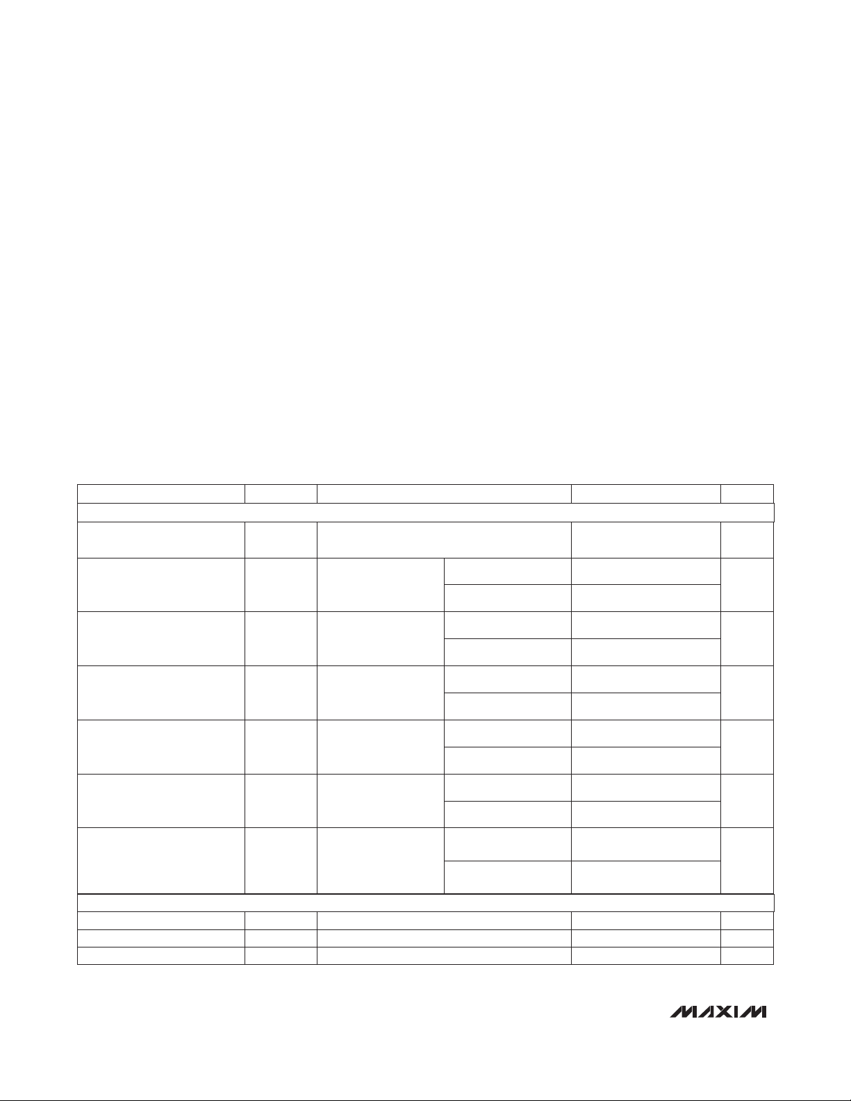
ELECTRICAL CHARACTERISTICS—Single +5V Supply
(V+ = +4.5V to +5.5V, VIH= 2.4V, VIL= 0.8V, TA= -40°C to +85°C, unless otherwise noted. Typical values are at V+ = +5V,
T
A
= +25°C.) (Notes 2, 3)
Stresses beyond those listed under “Absolute Maximum Ratings” may cause permanent damage to the device. These are stress ratings only, and functional
operation of the device at these or any other conditions beyond those indicated in the operational sections of the specifications is not implied. Exposure to
absolute maximum rating conditions for extended periods may affect device reliability.
(Voltages referenced to GND.)
V+ .............................................................................-0.3V to +6V
A_, EN, COM, NO_ (Note 1) .........................-0.3V to (V+ + 0.3V)
Continuous Current (all other pins) ..................................±20mA
Continuous Current (COM, NO_) .....................................±50mA
Peak Current (COM, NO_ pulsed at 1ms,
10% duty cycle) ........................................................±100mA
Continuous Power Dissipation (T
A
= +70°C)
10-Pin µMAX (derate 4.1mW/°C above +70°C) ..........330mW
10-Pin TDFN (derate 24.4mW/°C
above +70°C)............................................................1951mW
Operating Temperature Range ...........................-40°C to +85°C
Storage Temperature Range ............................-65°C to +150°C
Lead Temperature (soldering, 10s) ................................+300°C
V+ = 4.5V,
I
COM
= 10mA,
V
NO_
= 0 to V+
V+ = 5.5V;
V
COM
= 1V, 4.5V;
V
NO_
= 1V, 4.5V,
or unconnected
V+ = 4.5V,
I
COM
= 10mA,
V
NO_
= 0 to V+
V+ = 4.5V,
I
COM
= 10mA,
V
NO_
= 0 to V+
CONDITIONS
nA-100 5 +100Input Logic Current
V0.8V
IL
Input Logic-Low
V2.4V
IH
Input Logic-High
Ω
2.5 4
R
ON
On-Resistance
V0V+
V
COM
,
V
NO_
Analog Signal Range
DIGITAL INPUTS
-0.65 +0.65
I
COM(ON)
nA
-0.1 ±0.01 +0.1
COM On-Leakage Current
(Note 7)
1.2
4.5
Ω
0.1 0.3
ΔR
ON
On-Resistance Match
Between Channels
(Notes 4, 5)
0.4
Ω
0.75 1
R
FLAT(ON)
On-Resistance Flatness
(Note 6)
UNITSMIN TYP MAXSYMBOLPARAMETER
Note 1: Signals on NO_, COM, EN, or A_ exceeding V+ or GND are clamped by internal diodes. Limit forward diode current to maxi-
mum current rating.
TA= +25°C
TA= T
MIN
to T
MAX
TA= +25°C
TA= T
MIN
to T
MAX
TA= +25°C
TA= T
MIN
to T
MAX
TA= +25°C
V+ = 5.5V;
V
COM
= 1V, 4.5V;
V
NO_
= 4.5V, 1V
-0.3 +0.3TA= T
MIN
to T
MAX
nA
-0.1 ±0.01 +0.1
I
NO_(OFF)
NO_ Off-Leakage
Current (Note 7)
TA= +25°C
V+ = 5.5V;
V
COM
= 1V, 4.5V;
V
NO_
= 4.5V, 1V
-0.65 +0.65TA= T
MIN
to T
MAX
nA
-0.1 ±0.01 +0.1
I
COM(OFF)
COM Off-Leakage Current
(Note 7)
TA= +25°C
TA= T
MIN
to T
MAX
ANALOG SWITCH
DIGITAL I/O (A_, EN)
ABSOLUTE MAXIMUM RATINGS
Page 3
MAX4634
Fast, Low-Voltage, 4Ω,
4-Channel CMOS Analog Multiplexer
_______________________________________________________________________________________ 3
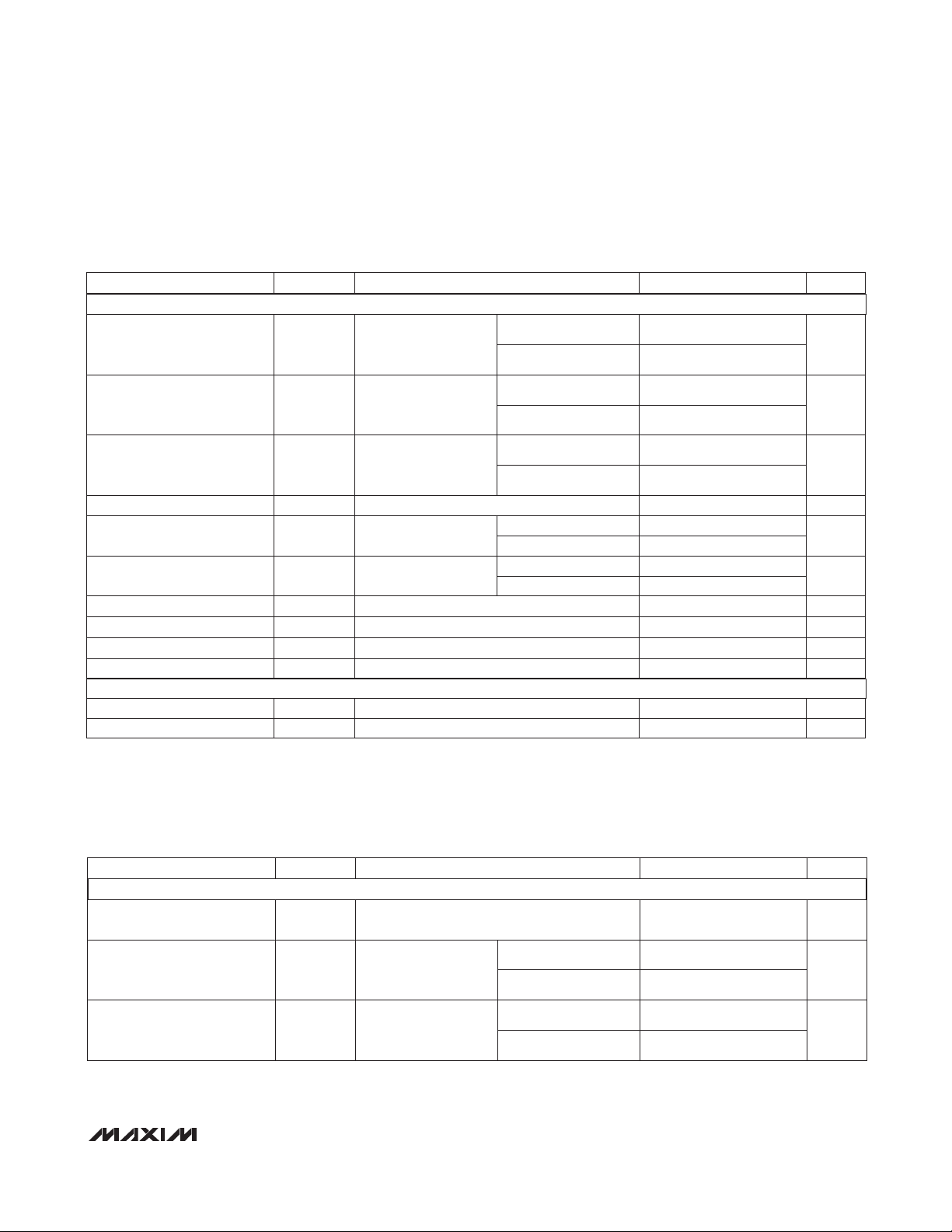
V
NO_
= 3V,
RL= 300Ω,
C
L
= 35pF, Figure 2
RL= 600Ω, f = 20Hz to 20kHz
CL= 5pF, RL= 50Ω,
Figure 5
TA= +25°C
V
NO_
= 3V,
R
L
= 300Ω,
CL= 35pF, Figure 2
TA= +25°C
V
NO_
= 3V,
RL= 300Ω,
CL= 35pF, Figure 3
V
GEN
= 2V, R
GEN
= 0, CL= 5pF, Figure 4
CONDITIONS
%0.018THDTotal Harmonic Distortion
dB
-80
V
ISO
Off-Isolation (Note 8)
pC2QCharge Injection
ns
14 18
t
ON
Turn-On Time (Note 7)
1
TA= T
MIN
to T
MAX
20
TA= +25°C
TA= T
MIN
to T
MAX
ns
611
t
OFF
Turn-Off Time (Note 7)
13
TA= T
MIN
to T
MAX
ns
8
t
BBM
Break-Before-Make Time
(Note 7)
UNITSMIN TYP MAXSYMBOLPARAMETER
V1.8 5.5V+Power-Supply Range
f = 1MHz
f = 10MHz
CL= 5pF, RL= 50Ω,
Figure 5
f = 1MHz
f = 10MHz
dB
-78
V
CT
Crosstalk (Note 9)
-57
-52
V+ = 2.7V,
I
COM
= 10mA,
V
NO_
= 0 to V+
TA= +25°C
V+ = 2.7V,
I
COM
= 10mA,
V
NO_
= 0 to V+
CONDITIONS
Ω
4.5 7
R
ON
On-Resistance
V0V+
V
COM
,
V
NO_
Analog Signal Range
TA= T
MIN
to T
MAX
8
TA= +25°C
TA= T
MIN
to T
MAX
Ω
0.1 0.3
ΔR
ON
0.4
UNITSMIN TYP MAXSYMBOLPARAMETER
ANALOG SWITCH
V+ = 5.5V, V
IH
= V+, VIL= 0 µA0.001 1.0I+Positive Supply Current
ELECTRICAL CHARACTERISTICS—Single +5V Supply (continued)
(V+ = +4.5V to +5.5V, VIH= 2.4V, VIL= 0.8V, TA= -40°C to +85°C, unless otherwise noted. Typical values are at V+ = +5V,
T
A
= +25°C.) (Notes 2, 3)
ELECTRICAL CHARACTERISTICS—Single +3V Supply
(V+ = +2.7V to +3.3V, VIH= 2.0V, VIL= 0.4V, TA= -40°C to +85°C, unless otherwise noted. Typical values are at V+ = +3V,
T
A
= +25°C.) (Notes 2, 3)
On-Resistance Match
Between Channels
(Notes 4, 5)
Figure 6 pF
52
C
NO_(OFF)
NO_ Off-Capacitance 13
pFFigure 6C
COM(OFF)
COM Off-Capacitance
68 pFCL= 5pF, Figure 6C
COM(ON)
COM On-Capacitance
DYNAMIC
POWER SUPPLY
Page 4

MAX4634
Fast, Low-Voltage, 4Ω,
4-Channel CMOS Analog Multiplexer
4 _______________________________________________________________________________________
CL= 5pF, RL= 50Ω,
Figure 5
V
GEN
= 1.5V, R
GEN
= 0, CL= 5pF, Figure 4
V
NO_
= 2V,
C
L
= 35pF,
R
L
= 300Ω, Figure 2
CL= 5pF, RL= 50Ω,
Figure 5
V
NO_
= 2V,
C
L
= 35pF,
R
L
= 300Ω, Figure 3
CONDITIONS
dB
-52
-80
V
ISO
Off-Isolation (Note 8) dB
-57
V0.4V
IL
Input Low
V2.0V
IH
Input High
pC2QCharge Injection
nA-100 5 +100Input Logic Current
ns
24
t
ON
Turn-On Time (Note 7)
ns
9
t
BBM
UNITSMIN TYP MAXSYMBOLPARAMETER
16 22
TA= T
MIN
to T
MAX
TA= +25°C
V
NO_
= 2V,
CL= 35pF,
RL= 300Ω, Figure 2
ns
16
t
OFF
Turn-Off Time (Note 7)
814
TA= T
MIN
to T
MAX
TA= +25°C
Break-Before-Make Time
(Note 7)
TA= +25°C
TA= T
MIN
to T
MAX
1
-78
V
CT
Crosstalk (Note 9)
f = 10MHz
f = 1MHz
f = 10MHz
f = 1MHz
V+ = 2.7V,
I
COM
= 10mA,
V
NO_
= 0 to V+
Ω
1.2 2.5
R
FLAT(ON)
On-Resistance Flatness
(Note 6)
TA= +25°C
TA= T
MIN
to T
MAX
3
V+ = 3.3V;
V
COM
= 1V, 3V;
V
NO_
= 3V, 1V
nA
-0.1 ±0.01 +0.1
I
NO_(OFF)
NO_ Off-Leakage Current
(Note 7)
TA= +25°C
TA= T
MIN
to T
MAX
-0.3 +0.3
V+ = 3.3V;
V
COM
= 1V, 3V;
V
NO_
= 3V, 1V
nA
-0.1 ±0.01 +0.1
I
COM(OFF)
COM Off-Leakage Current
(Note 7)
TA= +25°C
TA= T
MIN
to T
MAX
-0.65 +0.65
V+ = 3.3V;
V
COM
= 1V, 3V;
V
NO_
= 1V, 3V, or
unconnected
nA
-0.1 ±0.01 +0.1
I
COM(ON)
COM On-Leakage Current
(Note 7)
TA= +25°C
TA= T
MIN
to T
MAX
-0.65 +0.65
DIGITAL I/O (A_, EN)
DYNAMIC
ELECTRICAL CHARACTERISTICS—Single +3V Supply (continued)
(V+ = +2.7V to +3.3V, VIH= 2.0V, VIL= 0.4V, TA= -40°C to +85°C, unless otherwise noted. Typical values are at V+ = +3V,
T
A
= +25°C.) (Notes 2, 3)
Page 5

MAX4634
Fast, Low-Voltage, 4Ω,
4-Channel CMOS Analog Multiplexer
_______________________________________________________________________________________ 5
Note 2: The algebraic convention, where the most negative value is a minimum and the most positive value a maximum, is used in
this data sheet.
Note 3: TDFN parts are tested at +25°C and guaranteed by design and correlation over the entire temperature range.
Note 4: ΔR
ON
= R
ON(MAX)
- R
ON(MIN)
.
Note 5: R
ON
and ΔR
ON
matching specifications for TDFN-packaged parts are guaranteed by design.
Note 6: Flatness is defined as the difference between the maximum and minimum value of on-resistance as measured over the
specified analog signal ranges.
Note 7: Guaranteed by design.
Note 8: Off-isolation = 20log
10(VCOM
/ VNO), where V
COM
= output and VNO= input to off switch.
Note 9: Between any two switches.
20
15
10
5
0
021 345
ON-RESISTANCE vs. V
COM
MAX4634-01
V
COM
(V)
R
ON
(Ω)
V+ = 3.0V
V+ = 2.5V
V+ = 5.0V
V+ = 1.8V
5.0
4.5
4.0
3.5
3.0
2.5
0
1.0
0.5 2.01.5 2.5 3.0
ON-RESISTANCE vs. V
COM
AND
TEMPERATURE (V+ = +3V)
MAX4634-02
V
COM
(V)
R
ON
(Ω)
TA = +85°C
T
A
= -40°C
TA = +25°C
Typical Operating Characteristics
(TA= +25°C, unless otherwise noted.)
ELECTRICAL CHARACTERISTICS—Single +3V Supply (continued)
(V+ = +2.7V to +3.3V, VIH= 2.0V, VIL= 0.4V, TA= -40°C to +85°C, unless otherwise noted. Typical values are at V+ = +3V,
T
A
= +25°C.) (Notes 2, 3)
V
COM
= V
NO_
= GND, f = 1MHz, Figure 6
V
NO_
= GND, f = 1MHz, Figure 6
CONDITIONS
pF68C
(ON)
COM On-Capacitance
pF13C
NO_(OFF)
NO_ Off-Capacitance
UNITSMIN TYP MAXSYMBOLPARAMETER
V
COM
= GND, f = 1MHz, Figure 6 pF52C
COM(OFF)
COM Off-Capacitance
V+ = 3.3V, VIH= V+, VIL= 0 µA0.001 1I+Positive Supply Current
RL= 600Ω, f = 20Hz to 20kHz %0.018THDTotal Harmonic Distortion
POWER SUPPLY
4.0
3.5
3.0
2.5
2.0
1.5
0
2
1345
ON-RESISTANCE vs. V
COM
AND
TEMPERATURE (V+ = +5V)
MAX4634-03
V
COM
(V)
R
ON
(Ω)
T
A
= +85°C
T
A
= -40°C
T
A
= +25°C
Page 6

MAX4634
Fast, Low-Voltage, 4Ω,
4-Channel CMOS Analog Multiplexer
6 _______________________________________________________________________________________
-0.10
-0.05
0.05
0
0.10
0.15
ON/OFF-LEAKAGE CURRENT
vs. TEMPERATURE
MAX4634-04
TEMPERATURE (°C)
LEAKAGE (nA)
-50 500 100
I
COM(OFF)
I
NO_(OFF)
I
COM(ON)
2.0
1.5
1.0
0.5
0
1.5 3.02.0 2.5 3.5 4.0 4.5 5.0
LOGIC-LEVEL THRESHOLD
vs. SUPPLY VOLTAGE
MAX4634-10
SUPPLY VOLTAGE (V)
LOGIC-LEVEL THRESHOLD (V)
20
0.01 0.1 1 10 100 1000
0
-40
-20
-60
-80
-100
FREQUENCY RESPONSE
MAX4634-11
FREQUENCY (MHz)
LOSS (dB)
OFF-ISOLATION
CROSSTALK
BANDWIDTH
2.5
2.0
1.5
1.0
0.5
0
0
2
1345
CHARGE INJECTION vs. V
COM
MAX4634-05
V
COM
(V)
Q (pC)
V+ = 3V
V+ = 5V
35
30
25
20
15
10
5
0
1.5 2.5 3.02.0 3.5 4.0 4.5 5.0
ON/OFF-ENABLE TIME
vs. SUPPLY VOLTAGE
MAX4634-06
SUPPLY VOLTAGE (V)
t
ON/
t
OFF
(ns)
t
ON
t
OFF
12
10
8
6
4
2
0
-50 0 50 100
ON/OFF-ENABLE TIME
vs. TEMPERATURE
MAX4634-07
TEMPERATURE (°C)
t
ON/
t
OFF
(ns)
t
ON
t
OFF
0.5
0.4
0.3
0.2
0.1
0
-50
50
0 100 150
POWER-SUPPLY CURRENT
vs. TEMPERATURE
MAX4634-08
TEMPERATURE (°C)
I+, I
GND
(μA)
Typical Operating Characteristics (continued)
(TA= +25°C, unless otherwise noted.)
Page 7

MAX4634
Fast, Low-Voltage, 4Ω,
4-Channel CMOS Analog Multiplexer
_______________________________________________________________________________________ 7
Detailed Description
The MAX4634 is a low-on-resistance, low-voltage analog multiplexer that operates from a +1.8V to +5.5V single supply. CMOS switch construction allows processing of analog signals that are within the supply voltage range (GND to V+).
To disable all switch channels, drive EN low. All four inputs
and COM become high impedance during this state. If the
disable feature is not needed, connect EN to V+.
Applications Information
Power-Supply Sequencing and
Overvoltage Protection
Proper power-supply sequencing is recommended for
all CMOS devices. Always apply V+ before applying
analog signals or logic inputs, especially if the analog or
logic signals are not current limited. If this sequencing is
not possible, and if the analog or logic inputs are not
current limited to < 20mA, add a small-signal diode
(D1) as shown in Figure 1. If the analog signal can dip
below GND, add D2. Adding protection diodes reduces
the analog signal range to a diode drop (about 0.7V)
below V+ for D1 or to a diode drop above ground for D2.
The addition of diodes does not affect leakage. On-resistance increases by a small amount at low supply voltages.
Maximum supply voltage (V+) must not exceed 6V.
Protection diodes D1 and D2 also protect against some
overvoltage situations. A fault voltage up to the
absolute maximum rating at an analog signal input
does not damage the device, even if the supply voltage
is below the signal voltage.
Figure 1. Overvoltage Protection Using External Blocking Diodes
Pin Description
PIN
µMAX/
TDFN
FUNCTION
1A0
Address Input. See the
Truth Table
for details.
2 NO1 Normally Open Switch 1
3 GND Ground
4 NO3 Normally Open Switch 3
5EN
Enable Logic Input. See the
Truth
Table
for details.
6V+
Positive Supply Voltage. Connect
to an external power supply.
Bypass to GND with a 10µF
capacitor placed as close to the
pin as possible.
7 NO4 Normally Open Switch 4
8 COM Analog Switch Common Terminal
9 NO2 Normally Open Switch 2
10 A1
Address Input. See the
Truth Table
for details.
—EP
Exposed Pad. Internally connected
to GND. Connect to a large PCB
ground plane for proper operation.
Not intended as an electrical
connection point (TDFN package
only).
NAME
+5V
D1
V+
*
COM
*
GND
*
*
D2
*INTERNAL PROTECTION DIODES
MAX4634
NO
Page 8

MAX4634
Fast, Low-Voltage, 4Ω,
4-Channel CMOS Analog Multiplexer
8 _______________________________________________________________________________________
ΔV
OUT
+3V
0
LOGIC
INPUT
V
EN
+5V
V
OUT
GND
V+
A1
A0
EN
COM
MAX4634
CL = 5nF
V
OUT
NO
CHANNEL
SELECT
R
S
V
S
ONOFF OFF
ΔV
OUT
IS THE MEASURED VOLTAGE DUE TO CHARGE TRANSFER
ERROR Q WHEN THE CHANNEL TURNS OFF.
Q = ΔV
OUT x CL
V
EN
Figure 4. Charge Injection
50%
t
OPEN
tR < 5ns
t
F
< 5ns
+5V
VIH + 0.5V
0
LOGIC
INPUT
V
A_
SWITCH
OUTPUT
V
OUT
V+
V
OUT
GND
V+
A0
A1
EN
NO1–NO4
COM
+10V
50Ω
MAX4634
300Ω
35pF
90%
+2.4V
0
V
A
V
EN
Figure 3. Break-Before-Make Interval
Figure 2. Switching Time
50%
t
OFF
tR < 5ns
t
F
< 5ns
0
0
V
EN
= V
IH
+ 0.5
V
OUT
90%90%
t
ON
V+
V
OUT
GND
V+
A1
A0
EN
NO1
NO2–NO4
COM
V+
50Ω
300Ω
MAX4634
35pF
V
EN
V+
Test Circuits/Timing Diagrams
Page 9

MAX4634
Fast, Low-Voltage, 4Ω,
4-Channel CMOS Analog Multiplexer
_______________________________________________________________________________________ 9
Test Circuits/Timing Diagrams (continued)
MEASUREMENTS ARE STANDARDIZED AGAINST SHORTS AT SOCKET TERMINALS.
OFF-ISOLATION IS MEASURED BETWEEN COM AND “OFF” TERMINAL ON EACH SWITCH.
ON-LOSS IS MEASURED BETWEEN COM AND “ON” TERMINAL ON EACH SWITCH.
CROSSTALK IS MEASURED BETWEEN COMA AND COMB TERMINALS ON EACH DEVICE.
SIGNAL DIRECTION THROUGH SWITCH IS REVERSED; WORST VALUES ARE RECORDED.
NOTES:
V+
V+
V+
V
OUT
GND
V+
A
EN
NO
COM
V
IN
MAX4634
OFF-ISOLATION = 20log
V
OUT
V
IN
ON-LOSS = 20log
V
OUT
V
IN
CROSSTALK = 20log
V
OUT
V
IN
NETWORK
ANALYZER
50Ω
50Ω 50Ω
50Ω
MEAS REF
10nF
+5V
GND
V+
A1
A0
NO4
MAX4634
CHANNEL
SELECT
NO1
COM
EN
1MHz
CAPACITANCE
ANALYZER
f = 1MHz
Figure 5. Off-Isolation/On-Channel Bandwidth
Figure 6. Channel Off/On-Capacitance
Chip Information
PROCESS: CMOS
Package Information
For the latest package outline information and land patterns, go
to www.maxim-ic.com/packages
.
PACKAGE TYPE PACKAGE CODE DOCUMENT NO.
10 µMAX —
21-0061
10 TDFN T1033-1
21-0137
Page 10

MAX4634
Fast, Low-Voltage, 4Ω,
4-Channel CMOS Analog Multiplexer
Maxim cannot assume responsibility for use of any circuitry other than circuitry entirely embodied in a Maxim product. No circuit patent licenses are
implied. Maxim reserves the right to change the circuitry and specifications without notice at any time.
10
____________________Maxim Integrated Products, 120 San Gabriel Drive, Sunnyvale, CA 94086 408-737-7600
© 2009 Maxim Integrated Products Maxim is a registered trademark of Maxim Integrated Products, Inc.
Revision History
REVISION
NUMBER
DATE
DESCRIPTION
PAGES
CHANGED
0 4/00 Initial release —
1 2/02 Added QFN package —
2 5/03 Added QFN packaging information —
3 2/09 Added TDFN package information (replaced QFN), style edits 1, 7
REVISION
 Loading...