

Page 1
For free samples & the latest literature: http://www.maxim-ic.com, or phone 1-800-998-8800.
For small orders, phone 1-800-835-8769.
General Description
The MAX4631/MAX4632/MAX4633 high-voltage, dual
analog switches are pin compatible with the industry-standard DG401/DG403/DG405. They upgrade the existing
devices with fault-protected inputs and Rail-to-Rail®signal
handling capabilities. The MAX4631/MAX4632/MAX4633’s
normally open (NO) and normally closed (NC) terminals
are protected from overvoltage faults up to 36V during
power-up or power-down. During a fault condition, these
terminals become open circuit and only nanoamperes of
leakage current flow from the source, yet the switch output
(COM_) continues to furnish up to 18mA of the appropriate polarity supply voltage to the load. This ensures unambiguous rail-to-rail outputs when a fault begins and ends.
On-resistance is 85Ω (max) at +25°C and is matched
between switches to 6Ω (max). Off-leakage current is only
0.5nA at +25°C and 5nA at +85°C.
The MAX4631 has two NO single-pole/single-throw (SPST)
switches. The MAX4632 has two NO/NC single-pole/
double-throw (SPDT) switches. The MAX4633 has two NO
double-pole/single-throw (DPST) switches.
These CMOS switches operate with dual power supplies
ranging from ±4.5V to ±18V or a single supply between
+9V and +36V. All digital inputs have +0.8V and +2.4V
logic thresholds, ensuring both TTL- and CMOS-logic
compatibility when using ±15V or a single +12V supply.
Applications
ATE Equipment
Data Acquisition
Industrial and Process Control Systems
Avionics
Redundant/Backup Systems
Features
♦ Fault Protection
±40V with Power Off
±36V with ±15V Supplies (MAX4631/MAX4633)
±25V with ±15V Supplies (MAX4632)
♦ Rail-to-Rail Signal Handling
♦ No Power-Supply Sequencing Required
♦ All Switches Off with Power Off
♦ Output Clamped to Appropriate Supply Voltage
During Fault Condition; No Transition Glitch
♦ 85Ω (max) Signal Paths with ±15V Supplies
♦ ±4.5V to ±18V Dual Supplies
+9V to +36V Single Supply
♦ Low Power Consumption: <6mW
♦ Pin Compatible with Industry-Standard
DG401/DG403/DG405
♦ TTL- and CMOS-Logic Compatible Inputs with
Single +9V to +15V, or ±15V Supplies
MAX4631/MAX4632/MAX4633
Fault-Protected, High-Voltage,
Dual Analog Switches
________________________________________________________________
Maxim Integrated Products
1
19-1515; Rev 0; 7/99
Ordering Information
Rail-to-Rail is a registered trademark of Nippon Motorola, Ltd.
Pin Configurations appear at end of data sheet.
PART
MAX4631CSE
MAX4631CPE
MAX4631ESE -40°C to +85°C
0°C to +70°C
0°C to +70°C
TEMP. RANGE PIN-PACKAGE
16 Narrow SO
16 Plastic DIP
16 Narrow SO
MAX4631EPE
MAX4631MJE
MAX4632CSE
0°C to +70°C
-55°C to +125°C
-40°C to +85°C 16 Plastic DIP
16 CERDIP
16 Narrow SO
MAX4632CPE
MAX4632ESE
MAX4632EPE -40°C to +85°C
-40°C to +85°C
0°C to +70°C 16 Plastic DIP
16 Narrow SO
16 Plastic DIP
MAX4632MJE
MAX4633CSE
MAX4633CPE 0°C to +70°C
0°C to +70°C
-55°C to +125°C 16 CERDIP
16 Narrow SO
16 Plastic DIP
MAX4633ESE
MAX4633EPE
MAX4633MJE -55°C to +125°C
-40°C to +85°C
-40°C to +85°C 16 Narrow SO
16 Plastic DIP
16 CERDIP
Page 2
MAX4631/MAX4632/MAX4633
Fault-Protected, High-Voltage,
Dual Analog Switches
2 _______________________________________________________________________________________
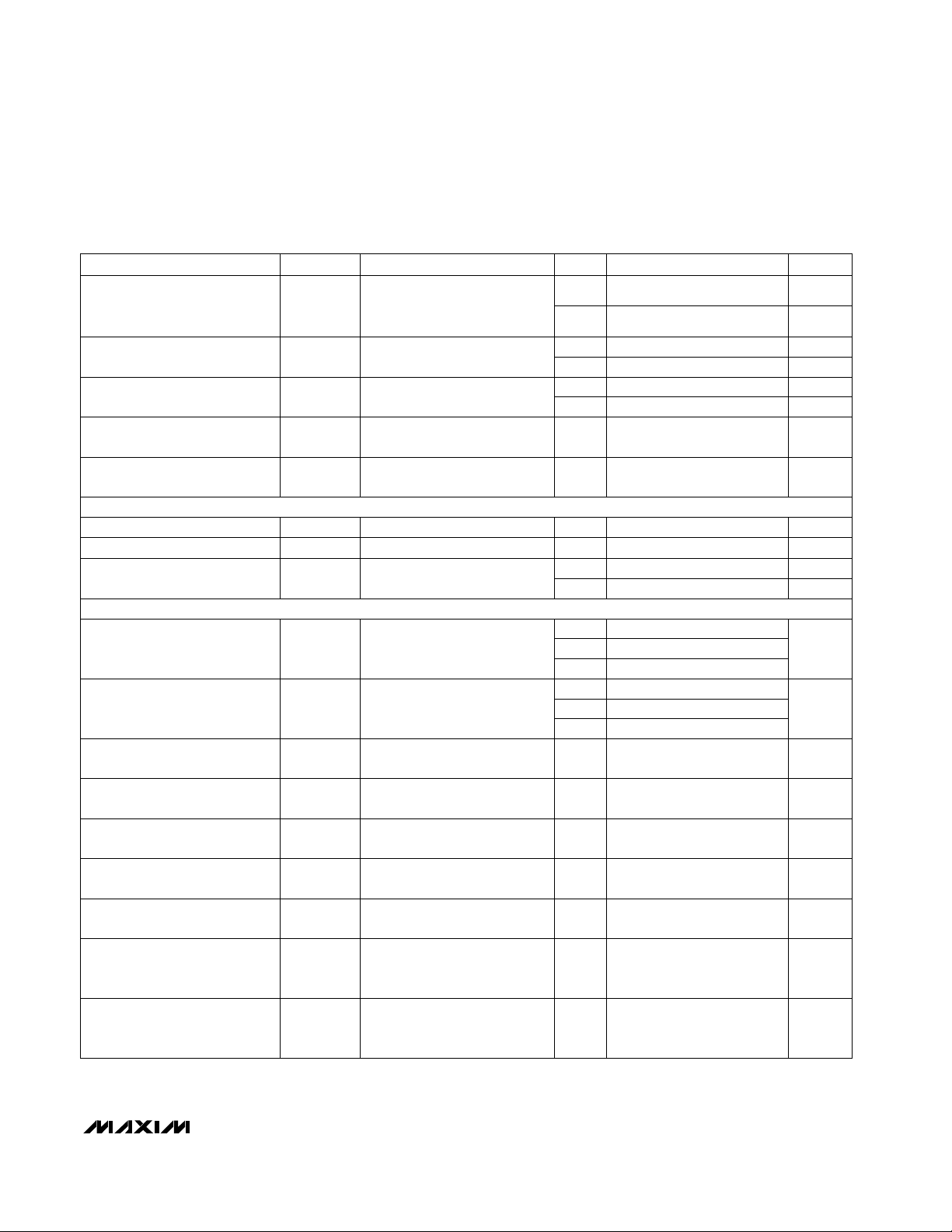
ABSOLUTE MAXIMUM RATINGS
ELECTRICAL CHARACTERISTICS—Dual Supplies
(V+ = +15V, V- = -15V, V
INL_
= 0.8V, V
INH_
= 2.4V, TA= T
MIN
to T
MAX
, unless otherwise noted. Typical values are at TA = +25°C.) (Note 3)
Stresses beyond those listed under “Absolute Maximum Ratings” may cause permanent damage to the device. These are stress ratings only, and functional
operation of the device at these or any other conditions beyond those indicated in the operational sections of the specifications is not implied. Exposure to
absolute maximum rating conditions for extended periods may affect device reliability.
(Voltages referenced to GND)
V+...........................................................................-0.3V to +44V
V- ............................................................................-44V to +0.3V
V+ to V-...................................................................-0.3V to +44V
COM_, IN_ (Note 1) ..............................(V- - 0.3V) to (V+ + 0.3V)
NC_, NO_ (Note 2)
MAX4631_ _E .....................................(V+ - 36V) to (V- + 36V)
MAX4632_ _E .....................................(V+ - 25V) to (V- + 25V)
MAX4633_ _E .....................................(V+ - 36V) to (V- + 36V)
NC_, NO_ to COM_
MAX4631_ _E ......................................................-36V to +36V
MAX4632_ _E ......................................................-25V to +25V
MAX4633_ _E ......................................................-36V to +36V
Continuous Current into Any Terminal..............................±30mA
Peak Current into Any Terminal (pulsed at 1ms,
10% duty cycle)............................................................±50mA
Continuous Power Dissipation (TA= +70°C) (Note 2)
Plastic DIP (derate 10.53mW/°C above +70°C) ..........842mW
Narrow SO (derate 8.70mW/°C above +70°C) ............696mW
CERDIP (derate 10.00mW/°C above +70°C)...............842mW
Operating Temperature Ranges
MAX463_C_E ......................................................0°C to +70°C
MAX463_E_E ...................................................-40°C to +85°C
MAX463_M_E ................................................-55°C to +125°C
Storage Temperature Range .............................-65°C to +150°C
Lead Temperature (soldering, 10sec) .............................+300°C
Note 1: COM_ and IN_ pins are not fault protected. Signals on COM_ to IN_ exceeding V+ or V- are clamped by internal diodes.
Limit forward diode current to maximum current rating.
Note 2: NC_ and NO_ pins are fault protected (see
Electrical Characteristics
). With power applied to V+ or V-, signals on NC_ or
NO_ exceeding ±25V (MAX4632) or ±36V (MAX4631/MAX4633) may damage the device. With V+ = V- = 0, signals on NC_
or NO_ exceeding ±40V may damage the device.
T
A
PARAMETER SYMBOL MIN TYP MAX UNITSCONDITIONS
C, E, M
Fault-Free Analog Signal Range
(Note 2)
V
NO_,VNC_
V- V+ V
C, E 100
M 200
Ω
+25°C
COM_ to NO_ or NC_
On-Resistance
R
ON
62 85
V
COM_
= ±10V,
I
COM_
= 1mA
C, E 10
M 15
Ω
+25°C
COM_ to NO_ or NC_
On-Resistance Match
Between Channels (Note 4)
∆R
ON
36
V
COM_
= ±10V,
I
COM_
= 1mA
C, E -5 5
M -100 100
nA
+25°C
NO_, NC_, COM_ Off-Leakage
Current (Note 5)
I
NO_ (OFF)
,
I
NC_ (OFF)
,
I
COM_(OFF)
-0.5 0.01 0.5
V
COM_
= ±14V,
V
NO_
or V
NC_
=
−
+14V
C, E -20 20
M -100 100
nA
+25°C
COM_ On-Leakage Current
(Note 5)
I
COM_(ON)
-0.5 0.01 0.5
V
COM_
= ±14V,
V
NO_
or V
NC_
= ±14V
or floating
C, E, M -36 36
V
Fault-Protected Analog
Signal Range (Note 2)
V
NO_
, V
NC_
Applies with
power on
C, E, M -25 25
C, E, M -40 40Applies with power off
MAX4631/
MAX4633
MAX4632
ANALOG SWITCH
FAULT PROTECTION
Page 3
MAX4631/MAX4632/MAX4633
Fault-Protected, High-Voltage,
Dual Analog Switches
_______________________________________________________________________________________ 3
ELECTRICAL CHARACTERISTICS—Dual Supplies (continued)
(V+ = +15V, V- = -15V, V
INL_
= 0.8V, V
INH_
= 2.4V, TA= T
MIN
to T
MAX
, unless otherwise noted. Typical values are at TA = +25°C.) (Note 3)
C, E -200 200
M -10 10
nA
+25°C
T
A
C, E
NO_ or NC_ Input Leakage
Current, Supplies On
I
NO_
, I
NC_
PARAMETER SYMBOL MIN TYP MAX UNITS
-200 200
-20 20
V
NO_
or V
NC_
= ±25V,
V
COM_
= ±10V
M
C, E -200 200
-1 1
nA
M
CONDITIONS
+25°C
COM_ Output Leakage Current,
Supplies On
I
COM_
-10 10
-10 10
V
NO_
or V
NC_
= ±25V,
no connection to “on” channel
(MAX4632 only)
nA
+25°C
NO_ or NC_ Input Leakage
Current, Supplies Off
I
NO_
, I
NC_
-20 20
V
NO_
or V
NC_
= ±40V,
-24 -18 13
mA
+25°C
COM_ Output Clamp Current,
Supplies On
I
COM_
13 18 24V
NO_
or V
NC_
= +25V
C, E, M 2.4 VIN_ Input Logic Voltage High V
INH_
C, E, M -5 5
µA
µA
µA
+25°CV
NO_
or V
NC_
= -25V
kΩ+25°C
COM_ Output Clamp Resistance,
Supplies On
R
COM_
0.5 1V
NO_
or V
NC_
= ±25V
C, E, M 0.8 VIN_ Input Logic Voltage Low V
INL_
+25°C -1 0.03 1
µA
IN_ Input Current Logic
High or Low
I
INH_
, I
INL_VIN_
= 0.8V or 2.4V
ns
+25°C 100 150
V
COM_
= ±10V, RL= 1kΩ,
Figure 2
t
ON
C, E, 500Turn-On Time
M 600
ns
+25°C 50 100
V
COM_
= ±10V, RL= 1kΩ,
Figure 2
t
OFF
C, E, 400Turn-Off Time
M 500
ns+25°C 10 40
V
COM_
= ±10V, RL= 1kΩ,
Figure 3
t
BBM
Break-Before-Make Time Delay
(MAX4632 only)
pC+25°C 510
CL= 100pF, Figure 4,
NO_ = NC_ = GND, RS= 0
QCharge Injection (Note 6)
pFC, E, M 18
NO_ = NC_ = GND, f = 1MHz,
Figure 5
C
NC_(OFF)
,
C
NO_(OFF)
NO_, NC_ Off- Capacitance
pFC, E, M 18
COM_ = GND, f = 1MHz,
Figure 5
C
COM_(OFF)
COM_ Off-Capacitance
pFC, E, M 22
COM_ = NO_ = NC_ = GND,
f = 1MHz, Figure 5
C
COM_(ON)
COM_ On-Capacitance
LOGIC INPUT
SWITCH DYNAMIC CHARACTERISTICS
Page 4
MAX4631/MAX4632/MAX4633
Fault-Protected, High-Voltage,
Dual Analog Switches
4 _______________________________________________________________________________________
C, E, M
VC, E, M
T
A
Power-Supply Range V+, V-
PARAMETER SYMBOL MIN TYP MAX UNITS
±4.5 ±18
C, E, M 550
dB
CONDITIONS
C, E, M
Off-Isolation
(Note 7)
V
ISO
-62
RL= 50Ω, CL= 15pF,
V
NO_
= V
NC_
= 1V
RMS
,
f = 1MHz, Figure 6
µA
+25°C
V+ Supply Current
I+
230 325
All V
IN_
= 0 or 5V,
V
NO_
or V
NC_
= 0
10
µA
+25°C
GND Supply Current I
GND
-1 0.01 1
All V
IN_
= 0 or 15V,
V
NO_
or V
NC_
= 0
dBC, E, M
Channel-to-Channel Crosstalk
(Note 8)
V
CT
-66
RL= 50Ω, CL= 15pF,
V
NO_
= V
NC_
= 1V
RMS
,
f = 1MHz, Figure 7
C, E, M 300
µA
+25°C
V- Supply Current
I-
130 200
All V
IN_
= 0 or 5V,
V
NO_
or V
NC_
= 0
C, E, M 300
+25°C 125 175
All V
IN_
= 5V,
V
NO_
or V
NC_
= 0
C, E, M
Fault-Free Analog Signal Range
(Note 2)
V
NO_
, V
NC_
0V+V
C, E 20
M 30
Ω
+25°C
T
A
C, E
COM_ to NO_ or NC_
On-Resistance Match
Between Channels (Note 4)
∆R
ON
PARAMETER SYMBOL MIN TYP MAX UNITS
250
410
V
COM_
= 10V,
I
COM_
= 1mA
M
C, E -10 10
300
Ω
M
CONDITIONS
+25°C
COM_ to NO_ or NC_
On-Resistance
R
ON
125 200
-200 200
V
COM_
= 10V,
I
COM_
= 1mA
nA
+25°C
NO_, NC_, COM_ Off-Leakage
Current (Notes 5, 9)
I
NO_ (OFF)
,
I
NC_ (OFF)
-0.5 0.01 0.5
V
COM_
= 10V,
V
NO_
or V
NC_
= 12V
C, E -20 20
M -400 400
nA
+25°C
COM_ On-Leakage Current
(Notes 5, 9)
I
COM_(ON)
-0.5 0.01 0.5
V
COM_
= 10V,
V
NO_
or V
NC_
= 1V or 12V
C, E, M -36 36
MAX4632
V
Fault-Protected Analog
Signal Range (Note 2)
V
NO_
, V
NC_
Applies with
power on
C, E, M -25 25
C, E, M -40 40Applies with power off
MAX4631/
MAX4633
ELECTRICAL CHARACTERISTICS—Dual Supplies (continued)
(V+ = +15V, V- = -15V, V
INL_
= 0.8V, V
INH_
= 2.4V, TA= T
MIN
to T
MAX
, unless otherwise noted. Typical values are at TA = +25°C.) (Note 3)
ELECTRICAL CHARACTERISTICS—Single Supply
(V+ = +15V, V- = -15V, V
INL_
= 0.8V, V
INH_
= 2.4V, TA= T
MIN
to T
MAX
, unless otherwise noted. Typical values are at TA = +25°C.) (Note 3)
POWER SUPPLY
ANALOG SWITCH
FAULT PROTECTION
Page 5
V
IN_
= 0.8V or 2.4V
MAX4631/MAX4632/MAX4633
Fault-Protected, High-Voltage,
Dual Analog Switches
_______________________________________________________________________________________ 5
µA
µA
ns
C, E -100 100
M -10 10
nA
T
A
C, E
I
NO_
, I
NC_
PARAMETER SYMBOL MIN TYP MAX UNITS
-10 10
V
NO_
or V
NC_
= ±25V,
V
COM_
= ±10V
M -1 1
nA
CONDITIONS
COM_ Output Leakage Current,
Supplies On
I
COM_
V
NO_
or V
NC_
= ±25V,
no connection to “on” channel
(MAX4632 only)
+25°C
kΩ
mA+25°C
COM_ Output Clamp Current,
Supplies On
I
COM_
4 5.5 10V
NO_
or V
NC_
= 25V
C, E, M 2.4
140 250
+25°C
VIN_ Input Logic Voltage High V
INH_
C, E, M
C, E, M -5 5
COM_ Output Clamp Resistance,
Supplies On
R
COM_
1 2.5
V
COM_
= ±10V, RL= 2kΩ,
Figure 2
V
NO_
or V
NC_
= 25V
t
ON
ns
0.8 VIN_ Input Logic Voltage Low V
INL_
+25°C -1 0.03 1 µA
IN_ Input Current Logic
High or Low
I
INH_
, I
INL_VIN_
= 0.8V or 2.4V
+25°C 100 200
C, E, 300
V
COM_
= ±10V, RL= 2kΩ,
Figure 2
t
OFF
C, E,
Turn-On Time
250
M 500
Turn-Off Time
pC
M 400
ns+25°C 540
V
COM_
= ±10V, RL= 2kΩ,
Figure 3
t
BBM
+25°C 5
Break-Before-Make Time Delay
(MAX4632 only)
CL= 100pF, Figure 4,
NO_ = NC_ = GND, RS= 0
QCharge Injection (Note 6)
pFC, E, M 20
NO_ = NC_ = GND,
f = 1MHz, Figure 5
C
NC_(OFF)
,
C
NO_(OFF)
NO_, NC_ Off-Capacitance
pFC, E, M 20
COM_ = GND, f = 1MHz,
Figure 5
C
COM_(OFF)
COM_ Off-Capacitance
pFC, E, M 25
COM_ = NO_ = NC_ = GND,
f = 1MHz, Figure 5
C
COM_(ON)
COM_ On-Capacitance
ELECTRICAL CHARACTERISTICS—Single Supply (continued)
(V+ = +15V, V- = -15V, V
INL_
= 0.8V, V
INH_
= 2.4V, TA= T
MIN
to T
MAX
, unless otherwise noted. Typical values are at TA = +25°C.) (Note 3)
NO_ or NC_ Input Leakage
Current, Supplies On
dBC, E, M -62
RL= 50Ω, CL= 15pF,
V
NO_
= V
NC_
= 1V
RMS
,
f = 1MHz, Figure 6
V
ISO
Off-Isolation
(Note 7)
dBC, E, M -65
RL= 50Ω, CL= 15pF,
V
NO_
= V
NC_
= 1V
RMS
,
f = 1MHz, Figure 7
V
CT
Channel-to-Channel Crosstalk
(Note 8)
µA
C, E -100 1 100
M -10 10
nA
I
NO_
, I
NC_VNO_
or V
NC_
= ±40V
NO_ or NC_ Input Leakage
Current, Supplies Off
LOGIC INPUT
µA
SWITCH DYNAMIC CHARACTERISTICS
Page 6

0
40
20
80
60
120
100
140
180
160
200
-20 -10 -5-15 0 5 10 15 20
SWITCH ON-RESISTANCE vs. V
COM
(DUAL SUPPLIES)
MAX4631-33 toc01
V
COM
(V)
ON-RESISTANCE (Ω)
V+ = +5V
V- = -5V
V+ = +10V
V- = -10V
V+ = +12V
V- = -12V
V+ = +15V
V- = -15V
V+ = +20V
V- = -20V
0
40
20
80
60
100
120
-15 -5 0-10 5 10 15
ON-RESISTANCE vs. V
COM
AND TEMPERATURE (DUAL SUPPLIES)
MAX4631-33 toc02
V
COM
(V)
ON-RESISTANCE (Ω)
TA = +85°C
TA = +25°C
TA = -40°C
TA = -55°C
V+ = 15V
V- = -15V
TA = +125°C
50
150
100
300
250
200
450
400
350
500
0105 15202530
SWITCH ON-RESISTANCE
vs. V
COM
(SINGLE SUPPLY)
MAX4631-33 toc03
V
COM
(V)
ON-RESISTANCE (Ω)
V- = GND
V+ = +5V
V+ = +8V
V+ = +12V
V+ = +15V
V+ = +20V
V+ = +24V
V+ = +30V
Typical Operating Characteristics
(TA = +25°C, unless otherwise noted.)
MAX4631/MAX4632/MAX4633
Fault-Protected, High-Voltage,
Dual Analog Switches
6 _______________________________________________________________________________________
VC, E, M
T
A
Power-Supply Range V+, V-
PARAMETER SYMBOL MIN TYP MAX UNITS
036
C, E, M 400
CONDITIONS
µA
+25°C
V+ Supply Current
I+
165 250
All V
IN_
= 0 or 5V,
V
NO_
or V
NC_
= 0
ELECTRICAL CHARACTERISTICS—Single Supply (continued)
(V+ = +15V, V- = -15V, V
INL_
= 0.8V, V
INH_
= 2.4V, TA= T
MIN
to T
MAX
, unless otherwise noted. Typical values are at TA = +25°C.) (Note 3)
C, E, M 400
µA
+25°C
GND Supply Current I
GND
165 250
All V
IN_
= 0 or 5V,
V
NO_
or V
NC_
= 0
Note 2: NC_ and NO_ pins are fault protected (see
Electrical Characteristics
). With power applied to V+ or V-, signals on NC_ or
NO_ exceeding ±25V (MAX4632) or ±36V (MAX4631/MAX4633) may damage the device. With V+ = V- = 0, signals on NC_
or NO_ exceeding ±40V may damage the device.
Note 3: The algebraic convention is used in this data sheet; the most negative value is shown in the minimum column.
Note 4: ∆R
ON
= R
ON(MAX)
- R
ON(MIN)
.
Note 5: Leakage parameters are 100% tested at maximum rated hot temperature and guaranteed by correlation at +25°C.
Note 6: Guaranteed by design.
Note 7: Off-isolation = 20log
10[VCOM_
/ (V
NC_
or V
NO_
)], V
COM_
= output, V
NC_
or V
NO_
= input to off switch.
Note 8: Between any two switches.
Note 9: Leakage testing for single-supply operation is guaranteed by testing with dual supplies.
POWER SUPPLY
Page 7

MAX4631/MAX4632/MAX4633
Fault-Protected, High-Voltage,
Dual Analog Switches
_______________________________________________________________________________________
7
Typical Operating Characteristics (continued)
(TA= +25°C, unless otherwise noted.)
ON-RESISTANCE vs. V
AND TEMPERATURE (SINGLE SUPPLY)
250
V+ = +12V
230
210
190
170
150
130
ON-RESISTANCE (Ω)
110
90
70
TA = -40°C
50
042681012
TA = +25°C
TA = +85°C
V
COM
SUPPLY CURRENT vs. V
250
200
150
100
SUPPLY CURRENT (µA)
50
0
0462 8 10 12 14 16
I+
VIN (V)
TA = +125°C
(V)
I-
I
GND
COM
TA = -55°C
IN
V+ = +15V
V- = -15V
3.0
2.8
2.6
MAX4631-33 toc04
2.4
2.2
2.0
1.8
1.6
LOGIC-LEVEL THRESHOLD (V)
1.4
1.2
1.0
010155 2025303540
250
200
MAX4631-33 toc07
150
I+ (µA)
100
50
0
0462 8 10 12 14 16
LOGIC-LEVEL THRESHOLD vs. V+
SINGLE OR DUAL SUPPLY
V+ (V)
I+ vs. V
IN
DUAL SUPPLIES
V+ = +15V
V- = -15V
SINGLE SUPPLY
V+ = +12V
V- = GND
VIN (V)
MAX4631-33 toc05
SUPPLY CURRENT (µA)
MAX4631-33 toc08
LOSS (dB)
-100
-110
-120
SUPPLY CURRENT vs. TEMPERATURE
200
180
160
140
120
100
80
60
40
20
0
-55 -15 5 25-35 45 65 85 105 125
DUAL SUPPLIES
V+ = +15V
V- = -15V
SINGLE SUPPLY
V+ = +12V
V- = GND
TEMPERATURE (°C)
FREQUENCY RESPONSE
0
-10
-20
-30
-40
-50
-60
-70
-80
-90
ON-LOSS
OFF-LOSS
0.01 0.1 1
FREQUENCY (MHz)
ON-PHASE
10 100 1000
MAX4631-33 toc06
120
100
80
MAX4631-33 toc09
60
40
20
0
-20
PHASE (DEGREES)
-40
-60
-80
-100
-120
CHARGE INJECTION vs. V
30
25
20
15
10
5
CHARGE INJECTION (pC)
0
-5
DUAL SUPPLIES
V+ = +15V
V- = -15V
SINGLE SUPPLY
V+ = +12V
-10
-15 -5-10 0 5 10 15
V
(V)
COM
COM
500
450
400
MAX4631-33 toc10
350
300
250
TIME (ns)
200
150
100
ON/OFF TIME
vs. SINGLE-SUPPLY VOLTAGE
NO_ t
ON
NC_ t
ON
NO_ t
OFF
50
NC_ t
0
OFF
0126 18243036
SUPPLY VOLTAGE (V)
MAX4631-33 toc11
TIME (ns)
ON/OFF TIME
vs. DUAL-SUPPLY VOLTAGE
450
400
350
300
250
200
150
NO_ t
100
50
0
042 6 8 101214161820
NO_ t
OFF
NC_ t
OFF
SUPPLY VOLTAGE (V)
ON
NC_ t
ON
MAX4631-33 toc12
Page 8
MAX4631/MAX4632/MAX4633
Fault-Protected, High-Voltage,
Dual Analog Switches
8 _______________________________________________________________________________________
Typical Operating Characteristics (continued)
(TA= +25°C, unless otherwise noted.)
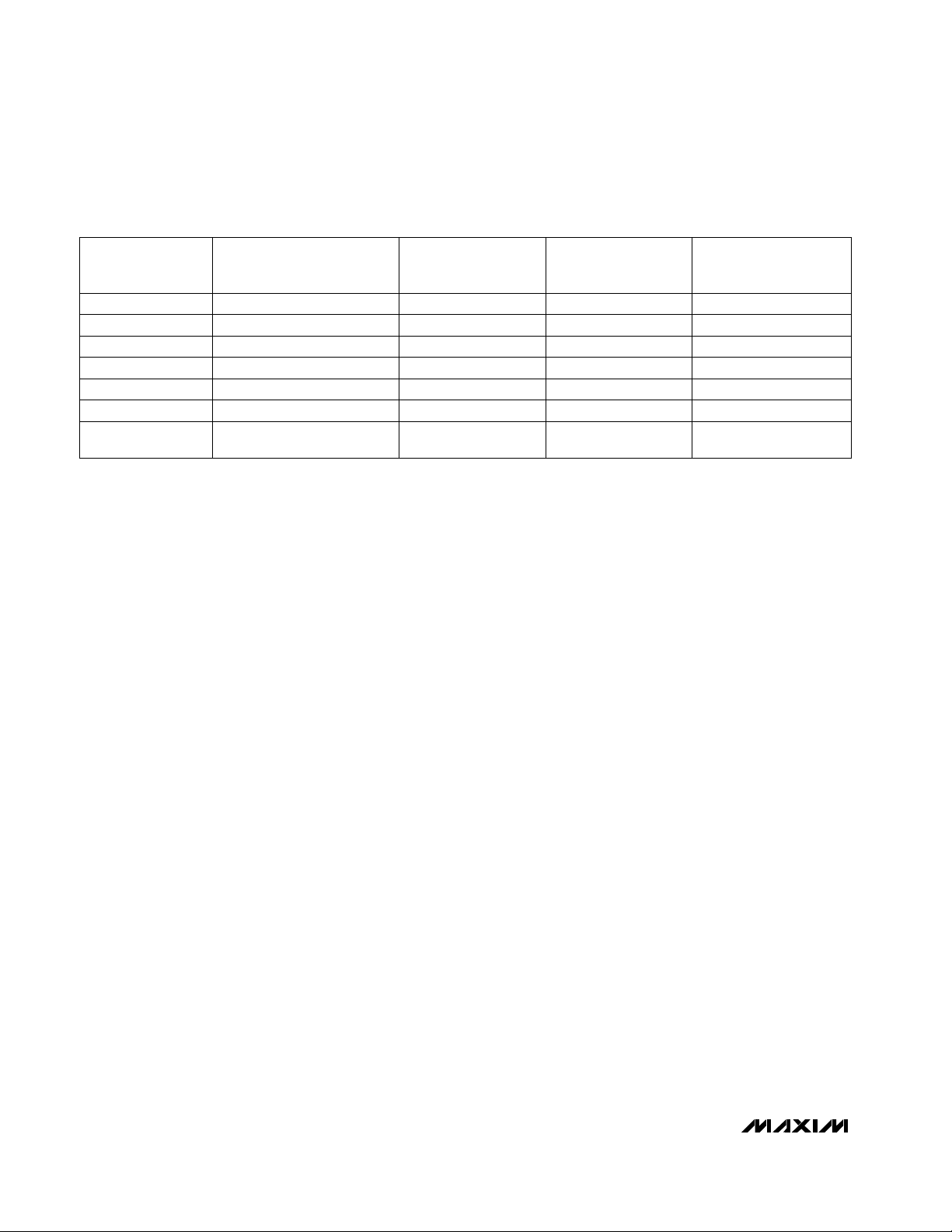
Pin Description
FUNCTION
16, 9 16, 9 Analog Switch Normally Open Terminals
15, 10 15, 10 Logic-Control Digital Inputs
2–7, 12 2, 7, 12 No Connection. Not internally connected.
— 3, 6 Analog Switch Common Terminals
— 4, 5 Analog Switch Normally Closed Terminals
— — Analog Switch Normally Open Terminals
11 11 Positive Supply Input
16, 9
15, 10
2, 7, 12
3, 6
—
4, 5
11
NAME
NO1, NO2
IN1, IN2
N.C.
COM3, COM4
NC3, NC4
NO3, NO4
V+
13 13 Ground
14 14 Negative Supply Input
13
14
GND
V-
1, 8 1, 8 Analog Switch Common Terminals1, 8 COM1, COM2
MAX4631 MAX4632 MAX4633
PIN
0.01
0.1
1
10
100
1000
-55 5 25-35 -15 45 65 85 105 125
LEAKAGE CURRENT vs. TEMPERATURE
MAX4631-33 toc13
TEMPERATURE (°C)
LEAKAGE CURRENT (nA)
INO
(OFF)
AT
V
NO
= +14V,
V
COM
= -14V
INO
(OFF)
AT
V
NO
= -14V,
V
COM
= +14V
I
COM (ON)
AT
V
COM
= +14V
I
COM (OFF)
AT
V
NO
= -14V,
V
COM
= +14V
I
COM (OFF)
AT
V
NO
= +14V,
V
COM
= -14V
I
COM (ON)
AT
V
COM
= -14V
50
70
90
110
130
150
170
-55 -15-35 5 25 45 65 85 105 125
ON/OFF TIME vs. TEMPERATURE
MAX4631-33 toc14
TEMPERATURE (°C)
TIME (ns)
t
ON
t
OFF
0
-20
+20
0
+10
-10
-20
+20
INPUT OVERVOLTAGE vs.
OUTPUT CLAMPING (±15V SUPPLIES)
MAX4631-33 toc15
(20µs/div)
INPUT OVERVOLTAGE (V)
OUTPUT CLAMPING
V
NO
V
COM
0
-10
+10
+10
-10
FAULT-FREE SIGNAL
(±15V SUPPLIES)
MAX4631-33 toc16
0
INPUT OVERVOLTAGE (V)
(20µs/div)
OUTPUT CLAMPING
V
COM
V
NO
Page 9
MAX4631/MAX4632/MAX4633
Fault-Protected, High-Voltage,
Dual Analog Switches
_______________________________________________________________________________________ 9
_______________Detailed Description
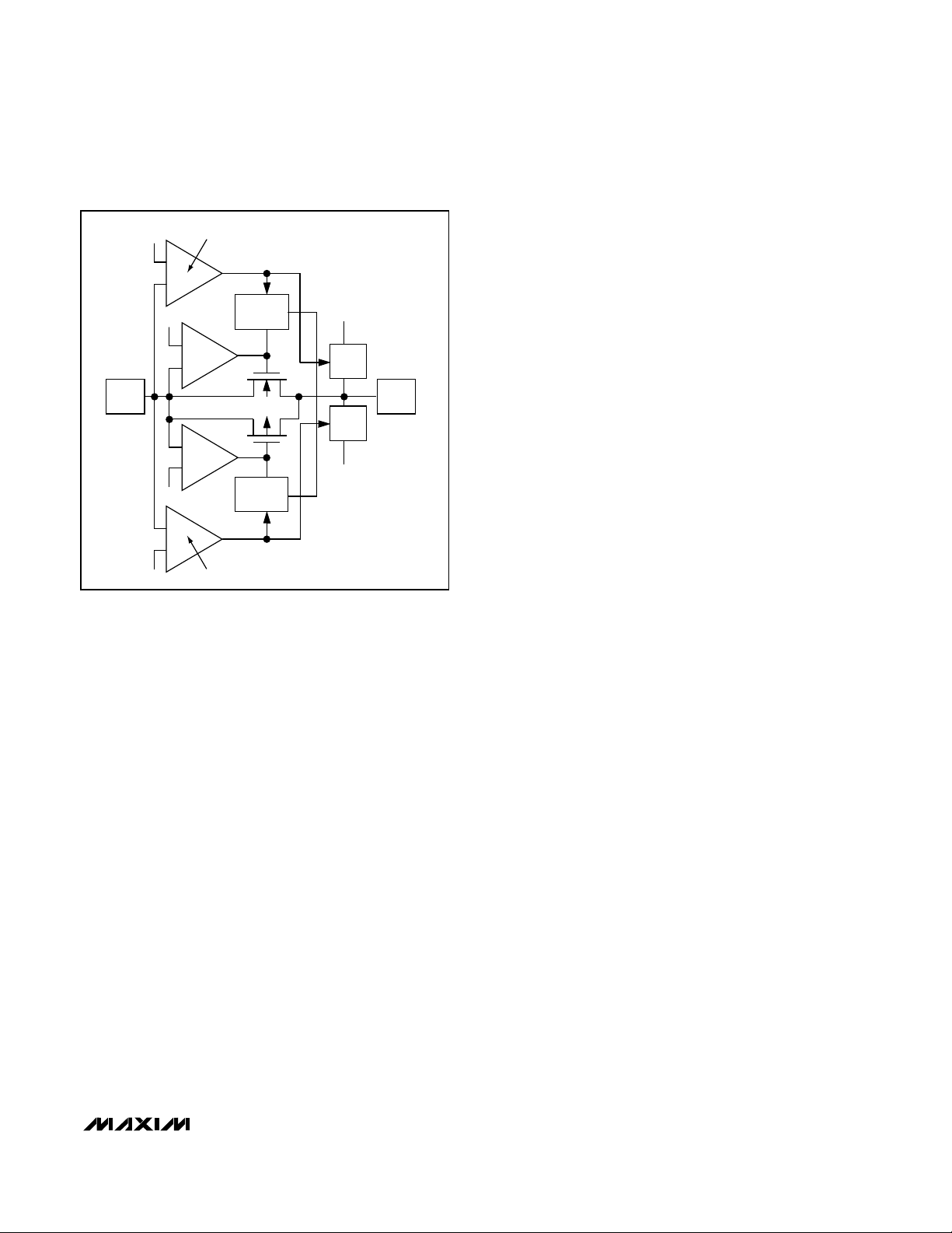
The MAX4631/MAX4632/MAX4633 are fault-protected
analog switches with special operation and construction. Traditional fault-protected switches are constructed using three series CMOS devices. This combination
produces good fault-protection but fairly high on-resistance when the signals are within 3V of each supply
rail. These series devices are not capable of handling
signals up to the power-supply rails.
These devices differ considerably from traditional faultprotection switches, with three advantages. First, they
are constructed with two parallel FETs, allowing very low
on-resistance when the switch is on. Second, they allow
signals on the NC_ or NO_ pins that are within or slightly
beyond the supply rails to be passed through the switch
to the COM_ terminal, allowing rail-to-rail signal operation. Third, when a signal on NC_ or NO_ exceeds the
supply rails by about 50mV (a fault condition), the voltage on COM_ is limited to the appropriate polarity supply voltage. Operation is identical for both fault
polarities. The fault-protection extends to ±25V
(MAX4632) or ±36V (MAX4631/MAX4633) with power
on and ±40V with power off.
The MAX4631/MAX4632/MAX4633 have a parallel Nchannel and P-channel MOSFET switch configuration with
input voltage sensors. The simplified structure is shown
in Figure 1. The parallel N1 and P1 MOSFETs form the
switch element. N3 and P3 are sensor elements to sample the input voltage and compare it against the powersupply rails.
During normal operation of a conducting channel, N1
and P1 remain on with a typical 62Ω on-resistance
between NO_ (or NC_) and COM_. If the input voltage
exceeds either supply rail by about 50mV, the parallel
combination switches (N1, P1) are forced off through
the driver and sensing circuitry. At the same time, the
output (COM_) is clamped to the appropriate supply
rail by the clamp circuitry (N2, P2). Two clamp circuits
limit the output voltage to the supply voltages.
Pin Compatibility
These switches have identical pinouts to common nonfault-protected CMOS switches (DG401, DG403,
DG405). Exercise care in considering them as direct
replacements in existing printed circuit boards, since
only the NO_ and NC_ pins of each switch are fault protected.
Normal Operation
Two comparators continuously compare the voltage on
the NO_ (or NC_) pin with V+ and V- supply voltages
(Figure 1). When the signal on NO_ (or NC_) is between
V+ and V-, the switch behaves normally, with FETs N1
and P1 turning on and off in response to NO_ (or NC_)
signals.
For any voltage between the supply rails, the switch is
bidirectional; therefore, COM_ and NO_ (or NC_) are
interchangeable. Only NO_ and NC_ can be exposed
to overvoltages beyond the supply range and within the
specified breakdown limits of the device.
Fault Condition
The MAX4631/MAX4632/MAX4633 protect devices
connected to their outputs (COM_) through their unique
fault-protection circuitry. When the input voltage is
raised 50mV above either supply rail, the internal sense
and comparator circuitry (N3 and N-channel driver or
P3 and P-channel driver) disconnect the output (COM_)
from the input (Figure 1).
If the switch driven above the supply rail has an on
state, the clamp circuitry (N2 or P2) connects the output to the appropriate supply rail. Table 1 summarizes
the switches’ operation under normal and fault conditions.
Figure 1. Simplified Internal Structure
-15V
-15V
NC_
or
INPUT
NO_
+15V
+15V
N3
SENSE
SWITCH
SENSE
SWITCH
COMPARATOR
N-CHANNEL
DRIVER
P3
P-CHANNEL
DRIVER
COMPARATOR
-V (-15V)
N2
CLAMP
N1
P1
CLAMP
+V (+15V)
OUTPUT COM_
P2
Page 10
MAX4631/MAX4632/MAX4633
Fault-Protected, High-Voltage,
Dual Analog Switches
10 ______________________________________________________________________________________
Transient Fault Response and Recovery
When a fast rising and falling transient on NO_ (or NC_)
exceeds V+ or V-, the output (COM_) follows the input
(IN_) to the supply rail with only a few nanoseconds of
delay. This delay is due to the switch on-resistance and
circuit capacitance to ground. However, when the input
transient returns to within the supply rails, there is a
longer output recovery time delay. For positive and
negative faults, the recovery time is typically 2.5µs.
These values depend on the COM_ output resistance
and capacitance, and are not production tested or
guaranteed. The delays are not dependent on the fault
amplitude. Higher COM_ output resistance and capacitance increase recovery times.
Fault-Protection Voltage and Power Off
The maximum fault voltage on the NO_ (or NC_) pins is
±40V when the power is off. For the MAX4631/
MAX4633, with ±15V supplies, the highest voltage on
NO_ (or NC_) can be +36V, and the lowest voltage on
NO (or NC_) can be -36V. For the MAX4632, with ±15V
supplies, the highest voltage on NO_ (or NC_) can be
+25V, and the lowest voltage on NO_ (or NC_) can be
-25V. Exceeding these limits can damage the device.
IN_ Logic-Level Thresholds
The logic-level thresholds are TTL/CMOS compatible
when V+ is +15V. Raising V+ increases the threshold
slightly; when V+ reaches +25V, the level threshold is
about 2.8V—higher than the TTL output high-level minimum of 2.4V, but still compatible with CMOS outputs
(see
Typical Operating Characteristics
).
Increasing V- has no effect on the logic-level thresholds, but it does increase the gate-drive voltage to the
signal FETs, reducing their on-resistance.
Failure Modes
The MAX4631/MAX4632/MAX4633 are not lightning
arrestors or surge protectors. Exceeding the fault-protection voltage limits on NO_ or NC_, even for very short
periods, can cause the device to fail. The failure modes
may not be obvious, and failure in one switch may or
may not affect other switches in the same package.
__________Applications Information
Ground
There is no connection between the analog signal
paths and GND. The analog signal paths consist of an
N-channel and a P-channel MOSFET with their sources
and drains paralleled and their gates driven out of
phase to V+ and V- by the logic-level translators.
V+ and GND power the internal logic and logic-level
translators and set the input logic thresholds. The logiclevel translators convert the logic levels to switched V+
and V- signals to drive the analog switch gates. This
drive signal is the only connection between the power
supplies and the analog signals. GND, IN_, and COM_
have ESD-protection diodes to V+ and V-.
Supply-Current Reduction
When the logic signals are driven rail-to-rail from 0 to
+12V or -15V to +15V, the supply current reduces to
approximately half of the supply current when the logic
input levels are at 0 to +5V.
Power Supplies
The MAX4631/MAX4632/MAX4633 operate with bipolar
supplies between ±4.5V and ±18V. The V+ and V- supplies need not be symmetrical, but their difference can
not exceed the absolute maximum rating of +44V.
These devices operate from a single supply between
+9V and +36V when V- is connected to GND.
INPUT
RANGE
On Between Rails
POWER
SUPPLIES
(V+, V-)
NC_
On
NO_
Off
OUTPUT
NC_
On Between Rails Off On NO_
On Between V+ and (+40V - V+) On Off V+
On Between V+ and (+40V - V+) Off On V+
On Between V- and (-40V - V-) On Off VOn Between V+ and (-40V - V-) Off On V-
Off Between Rails Off Off
Follows the load
terminal voltage
Table 1. Switch States in Normal and Fault Conditions
Page 11

MAX4631/MAX4632/MAX4633
Fault-Protected, High-Voltage,
Dual Analog Switches
______________________________________________________________________________________ 11
High-Frequency Performance
In 50Ω systems, signal response is reasonably flat up
to 30MHz (see
Typical Operating Characteristics
).
Above 30MHz, the on-response has several minor
peaks that are highly layout dependent. The problem
with high-frequency operation is not turning the switch
on, but turning it off. The off-state switch acts like a
capacitor and passes higher frequencies with less
attenuation. At 10MHz, off-isolation is about -46dB in
50Ω systems, declining (approximately 20dB per
decade) as frequency increases. Higher circuit impedance also diminishes off-isolation. Adjacent channel
attenuation is about 3dB above that of a bare IC socket
and is due entirely to capacitive coupling.
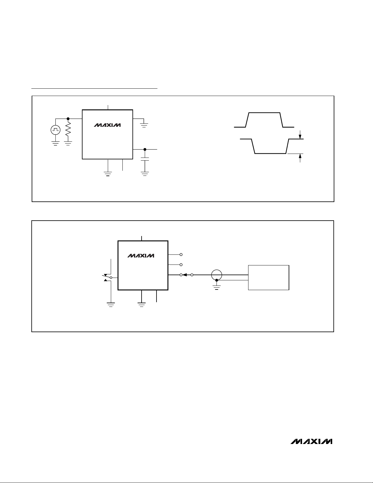
Test Circuits/Timing Diagrams
Figure 3. MAX4631 Break-Before-Make Interval
Figure 2. Switch Turn-On/Turn-Off Times
V- IS CONNECTED TO GND (0V) FOR SINGLE-SUPPLY OPERATION.
V+
V+
NO_ OR NC_
MAX4631
V
IN_
50Ω
IN_
MAX4632
MAX4633
GND
COM_
V-
V-
+10V
R
L
10pF
V
OUT
V+
V
IN_
0V
+10V
V
OUT
0V
t
OFF
50% 50%
90%
90%
t
ON
V+
V
IN_
IN_
IN_
50Ω
V- IS CONNECTED TO GND (0V) FOR SINGLE-SUPPLY OPERATION.
V+
MAX4631
GND V-
COM_
COM_
V-
NO_
NC_
R
L
+10V
10pF
< 5ns
t
V+
V
IN_
0V
, V
V
NO_
NC_
V
OUT
V
OUT
0V
50% 50%
80%
t
OPEN
R
t
F
< 5ns
Page 12
MAX4631/MAX4632/MAX4633
Fault-Protected, High-Voltage,
Dual Analog Switches
12 ______________________________________________________________________________________
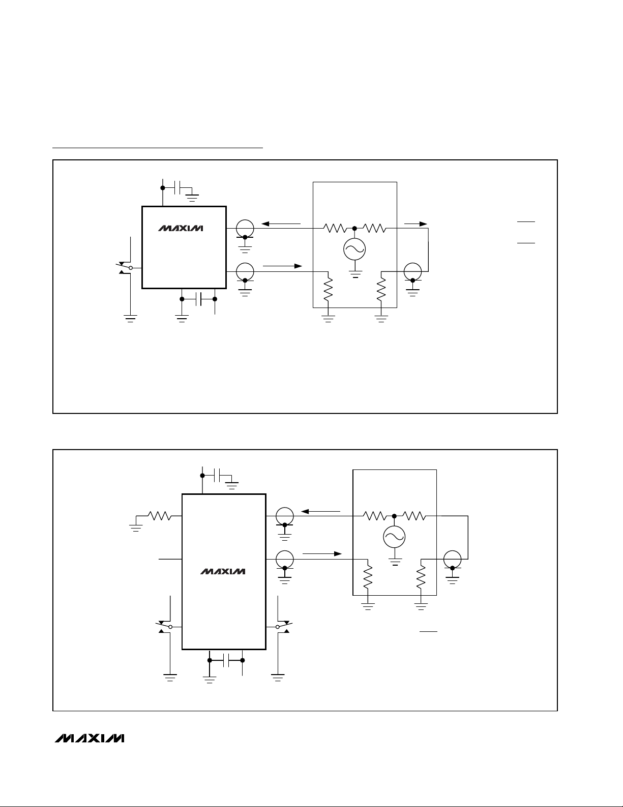
Figure 4. Charge Injection
Figure 5. COM_, NO_, and NC_ Capacitance
Test Circuits/Timing Diagrams (continued)
V+
V
IN_
IN_
50Ω
V+
NO_ OR NC_
MAX4631
MAX4632
MAX4633
GND
COM_
V-
C
L
100pF
V
IN_
V
V
OUT
OUT
V+
0V
∆ V
OUT
V-
V- IS CONNECTED TO GND (0V) FOR SINGLE-SUPPLY OPERATION. Q = ∆ V
V+
V+
V+
MAX4631
MAX4632
V- IS CONNECTED TO GND (0V) FOR SINGLE-SUPPLY OPERATION.
ADDRESS SELECT
IN_
MAX4633
GND
NO_
NC_
COM_
V-
V-
∆ V
IS THE MEASURED VOLTAGE DUE TO CHARGE-
OUT
TRANSFER ERROR Q WHEN THE CHANNEL TURNS OFF.
• C
OUT
L
1MHz
CAPACITANCE
ANALYZER
Page 13
MAX4631/MAX4632/MAX4633
Fault-Protected, High-Voltage,
Dual Analog Switches
______________________________________________________________________________________ 13
Figure 6. Frequency Response and Off-Isolation
Figure 7. Crosstalk
Test Circuits/Timing Diagrams (continued)
10nF
V+
V+
COM_
MAX4631
MAX4632
MAX4633
ADDRESS SELECT
MEASUREMENTS ARE STANDARDIZED AGAINST SHORT AT SOCKET TERMINALS.
OFF-ISOLATION IS MEASURED BETWEEN COM_ AND “OFF” NO_ OR NC_ TERMINALS.
ON LOSS IS MEASURED BETWEEN COM_ AND “ON” NO_ OR NC_ TERMINALS.
SIGNAL DIRECTION THROUGH SWITCH IS REVERSED; WORST VALUES ARE RECORDED.
V- IS CONNECTED TO GND (0V) FOR SINGLE-SUPPLY OPERATION.
IN_
GND
NO_, NC_
10nF
V-
V-
NETWORK
ANALYZER
V
IN
V
OUT
50Ω
MEAS. REF.
50Ω 50Ω
50Ω
OFF-ISOLATION = 20 log
ON-LOSS = 20 log
V
OUT
V
IN
V
OUT
V
IN
V- IS CONNECTED TO GND (0V) FOR SINGLE-SUPPLY OPERATION.
10nF
V+
NETWORK
ANALYZER
50Ω
NO_, NC_ COM_
NO_, NC_COM_
MAX4631
2.4V 2.4V
MAX4632
MAX4633
IN1 IN2
10nF
V-
V-
GND
V
IN
V
OUT
50Ω
MEAS. REF.
50Ω 50Ω
CROSSTALK = 20 log
50Ω
V
OUT
V
IN
Page 14

MAX4631/MAX4632/MAX4633
Fault-Protected, High-Voltage,
Dual Analog Switches
14 ______________________________________________________________________________________
Pin Configurations/Functional Diagrams/Truth Tables
Chip Information
TRANSISTOR COUNT: 223
TOP VIEW
COM1
N.C.
N.C.
N.C.
N.C.
N.C.
N.C.
COM2
1
2
3
4
5
MAX4631
6
7
8
DIP/SO
MAX4631
LOGIC SWITCH
0
1
OFF
NO1
16
IN1
15
V-
14
GND
13
N.C.
12
V+
11
IN2
10
NO2
9
COM1
N.C.
COM3
NC3
NC4
COM4
N.C.
COM2
1
2
3
4
5
6
7
8
MAX4632
NO1
16
IN1
15
V-
14
GND
13
N.C.
12
V+
11
IN2
10
NO2
9
DIP/SO
LOGIC
0
ON
1
SWITCHES SHOWN FOR LOGIC "0" INPUT N.C. = NOT INTERNALLY CONNECTED
MAX4632
SWITCHES 1, 2
OFF
ON
SWITCHES 3, 4
ON
OFF
COM1
N.C.
COM3
NO3
NO4
COM4
N.C.
COM2
1
2
3
4
5
6
7
8
MAX4633
DIP/SO
MAX4633
LOGIC SWITCH
0
1
OFF
ON
NO1
16
IN1
15
V-
14
GND
13
N.C.
12
V+
11
IN2
10
NO2
9
Page 15

MAX4631/MAX4632/MAX4633
Fault-Protected, High-Voltage,
Dual Analog Switches
______________________________________________________________________________________ 15
Package Information
SOICN.EPS
Page 16

MAX4631/MAX4632/MAX4633
Fault-Protected, High-Voltage,
Dual Analog Switches
Maxim cannot assume responsibility for use of any circuitry other than circuitry entirely embodied in a Maxim product. No circuit patent licenses are
implied. Maxim reserves the right to change the circuitry and specifications without notice at any time.
16
____________________Maxim Integrated Products, 120 San Gabriel Drive, Sunnyvale, CA 94086 408-737-7600
© 1999 Maxim Integrated Products Printed USA is a registered trademark of Maxim Integrated Products.
MAX4631/MAX4632/MAX4633
Package Information (continued)
PDIPN.EPS
 Loading...