

For free samples & the latest literature: http://www.maxim-ic.com, or phone 1-800-998-8800.
For small orders, phone 1-800-835-8769.
General Description
The MAX4626/MAX4627/MAX4628 are low-on-resistance, low-voltage, single-pole/single-throw (SPST)
analog switches that operate from a +1.8V to +5.5V single supply. The MAX4626 is normally open (NO), and
the MAX4627 is normally closed (NC). The MAX4628 is
normally open (NO) and has two control inputs. These
devices also have fast switching speeds (tON= 50ns
max, t
OFF
= 30ns max).
When powered from a +5V supply, the MAX4626/
MAX4627/MAX4628 offer 0.5Ω max on-resistance
(RON) with 0.1Ω max RONflatness, and their digital
logic inputs are TTL compatible. These switches also
feature overcurrent protection to prevent device damage from short circuits and excessive loads.
The MAX4626 is pin compatible with the MAX4514, and
the MAX4627 is pin compatible with the MAX4515. The
MAX4626/MAX4627 are available in SOT23-5 packages; the MAX4628 is available in a SOT23-6 package.
Applications
Power Routing
Battery-Operated Equipment
Audio and Video Signal Routing
Low-Voltage Data-Acquisition Systems
Communications Circuits
PCMCIA Cards
Cellular Phones
Modems
Hard Drives
Features
♦ Low R
ON
0.5Ω max (+5V Supply)
0.9Ω max (+3V Supply)
♦ 0.1Ω max RONFlatness (+5V Supply)
♦ Overcurrent Protection
♦ Single-Supply Operation (+1.8V to +5.5V)
♦ Available in SOT23 Packages
♦ Fast Switching: t
ON
= 50ns max, t
OFF
= 30ns max
♦ TTL-Logic Compatible at +5V
♦ Pin Compatible with MAX4514 (MAX4626)
Pin Compatible with MAX4515 (MAX4627)
MAX4626/MAX4627/MAX4628
0.5Ω, Low-Voltage, Single-Supply
SPST Analog Switches
________________________________________________________________ Maxim Integrated Products 1
19-1633; Rev 0; 1/00
PART
MAX4626EUK-T
MAX4627EUK-T
-40°C to +85°C
-40°C to +85°C
TEMP. RANGE
PIN-
PACKAGE
5 SOT23-5
5 SOT23-5
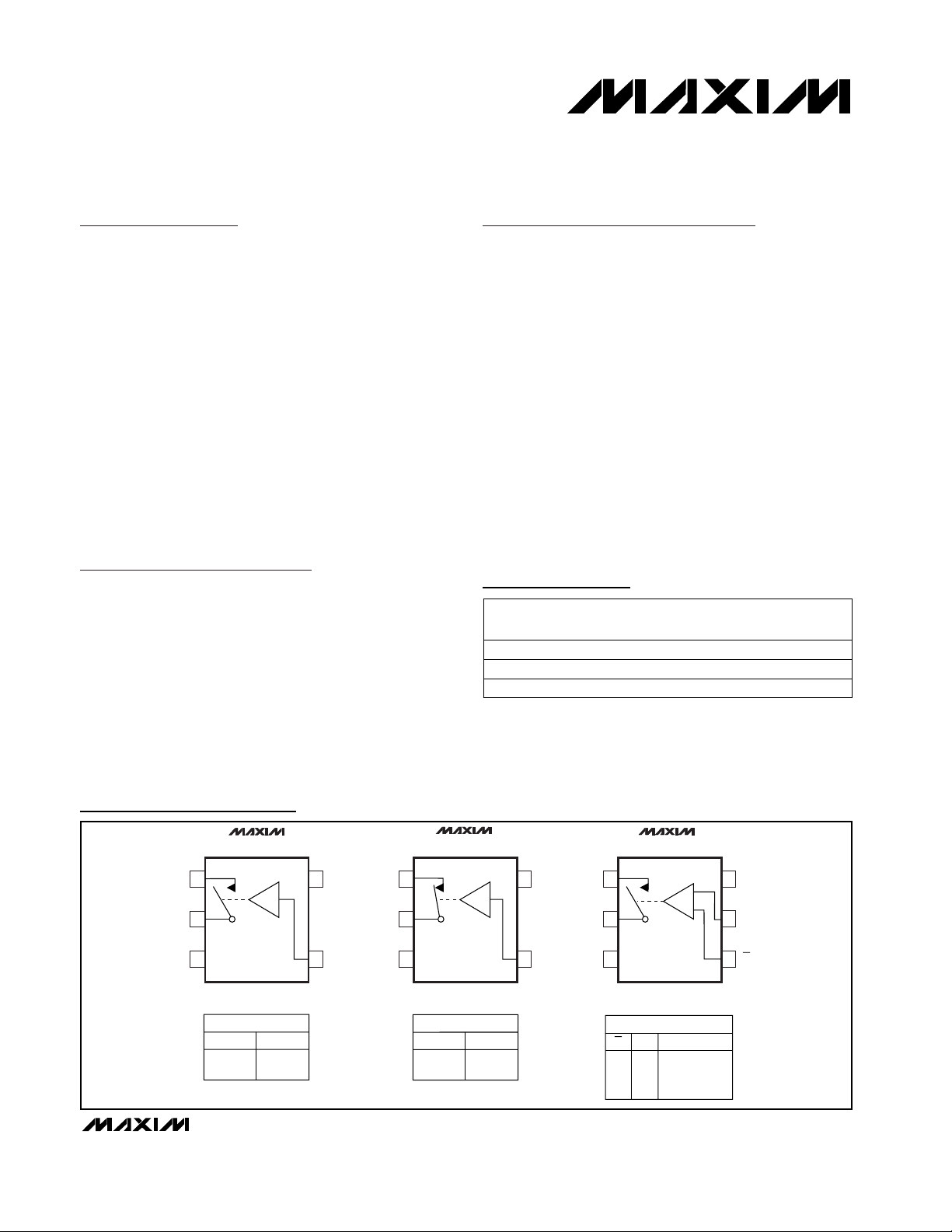
Pin Configurations/Functional Diagrams/Truth Tables
Ordering Information
TOP
MARK
ADMJ
ADMK
MAX4628EUT-T
-40°C to +85°C AADN6 SOT23-6
TOP VIEW
GND
MAX4626
15V+COM
NO
2
3
SOT23-5
MAX4626
LOGIC
0
1
SWITCH
OFF
ON
MAX4627
15
COM
NC
2
SWITCH
ON
OFF
4
4
IN
3
GND
SOT23-5
MAX4627
LOGIC
0
1
SWITCHES SHOWN FOR LOGIC "0" INPUT.
COM
V+
NO
GND
IN
MAX4628
1
2
3
SOT23-6
MAX4628
SWITCH
IN
IN
1
0
1
1
0
0
0
1
OFF
OFF
OFF
6 V+
5 IN
4
IN
ON
MAX4626/MAX4627/MAX4628
0.5Ω, Low-Voltage, Single-Supply
SPST Analog Switches
2 _______________________________________________________________________________________
ABSOLUTE MAXIMUM RATINGS
ELECTRICAL CHARACTERISTICS—Single +5V Supply
(V+ = +5V ±10%, GND = 0, V
INH
= 2.4V, V
INL
= 0.8V, TA= T
MIN
to T
MAX
, unless otherwise noted.) (Notes 2, 3)
Stresses beyond those listed under “Absolute Maximum Ratings” may cause permanent damage to the device. These are stress ratings only, and functional
operation of the device at these or any other conditions beyond those indicated in the operational sections of the specifications is not implied. Exposure to
absolute maximum rating conditions for extended periods may affect device reliability.
Voltages Referenced to GND
V+, IN, IN..................................................................-0.3V to +6V
NO, NC, COM (Note 1).................................-0.3V to (V+ + 0.3V)
Continuous Current NO, NC to COM .............................±400mA
Peak Switch Current NO, NC to COM
(pulsed at 1ms, 10% duty cycle max) ........................ ±800mA
Continuous Power Dissipation (T
A
= 70°C)
5-Pin SOT23-5 (derate 7.1mW/°C above +70°C) ..........571mW
6-Pin SOT23-6 (derate 7.1mW/°C above +70°C) ..........571mW
Operating Temperature Range
MAX462_EU_....................................................-40°C to +85°C
Junction Temperature......................................................+150°C
Storage Temperature Range .............................-65°C to +150°C
Lead Temperature (soldering, 10s) ................................ +300°C
Note 1: Signals on NC, NO, or COM exceeding V+ or GND are clamped by internal diodes.
PARAMETER SYMBOL MIN TYP MAX UNITS
Analog Signal Range
V
COM
, VNO,
V
NC
0V+V
0.35 0.5
On-Resistance R
ON
TA= +25°C
0.6
Ω
0.05 0.10
On-Resistance Flatness
(Note 4)
R
FLAT(ON)
V+ = 4.5V; V
COM
= 0, 1V,
2V; I
COM
= 100mA
TA= +25°C
0.10
Ω
-2 0.2 2
NO or NC Off-Leakage
Current
I
NO(OFF)
,
I
NC(OFF)
TA= +25°C
-20 20
nA
-2 0.2 2
COM Off-Leakage
Current
I
COM(OFF)
TA= +25°C
-20 20
nA
COM On-Leakage
Current
-4 0.3 4
I
COM(ON)
TA= +25°C
-40 40
nA
Overcurrent-Protection
Threshold Current
TA= +25°C 2.4 A
TA= +25°C 40 50
Turn-On Time t
ON
VNOor VNC= 3V, Figure 2
TA= T
MIN
to T
MAX
60
ns
TA= +25°C 18 30
Turn-Off Time t
OFF
VNOor VNC= 3V, Figure 2
TA= T
MIN
to T
MAX
40
ns
TA= T
MIN
to T
MAX
TA= T
MIN
to T
MAX
TA= T
MIN
to T
MAX
TA= T
MIN
to T
MAX
CONDITIONS
TA= T
MIN
to T
MAX
V+ = 5.5V; V
COM
= 1V, 4.5V;
VNOor VNC= 4.5V, 1V
V+ = 5.5V; V
COM
= 1V, 4.5V;
V
NO
or VNC= 4.5V, 1V
V+ = 5.5V; V
COM
= 1V, 4.5V;
V
NO
or VNC= 1V, 4.5V, or
floating
V+ = 4.5V,
VNOor VNC= 3.5V,
I
COM
= 100mA
Charge Injection Q CL= 1.0nF, V
GEN
= 0, R
GEN
= 0, TA= +25°C, Figure 3 40 pC
Off-Isolation (Note 5) OIRR RL= 50Ω, CL= 5pF, f = 1MHz, TA= +25°C, Figure 4 -51 dB
COM Off-Capacitance C
COM(OFF)
f = 1MHz, TA= +25°C, Figure 5 65 pF
COM On-Capacitance C
COM(ON)
f = 1MHz, TA= +25°C, Figure 5 130 pF
NC or NO OffCapacitance
C
OFF
f = 1MHz, TA= +25°C, Figure 5 65 pF
DYNAMIC
ANALOG SWITCH
MAX4626/MAX4627/MAX4628
0.5Ω, Low-Voltage, Single-Supply
SPST Analog Switches
_______________________________________________________________________________________ 3
ELECTRICAL CHARACTERISTICS—Single +3V Supply
(V+ = +2.7V to +3.6V, GND = 0, V
INH
= 2.0V, V
INL
= 0.6V, TA= T
MIN
to T
MAX
, unless otherwise noted.) (Notes 2, 3)
V0V+
V
COM
, VNO,
V
NC
Analog Signal Range
CONDITIONS UNITSMIN TYP MAXSYMBOLPARAMETER
V2.0V
INH
Input Voltage High
µA-1 1I
IN
Logic Input Current
ELECTRICAL CHARACTERISTICS—Single +5V Supply (continued)
(V+ = +5V ±10%, GND = 0, V
INH
= 2.4V, V
INL
= 0.8V, TA= T
MIN
to T
MAX
, unless otherwise noted.) (Notes 2, 3)
0.9
Ω
0.4 0.8
V+ = 2.7V,
VNOor VNC= 1.5V,
I
COM
= 100mA
R
ON
On-Resistance
TA= +25°C
TA= T
MIN
to T
MAX
0.1 ΩR
FLAT(ON)
On-Resistance Flatness
(Note 4)
V+ = 2.7V; I
COM
= 100mA;
V
NO
or VNC= 0, 0.75V, 1.5V; TA= +25°C
ns
65 80
VNOor V
NC
= 1.5V,
Figure 2
t
ON
Turn-On Time
90
ns
22 40
VNOor V
NC
= 1.5V,
Figure 2
t
OFF
Turn-Off Time
50TA= T
MIN
to T
MAX
TA= +25°C
TA= T
MIN
to T
MAX
TA= +25°C
µA10V+ = 5.5V, VIN= 0 or V+I+Positive Supply Current
V1.8 5.5V+Power-Supply Range
µA-1 1I
IN
Logic Input Current
V2.4V
INH
Input Voltage High
V0.8V
INL
Input Voltage Low
CONDITIONS UNITSMIN TYP MAXSYMBOLPARAMETER
LOGIC INPUT
SUPPLY
Note 2: The algebraic convention, where the most negative value is a minimum and the most positive value a maximum, is used in
this data sheet.
Note 3: SOT-packaged parts are 100% tested at +25°C. Limits across the full temperature range are guaranteed by design and
correlation.
Note 4: Flatness is defined as the difference between the maximum and minimum values of on-resistance as measured over the
specified analog signal range.
Note 5: Off-Isolation = 20log
10[VCOM
/ (VNCor VNO)], V
COM
= output, VNCor VNO= input to off switch.
pC
30
CL= 1.0nF, Figure 3, V
GEN
= 0, R
GEN
= 0,
Ta = +25°C
QCharge Injection
V0.6V
INL
Input Voltage Low
µA10V = +3.6V, VIN= 0I+Positive Supply Current
ANALOG SWITCH
DYNAMIC
LOGIC INPUT
SUPPLY
t
OFF
t
ON
0
20
40
80
60
100
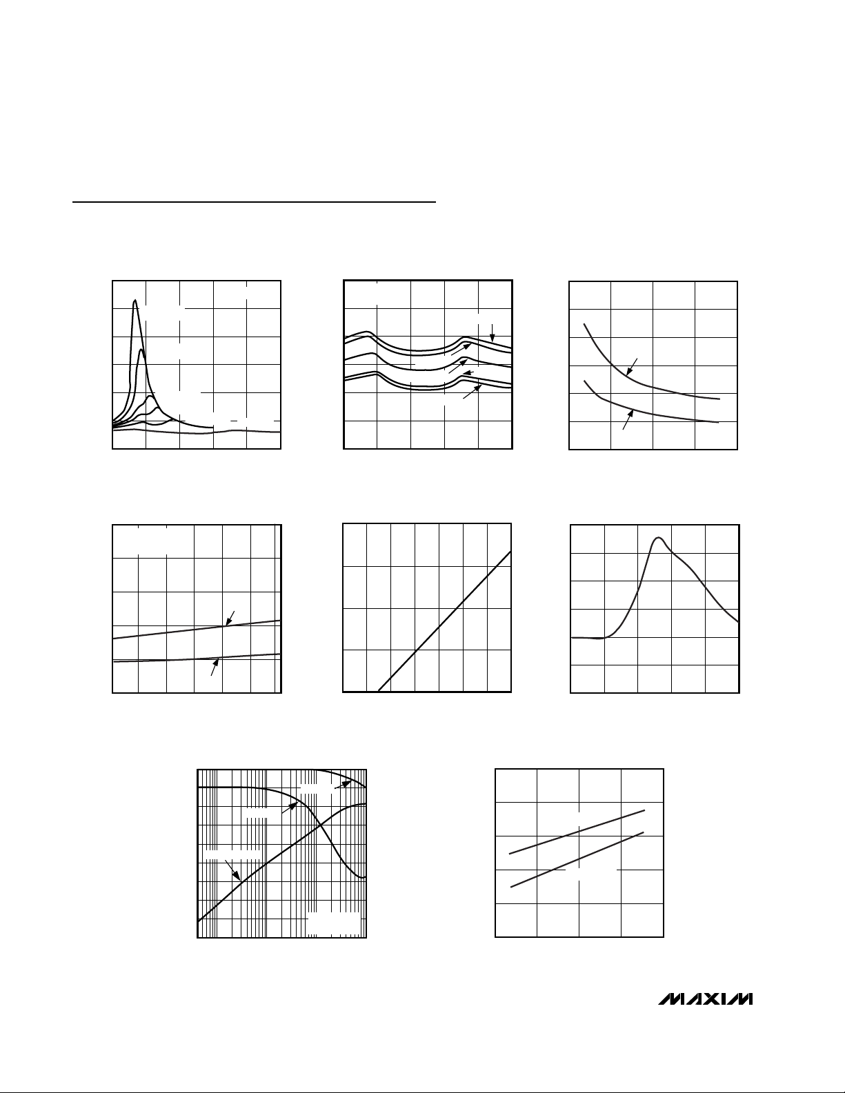
-40 0-20 20 6040 80
TURN-ON/OFF TIMES
vs. TEMPERATURE
MAX4626/7/8-04
TEMPERATURE (°C)
t
ON/
t
OFF
(ns)
V+ = 5V
V
NO
or VNC = 3V
0.001
0.01
0.1
1
10
ON/OFF-LEAKAGE CURRENT
vs. TEMPERATURE
MAX4626/7/805
TEMPERATURE (°C)
ON/OFF-LEAKAGE (nA)
-40 20 40-20 0 60 80 100
0
20
60
40
100
80
120
012345
CHARGE INJECTION vs. COM VOLTAGE
MAX4626/7/8-06
V
COM
(V)
Q (pC)
0
-90
30k 100k 1M
10M
100M
FREQUENCY RESPONSE
-80
MAX4626/7/8-07
FREQUENCY (Hz)
LOSS (dB)
PHASE (degrees)
-30
-40
-50
-60
-70
-20
-10
V+ = 5V
50Ω = IN/OUT
OFF-ISOLATION
ON-LOSS
ON-PHASE
10
0
-10
-20
-30
-40
-50
-60
-70
-80
0
0.5
1.0
2.0
1.5
2.5
234 5 6
LOGIC THRESHOLD VOLTAGE
vs. SUPPLY VOLTAGE
MAX4626/7/8-08
SUPPLY VOLTAGE (V)
LOGIC THRESHOLD VOLTAGE (V)
VIN RISING
VIN FALLING
MAX4626/MAX4627/MAX4628
0.5Ω, Low-Voltage, Single-Supply
SPST Analog Switches
4 _______________________________________________________________________________________
Typical Operating Characteristics
(TA = +25°C, unless otherwise noted.)
0
1.0
0.5
2.0
1.5
2.5
3.0
021 345
ON-RESISTANCE vs. COM VOLTAGE
OVER SUPPLY VOLTAGE
MAX4626/7/801
V
COM
(V)
R
ON
(Ω)
I
COM
= 100mA
V
CC =
+1.8V
V
CC =
+2.0V
V
CC =
+2.3V
V
CC =
+2.5V
V
CC =
+3.0V
V
CC =
+5V
0
0.2
0.1
0.4
0.3
0.5
0.6
021 345
ON-RESISTANCE vs. COM VOLTAGE
OVER TEMPERATURE
MAX4626/7/8-02
V
COM
(V)
R
ON
(Ω)
V + = 5V
I
COM
= 100mA
TA = +85°C
TA = -40°C
TA = -55°C
TA = +25°C
TA = +105°C
TURN-ON/OFF TIMES
vs. SUPPLY VOLTAGE
0
10
30
20
50
40
60
23456
MAX4626/7/8-03
V
SUPPLY
(V)
t
ON/
t
OFF
(ns)
t
OFF
t
ON
MAX4626/MAX4627/MAX4628
0.5Ω, Low-Voltage, Single-Supply
SPST Analog Switches
_______________________________________________________________________________________ 5
Typical Operating Characteristics (continued)
(TA = +25°C, unless otherwise noted.)
Pin Description
1
2
3
4
—
5
MAX4626
—
1
—
3
4
2
5
MAX4627
—
MAX4628
4
IN
Inverted Digital Control Input (see MAX4628 Truth Table)
NAME FUNCTION
1
COM Analog Switch—Common
2 NO Analog Switch—Normally Open
3 GND Ground
5 IN Digital Control Input
— NC Analog Switch—Normally Closed
6 V+ Positive Supply Input
PIN
TOTAL HARMONIC DISTORTION
vs. FREQUENCY
FREQUENCY (Hz)
0.1
0.01
THD (%)
0.001
10 1k100 10k 100k
OVERCURRENT RESPONSE
3V
V
COM
2V/div
MAX4626/7/8-09
0
3A
0
500µs/div
MAX4626/7/810
I
COM
1A/div

MAX4626/MAX4627/MAX4628
0.5Ω, Low-Voltage, Single-Supply
SPST Analog Switches
6 _______________________________________________________________________________________
Detailed Description
The MAX4626/MAX4627/MAX4628 are low-on-resistance (RON), low-voltage, single-pole/single-throw
(SPST) analog switches that operate from a +1.8V to
+5.5V single supply. The MAX4626 is normally open
(NO), and the MAX4627 is normally closed (NC). The
MAX4628 is normally open (NO) and has two control
inputs.
When powered from a +5V supply, their 0.5Ω R
ON
allows high continuous currents to be switched in a
variety of applications. In the event of an overcurrent
condition, these switches provide both current-limit and
thermal-shutdown protection.
Current-Limit Protection
The MAX4626/MAX4627/MAX4628 feature current-limit
protection circuitry. When the voltage drop across the
on switch reaches 0.6V (typ), the internal circuitry activates. The current limit is not instantaneous, but rather
integrates over time so that current limiting will not activate under momentary short-circuit conditions encountered when the switch output charges a small 0.1µF
capacitor. For sustained overcurrent conditions, the
switch turns off (opens). The switch turns on after 5ms
and, if the overload condition persists, the switch will
cycle off and on to produce a pulsed output. A direct
short circuit will be detected immediately, and the
switch will pulse on for 1µs, then remain off for 5ms.
Applications Information
Logic Inputs
The MAX4626/MAX4627/MAX4628 logic inputs can be
driven up to +5.5V regardless of the supply voltage. For
example, with a +3.3V supply, IN or IN may be driven
low to 0V and high to 5.5V. Driving IN or IN Rail-to-Rail
®
minimizes power consumption.
Analog Signal Levels
Analog signals that range over the entire supply voltage
(V+ to GND) can be passed with very little change in
on-resistance (see Typical Operating Characteristics).
The switches are bidirectional, so the NO, NC, and
COM pins can be used as either inputs or outputs.
Power-Supply Sequencing and
Overvoltage Protection
Caution: Do not exceed the absolute maximum ratings; stresses beyond the listed ratings may cause
permanent damage to the devices.
Proper power-supply sequencing is recommended for
all CMOS devices. Always apply V+ before applying
analog signals, especially if the analog signal is not
current limited. If this sequencing is not possible, and if
the analog inputs are not current limited to <20mA, add
a small-signal diode (D1) as shown in Figure 1. If the
analog signal can dip below GND, add D2. Adding
protection diodes reduces the analog range to a diode
drop (about 0.7V) below V+ (for D1), and a diode drop
above ground (for D2). On-resistance increases by a
small amount at low supply voltages. Maximum supply
voltage (V+) must not exceed +6V.
Adding protection diode D2 causes the logic thresholds to be shifted relative to GND. TTL compatibility is
not guaranteed when protection diode D2 is added.
Protection diodes D1 and D2 also protect against some
overvoltage situations. With Figure 1’s circuit, if the supply voltage is below the absolute maximum rating, and
if a fault voltage up to the absolute maximum rating is
applied to an analog signal pin, no damage will result.
Figure 1. Overvoltage Protection Using Two External Blocking
Diodes
Rail-to-Rail is a registered trademark of Nippon Motorola, Ltd.
POSITIVE SUPPLY
D1
V+
NO
V
g
COM
MAX4626
MAX4627
MAX4628
GND
D2
MAX4626/MAX4627/MAX4628
0.5Ω, Low-Voltage, Single-Supply
SPST Analog Switches
_______________________________________________________________________________________ 7
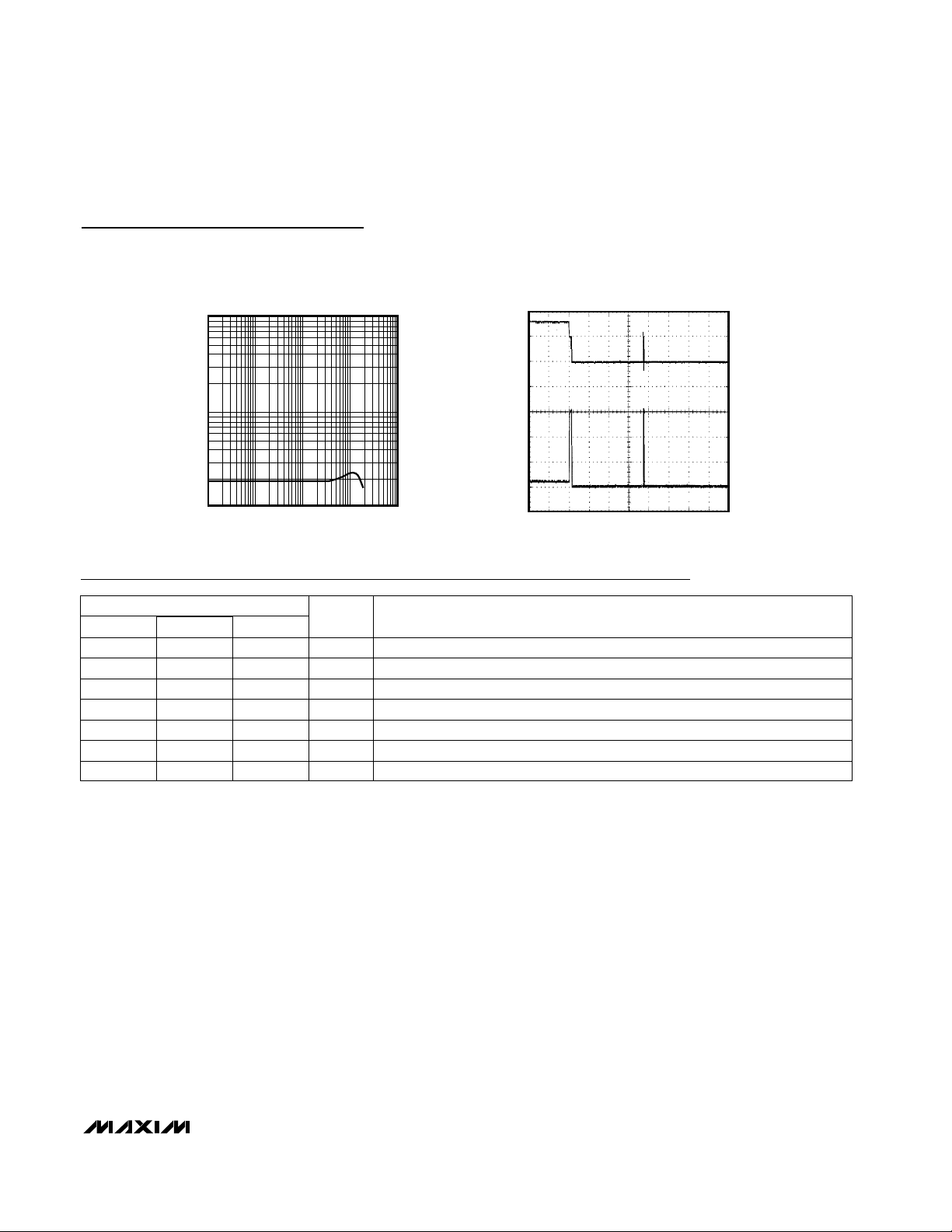
Figure 2. Switching Time
Test Circuits/Timing Diagrams
Figure 3. Charge Injection
Figure 4. On-Loss and Off-Isolation
MAX4626
MAX4627
MAX4628
V
N_
LOGIC
INPUT
CL INCLUDES FIXTURE AND STRAY CAPACITANCE.
V
OUT
RL + R
MAX4626
MAX4627
MAX4628
V
GEN
R
GEN
NO
OR NC
IN
GND
= V
N_ (
NC
OR NO
GND
R
L
V+
V+
COM
R
L
50Ω
)
ON
V+
V+
COM
IN
V
OUT
C
L
35pF
V
OUT
C
L
LOGIC
INPUT
SWITCH
OUTPUT
V
OUT
IN
V
INH
V
INL
0V
OFF
50%
V
OUT
0.9 · V
0UT
t
ON
LOGIC INPUT WAVEFORMS INVERTED FOR SWITCHES
THAT HAVE THE OPPOSITE LOGIC SENSE.
ON
tr < 5ns
tf < 5ns
t
OFF
0.9 · V
OUT
∆V
OUT
OFF
0V OR V+
IN
+5V
V+
MAX4626
MAX4627
MAX4628
GND
MEASUREMENTS ARE STANDARDIZED AGAINST SHORTS AT IC TERMINALS.
OFF-ISOLATION IS MEASURED BETWEEN COM_ AND “OFF” NO_ OR NC_ TERMINAL ON EACH SWITCH.
ON-LOSS IS MEASURED BETWEEN COM_ AND “ON” NO_ OR NC_TERMINAL ON EACH SWITCH.
SIGNAL DIRECTION THROUGH SWITCH IS REVERSED; WORST VALUES ARE RECORDED.
10nF
COM
NO
OFF
to V
V
INL
INH
V
IN
50Ω USE
ONLY FOR
ISOLATION
V
OUT
MEAS REF
IN
IN DEPENDS ON SWITCH CONFIGURATION;
INPUT POLARITY DETERMINED BY SENSE OF SWITCH.
NETWORK
ANALYZER
50Ω
50Ω 50Ω
50Ω
ON
Q = (∆V
)(CL)
OUT
OFF-ISOLATION = 20log
ON-LOSS = 20log
OFF
V
OUT
V
IN
V
OUT
V
IN
MAX4626/MAX4627/MAX4628
0.5Ω, Low-Voltage, Single-Supply
SPST Analog Switches
Maxim cannot assume responsibility for use of any circuitry other than circuitry entirely embodied in a Maxim product. No circuit patent licenses are
implied. Maxim reserves the right to change the circuitry and specifications without notice at any time.
8 _____________________Maxim Integrated Products, 120 San Gabriel Drive, Sunnyvale, CA 94086 408-737-7600
© 2000 Maxim Integrated Products Printed USA is a registered trademark of Maxim Integrated Products.
Figure 5. Channel Off/On-Capacitance
TRANSISTOR COUNT: 186
Chip Information
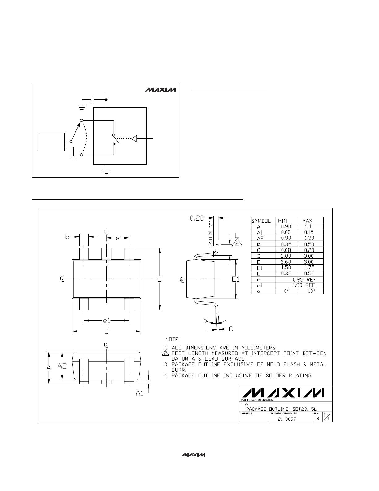
Package Information
V+
10nF
V+
COM
CAPACITANCE
METER
f = 1MHz
NC or
NO
GND
IN
MAX4626
MAX4627
MAX4628
OR
V
INL
V
INH
SOT5L.EPS
 Loading...