

________________General Description
The MAX4617/MAX4618/MAX4619 are high-speed, lowvoltage, CMOS analog ICs configured as an 8-channel
multiplexer (MAX4617), two 4-channel multiplexers
(MAX4618), and three single-pole/double-throw (SPDT)
switches (MAX4619).
These CMOS devices can operate continuously with a
+2V to +5.5V single supply. Each switch can handle
Rail-to-Rail®analog signals. The off-leakage current is
only 1nA at TA= +25°C and 10nA at TA= +85°C.
All digital inputs have 0.8V to 2.4V logic thresholds,
ensuring TTL/CMOS-logic compatibility when using a
single +5V supply.
________________________Applications
Battery-Operated Equipment
Audio/Video Signal Routing
Low-Voltage Data-Acquisition Systems
Communications Circuits
____________________________Features
♦ Fast Switching Times
15ns t
ON
10ns t
OFF
♦ Pin Compatible with Industry-Standard
74HC4051/74HC4052/74HC4053 and
MAX4581/MAX4582/MAX4583
♦ Guaranteed On-Resistance
10Ω max (+5V Supply)
20Ω max (+3V Supply)
♦ Guaranteed 1Ω On-Resistance Match Between
Channels (single +5V supply)
♦ Guaranteed Low Off-Leakage Current:
1nA at +25°C
♦ Guaranteed Low On-Leakage Current:
1nA at +25°C
♦ +2V to +5.5V Single-Supply Operation
♦ TTL/CMOS-Logic Compatible
♦ Low Crosstalk: <-96dB
♦ High Off-Isolation: <-93dB
♦ Low Distortion: <0.017% (600Ω)
MAX4617/MAX4618/MAX4619
High-Speed, Low-Voltage, CMOS Analog
Multiplexers/Switches
________________________________________________________________
Maxim Integrated Products
1
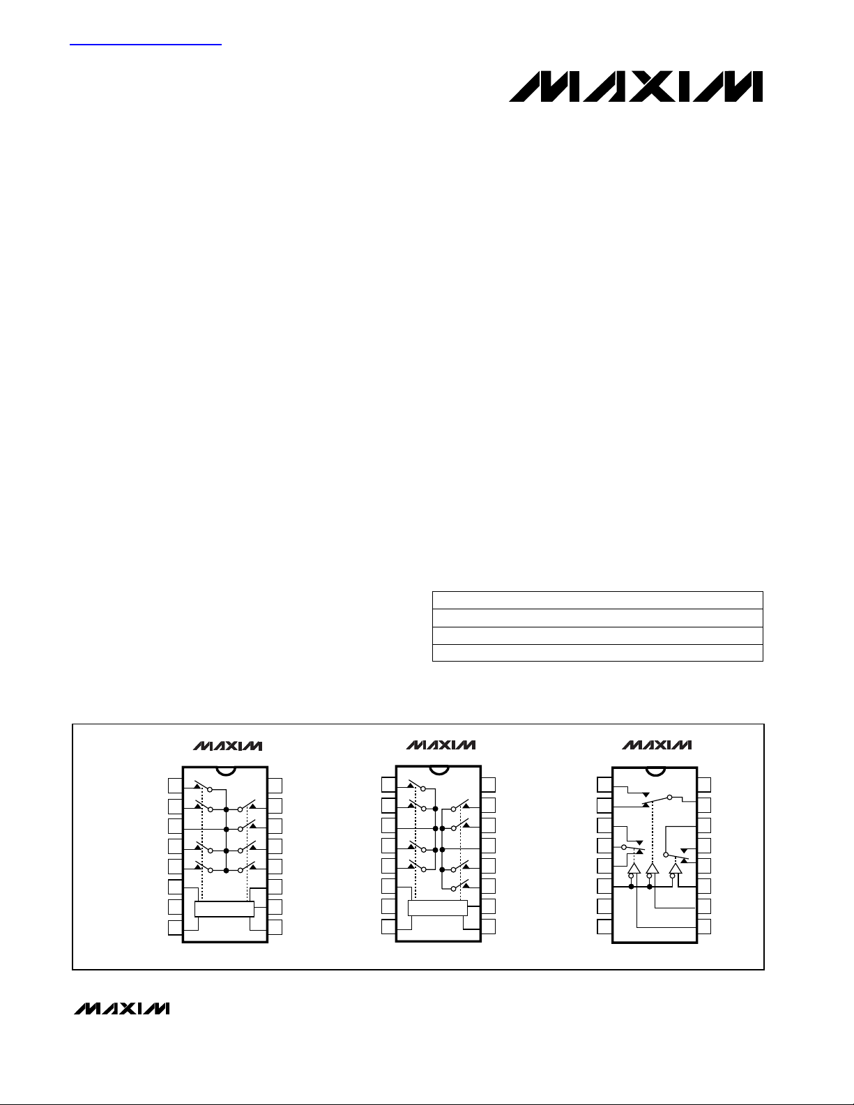
____________________________________Pin Configurations/Functional Diagrams
19-1502; Rev 0; 7/99
_______________Ordering Information
Ordering Information continued at end of data sheet.
Rail-to-Rail is a registered trademark of Nippon Motorola, Ltd.
For free samples & the latest literature: http://www.maxim-ic.com, or phone 1-800-998-8800.
For small orders, phone 1-800-835-8769.
16 Plastic DIP
16 Narrow SO
16 TSSOP
PIN-PACKAGETEMP. RANGE
0°C to +70°C
0°C to +70°C
0°C to +70°CMAX4617CPE
MAX4617CSE
MAX4617CUE
PART
查询MAX4617供应商
TOP VIEW
MAX4617
Y0
Y2
Y
Y3
Y1
ENABLE
N.C.
GND
ENABLE
N.C.
GND
X4
1
X6
2
X
3
X7
4
X5
5
6
7
LOGIC
8
V
16
CC
X2
15
X1
14
X0
13
X3
12
11
A
10
B
9
C
DIP/SO/TSSOP
MAX4618
1
2
3
4
5
6
7
LOGIC
8
DIP/SO/TSSOP
V
16
CC
X2
15
X1
14
X
13
X0
12
11
X3
10
A
9
B
Y1
Y0
Z1
Z
Z0
ENABLE
N.C.
GND
MAX4619
1
2
3
4
5
6
7
8
DIP/SO/TSSOP
V
16
CC
Y
15
X
14
X1
13
X0
12
11
A
10
B
9
C
MAX4617/MAX4618/MAX4619
High-Speed, Low-Voltage, CMOS Analog
Multiplexers/Switches
2 _______________________________________________________________________________________
ABSOLUTE MAXIMUM RATINGS
ELECTRICAL CHARACTERISTICS—Single +5V Supply
(VCC= +4.5V to +5.5V, V_H= 2.4V, V_L= 0.8V, TA= T
MIN
to T
MAX
, unless otherwise noted. Typical values are at TA= +25°C.) (Note 2)
Stresses beyond those listed under “Absolute Maximum Ratings” may cause permanent damage to the device. These are stress ratings only, and functional
operation of the device at these or any other conditions beyond those indicated in the operational sections of the specifications is not implied. Exposure to
absolute maximum rating conditions for extended periods may affect device reliability.
Voltages Referenced to GND
V
CC,
A, B, C, or Enable...........................................-0.3V to +6V
Voltage into Any Analog Terminal
(Note 1).........................................................-0.3V to (V
CC
+ 0.3V)
Continuous Current into Any Terminal..............................±75mA
Peak Current, X_, Y_, Z_
(pulsed at 1ms, 10% duty cycle) .................................±200mA
Continuous Power Dissipation (T
A
= +70°C)
TSSOP (derate 6.7mW/°C above +70°C)......................533mW
Narrow SO (derate 8.70mW/°C above +70°C)..............696mW
Plastic DIP (derate 10.53mW/°C above +70°C) ..............842mW
Operating Temperature Ranges
MAX461_C_ _ ......................................................0°C to +70°C
MAX461_E_ _ ....................................................-40°C to +85°C
Storage Temperature Range .............................-65°C to +150°C
Lead Temperature (soldering, 10sec) .............................+300°C
Note 1: Voltages exceeding V
CC
or GND on any analog signal terminal are clamped by internal diodes. Limit forward-diode current
to maximum current rating.
C, E -10 10
-1 0.002 1
X, Y, Z On-Leakage
Current (Note 5)
I
X(ON)
,
I
Y(ON)
,
I
Z(ON)
nA
TA=
+25°C
C, E -10 10
-1 0.002 1
X, Y, Z Off-Leakage
Current (Note 5)
I
X(OFF)
,
I
Y(OFF)
,
I
Z(OFF)
nA
TA=
+25°C
C, E -10 10
-1 0.002 1
X_, Y_, Z_
Off-Leakage Current
(Note 5)
I
X_(OFF)
,
I
Y_(OFF)
,
I
Z_(OFF)
nA
TA=
+25°C
Input Voltage Low 0.8C, E
VAL, VBL,
V
CL,
V
ENABLEL
V
Input Voltage High
VAH, VBH,
V
CH,
V
ENABLEH
V2.4C, E
PARAMETER SYMBOL UNITSMIN TYP MAXCONDITIONS
1
13
0V
CC
810
1.2
0.2 1
Switch On-Resistance
Flatness (Note 4)
R
FLAT(ON)
Ω
Switch On-Resistance
Match Between
Channels (Note 3)
∆R
ON
C, E
Ω
TA=
+25°C
Switch On-Resistance R
ON
C, E
Ω
Analog-Signal Range VX, VY, V
Z
C, E V
TA=
+25°C
C, E
ANALOG SWITCH
VCC= 5.5V; VX, VY, VZ= 1V, 4.5V;
VX_, VY_, VZ_= 1V, 4.5V or floating
VCC= 5.5V; VEE= -5.5V;
VX_, VY_, VZ_= 4.5V, 1V;
VX, VY, VZ= 1V, 4.5V
VCC= 5.5V; VX_, VY_, VZ_= 4.5V, 1V;
V
X
, VY, VZ= 1V, 4.5V
VCC= 4.5V; IX, IY, IZ= 10mA;
VX, VY, VZ= 1V, 2V, 3V
VCC= 4.5V; IX, IY, IZ= 10mA;
VX, VY, VZ= 3V
VCC= 4.5V; IX, IY, IZ = 10mA;
VX, VY, VZ= 3V
DIGITAL I/O
MAX4617/MAX4618/MAX4619
High-Speed, Low-Voltage, CMOS Analog
Multiplexers/Switches
_______________________________________________________________________________________ 3
ELECTRICAL CHARACTERISTICS—Single +5V Supply (continued)
(VCC= +4.5V to +5.5V, V_H= 2.4V, V_L= 0.8V, TA= T
MIN
to T
MAX
, unless otherwise noted. Typical values are at TA= +25°C.) (Note 2)
C, E 18
TA= +25°C
Address Transition Time
(Note 6)
t
TRANS
ns
VX_, VY_, VZ_= 3V; RL= 300Ω; CL= 35pF;
Figure 2
715
C, E 13
TA= +25°C
Enable Turn-Off Time
(Note 6)
t
OFF
ns
VX_, VY_, VZ_= 3V; RL= 300Ω; CL= 35pF;
Figure 3
45 10
C, E -10 10
C, E
TA= +25°C
18
TA= +25°C
Enable Turn-On Time
(Note 6)
t
ON
ns
VX_, VY_, VZ_= 3V; RL= 300Ω; CL= 35pF;
Figure 3
715
Power-Supply Current I
CC
µAVCC= 5.5V; VA, VB, VC, V
ENABLE
= V
CC
or 0
-1 1
PARAMETER SYMBOL UNITSMIN TYP MAXCONDITIONS
TA= +25°C
Break-Before-Make Time
(Note 6)
t
BBM
ns
VX_, VY_, VZ_= 3V; RL= 300Ω; CL= 35pF;
Figure 4
0.2 1.5
Charge Injection
Q pC
TA= +25°C
C = 1nF, RS = 0, VS= 0, Figure 5 3
pF
Output Off-Capacitance
C
X(OFF)
,
C
Y(OFF)
,
C
Z(OFF)
TA= +25°C
VX_, VY_, V
Z_
= 0; f = 1MHz;
Figure 7
27
pF
Output On-Capacitance
C
X(ON)
,
C
Y(ON)
,
C
Z(ON)
TA= +25°C
VX_, VY_, V
Z_
= 0; f = 1MHz;
Figure 7
32
MAX4617
MAX4617
dB
Off-Isolation
V
ISO
TA= +25°C
-93
15
MAX4618
8.5MAX4619
21
15.5MAX4619
MAX4618
RL= 50Ω, f = 100kHz, Figure 6
%
Total Harmonic
Distortion
THD
TA= +25°C
RL= 600Ω, 1Vp-p, f = 20Hz to 20kHz 0.017
VPower-Supply Range V
CC
C, E
+2 +5.5
C, EInput Current High
IAH, IBH,
I
CH,
I
ENABLE
µAVA, VB, VC= V
ENABLE
= V
CC
-1 0.0003 1
C, EInput Current Low
IAL, IBL,
I
CL,
I
ENABLE
µAVA, VB, VC= V
ENABLE
= 0 -1 0.0003 1
Input Off-Capacitance
C
X_(OFF)
,
C
Y_(OFF)
,
C
Z_(OFF)
pF
TA= +25°C
VX_, VY_, V
Z_
= 0; f = 1MHz; Figure 7 5
dB
Channel-to-Channel
Crosstalk
V
CT
TA= +25°C
-96RL= 50Ω, f = 100kHz, Figure 6
POWER SUPPLY
SWITCH DYNAMIC CHARACTERISTICS
MAX4617/MAX4618/MAX4619
High-Speed, Low-Voltage, CMOS Analog
Multiplexers/Switches
4 _______________________________________________________________________________________
ELECTRICAL CHARACTERISTICS—Single +3.3V Supply
(VCC= +3V to +3.6V, V_H= 2.0V, V_L= 0.5V, TA= T
MIN
to T
MAX
, unless otherwise noted. Typical values are at TA= +25°C.) (Note 2)
C, E 0V
CC
V
VX_, VY_, VZ_,
VX, VY, V
Z
Analog-Signal Range
CONDITIONS MIN TYP MAX UNITS
C, E 25
820
VCC= 3V; IX, IY, IZ= 10mA;
VX, VY, VZ= 1.5V
Ω
SYMBOL
TA= +25°C
R
ON
PARAMETER
Switch On-Resistance
-1 0.0003 1VA, VB, VC= V
ENABLE
= 0 µA
IAL, IBL, ICL,
I
ENABLEL
Input Current Low C, E
920
VX_, VY_, VZ_= 1.5V; RL= 300Ω;
C
L
= 35pF; Figure 3
nst
ON
Enable Turn-On Time
(Note 6)
TA= +25°C
0.5 V
VAL, VBL, VCL,
V
ENABLEL
Input Voltage Low C, E
-1 0.0003 1VA, VB, VC= V
ENABLE
= V
CC
µA
IAH, IBH, ICH,
I
ENABLEH
Input Current High C, E
2.0 V
VAH, VBH, VCH,
V
ENABLEH
Input Voltage High C, E
25C, E
0.2 1.5
VX_, VY_, VZ_= 1.5V; RL= 300Ω; CL= 35pF
nst
BBM
Break-Before-Make Time
(Note 6)
TA= +25°C
615
VX_, VY_, VZ_= 1.5V; RL= 300Ω;
C
L
= 35pF; Figure 3
nst
OFF
Enable Turn-Off Time
(Note 6)
TA= +25°C
20C, E
920
VX_, VY_, VZ_= 1.5V/0; RL= 300Ω;
C
L
= 35pF; Figure 2
nst
TRANS
Address Transition
Time (Note 6)
TA= +25°C
25C, E
3C = 1nF, RS= 0, VS= 0, Figure 5 pCQ
Charge Injection
(Note 6)
TA= +25°C
C, E -10 10
-1 0.002 1
V
CC
= 3.6V; VX_, VY_, VZ_= 1V, 3V;
VX, VY, VZ= 3V, 1V
nA
TA= +25°C
I
X_(OFF)
,
I
Y_(OFF)
,
I
Z_(OFF)
X_, Y_, Z_ Off-Leakage
Current (Note 5)
C, E -10 10
-1 0.002 1
VCC= 3.6V; VX_, VY_, VZ_= 1V, 3V;
VX, VY, VZ= 3V, 1V
nA
TA= +25°C
I
X(OFF)
,
I
Y(OFF)
,
I
Z(OFF)
X, Y, Z Off-Leakage
Current (Note 6)
C, E -10 10
-1 0.002 1
VCC= 3.6V; VX, VY, VZ= 3V, 1V;
VX_, VY_, VZ_= 3V, 1V, or floating
nA
TA= +25°C
I
X(ON)
,
I
Y(ON)
,
I
Z(ON)
X, Y, Z On-Leakage
Current (Note 6)
1
VCC= 3.6V,
VA, VB, VC, V
ENABLE
= VCCor 0
µAI
CC
Power-Supply Current
TA= +25°C
10C, E
ANALOG SWITCH
POWER SUPPLY
SWITCH DYNAMIC CHARACTERISTICS
DIGITAL I/O
MAX4617/MAX4618/MAX4619
High-Speed, Low-Voltage, CMOS Analog
Multiplexers/Switches
_______________________________________________________________________________________ 5
Note 2: The algebraic convention is used in this data sheet; the most negative value is shown in the minimum column.
Note 3: ∆R
ON
= R
ON(MAX)
- R
ON(MIN)
.
Note 4: Flatness is defined as the difference between the maximum and minimum value of on-resistance as measured over the specified
analog signal ranges; i.e., V
X_
, VY_, VZ_= 3V to 0 and 0 to -3V.
Note 5: Leakage parameters are 100% tested at maximum-rated hot operating temperature, and guaranteed by correlation at TA= +25°C.
Note 6: Guaranteed by design, not production tested.
ELECTRICAL CHARACTERISTICS—Single +2.5V Supply
(VCC= +2.5V, TA= T
MIN
to T
MAX
, unless otherwise noted. Typical values are at TA= +25°C.) (Note 2)
CONDITIONS MIN TYP MAX UNITSSYMBOLPARAMETER
C, E 100
30 60
VCC= 2.5V; IX, IY, IZ= 10mA;
VX, VY, VZ= 1.2V
Ω
TA= +25°C
R
ON
Switch On-Resistance
12
VX_, VY_, VZ_= 1V; RL= 300Ω;
C
L
= 35pF; Figure 3
ns
TA= +25°C
t
ON
Enable Turn-On Time
(Note 6)
10
VX_, VY_, VZ_= 1V; RL= 300Ω;
C
L
= 35pF; Figure 3
ns
TA= +25°C
t
OFF
Enable Turn-Off Time
(Note 6)
12
VX_, VY_, VZ_= 1V; RL= 300Ω;
C
L
= 35pF; Figure 3
ns
TA= +25°C
t
TRANS
Address Transition
Time (Note 6)
SWITCH DYNAMIC CHARACTERISTICS
ANALOG SWITCH

MAX4617/MAX4618/MAX4619
High-Speed, Low-Voltage, CMOS Analog
Multiplexers/Switches
6 _______________________________________________________________________________________
Typical Operating Characteristics
(VCC= +5V, GND = 0, TA= +25°C, unless otherwise noted.)
ON-RESISTANCE vs.
V
, VY, VZ AND TEMPERATURE
ON-RESISTANCE vs. VX, VY, V
25
20
15
10
ON-RESISTANCE (Ω)
5
0
0 2.5 3.0 3.5 4.0 4.50.5 1.0 1.5 2.0 5.0
VCC = +2V
VCC = +2.5V
VCC = +3V
VX, VY, VZ (V)
Z
VCC = +5V
MAX4617 toc01
5.0
4.5
4.0
3.5
3.0
(Ω)
2.5
ON
R
2.0
1.5
1.0
0.5
X
TA = +85°C
TA = +70°C
TA = +25°C
TA = 0°C
TA = -40°C
0
0 2.01.50.5 1.0 2.5 3.0 3.5 4.0 4.5 5.0
VX, VY, VZ (V)
MAX4617 toc02
OFF-LEAKAGE vs. TEMPERATURE
1000
100
10
1
OFF-LEAKAGE (pA)
0.1
0.01
-40 100020406080-20
TEMPERATURE (°C)
IX, IY, I
IX_, IY_, IZ_
MAX4617 toc03
Z
ON-LEAKAGE vs. TEMPERATURE
100
MAX4617 toc04
10
ON-LEAKAGE (pA)
1
0.1
-40 0-20 20 40 60 80 100
TEMPERATURE (°C)
SUPPLY CURRENT vs. TEMPERATURE
10,000
1000
(pA)
CC
I
VA, VB, VC, V
100
10
ENABLE
= 0, 5V
MAX4617 toc06
CHARGE INJECTION vs. VX, VY, V
20
18
16
14
12
10
8
6
CHARGE INJECTION (pC)
4
2
0
0 1.0 1.5 2.0 2.50.5 3.0 3.5 4.0 4.5 5.0
VX, VY, VZ (V)
SUPPLY CURRENT vs.
LOGIC VOLTAGE
2.5
(mA)
CC
I
2.0
1.5
1.0
0.5
VCC = +3V
VCC = +5V
VCC = +2V
Z
MAX4617 toc05
MAX4617 toc07
1
-40 20 6040-20 0 10080
TEMPERATURE (°C)
0
0 5.02.01.00.5 1.5 3.53.02.5 4.54.0
VA, VB, VC, V
ENABLE
(V)

MAX4617/MAX4618/MAX4619
High-Speed, Low-Voltage, CMOS Analog
Multiplexers/Switches
_______________________________________________________________________________________
7
Typical Operating Characteristics (continued)
(VCC= +5V, GND = 0, TA= +25°C, unless otherwise noted.)
INPUT HIGH LOGIC THRESHOLD
1.8
1.6
(V)
ENABLE
, V
1.4
C
, V
B
, V
A
V
1.2
1.0
2.0 2.5 3.0 4.03.5 4.5 5.0
0.025
0.02
0.015
0.01
0.005
vs. SUPPLY VOLTAGE
VCC (V)
TOTAL HARMONIC DISTORTION
vs. FREQUENCY
VCC = +3V,
1Vp-p SIGNAL
IN = OUT = 600Ω
VCC = +3.3V,
1Vp-p SIGNAL
VCC = 2.5V,
1Vp-p SIGNAL
VCC = +5V,
1Vp-p SIGNAL
MAX4617 toc08
MAX4617 toc10
0
-10
-20
-30
-40
-50
GAIN (dB)
-60
-70
-80
-90
-100
FREQUENCY RESPONSE
ON-LOSS
IN = OUT = 50Ω
ON-PHASE
OFF-ISOLATION
10k 100k 1M 10M 100M 500M
FREQUENCY (Hz)
SWITCHING TIME vs. VOLTAGE
14
12
10
8
6
SWITCHING TIMES (ns)
4
2
MAX4617 toc09
180
144
108
72
36
0
-36
-72
-108
-144
-180
MAX4617 toc11
PHASE (°)
0
0810462 1214161820
FREQUENCY (kHz)
0
2.0 3.0 3.52.5 4.0 4.5 5.0 5.5
V+ (V)

MAX4617/MAX4618/MAX4619
High-Speed, Low-Voltage, CMOS Analog
Multiplexers/Switches
8 _______________________________________________________________________________________
__________Applications Information
Power-Supply Considerations
Overview
The MAX4617/MAX4618/MAX4619 construction is typical of most CMOS analog switches. They have two supply pins: VCCand GND. VCCand GND are used to drive
the internal CMOS switches and set the limits of the analog voltage on any switch. Reverse ESD-protection
diodes are internally connected between each analogsignal pin and both VCCand GND. If any analog signal
exceeds VCCor GND, one of these diodes conducts.
During normal operation, these and other reversebiased ESD diodes leak, forming the only current drawn
from VCCor GND.
Virtually all the analog leakage current comes from the
ESD diodes. Although the ESD diodes on a given signal
pin are identical and therefore fairly well balanced, they
are reverse biased differently. Each is biased by either
V
CC
or GND and the analog signal. This means their
leakages will vary as the signal varies. The
difference
in
the two diode leakages to the VCCand GND pins constitutes the analog-signal-path leakage current. All analog leakage current flows between each pin and one of
the supply terminals, not to the other switch terminal.
This is why both sides of a given switch can show leakage currents of either the same or opposite polarity.
VCCand GND power the internal logic and set the input
logic limits. Logic inputs have ESD-protection diodes to
ground.
Note: Input and output pins are identical and interchangeable. Any may be considered an input or output; signals pass equally well
in both directions.
Digital Enable Input. Normally connect to GND. Can be driven
to logic high to set all switches off.
66
No Connection. Not Internally connected.77
Ground88
Digital Address “A” Input1011
Digital Address “B” Input910
Analog Switch “X” Normally Open Input——
Analog Switch “X” Normally Closed Input——
Analog Switch “Y” Normally Open Input——
Analog Switch “Y” Normally Closed Input——
Analog Switch “X” Output13—
Analog Switch “X” Inputs 0–312, 14, 15, 11—
Analog Switch Output—3
Analog Switch Inputs 0–7—
13, 14, 15,
12, 1, 5, 2, 4
FUNCTION
Analog Switch “Z” Normally Closed Input——
Analog Switch “Z” Normally Open Input——
Analog Switch “Z” Output——
Digital Address “C” Input—9
Analog Switch “Y” Inputs 0–31, 5, 2, 4—
Analog Switch “Y” Output3—
ENABLE6
N.C.7
GND8
A11
B10
X113
X012
Y11
Y02
X14
X0, X1, X2, X3—
X—
X0–X7—
NAME
Z05
Z13
Z4
C9
Y0, Y1, Y2, Y3—
Y15
MAX4617
MAX4618 MAX4619
Positive Analog and Digital Supply Voltage Input1616 V
CC
16
PIN
Pin Description

MAX4617/MAX4618/MAX4619
High-Speed, Low-Voltage, CMOS Analog
Multiplexers/Switches
_______________________________________________________________________________________ 9
The logic-level thresholds are TTL/CMOS compatible
when VCCis +5V. As VCCrises, the threshold increases; as VCCfalls, the threshold decreases. For example,
when VCC= +3V the guaranteed minimum logic-high
threshold decreases to 2.0V
Power Supply
These devices operate from a single supply between
+2.5V and +5.5V. All of the bipolar precautions must be
observed. At room temperature, they actually “work”
with a single supply near or below +2V, although as
supply voltage decreases, switch on-resistance
becomes very high.
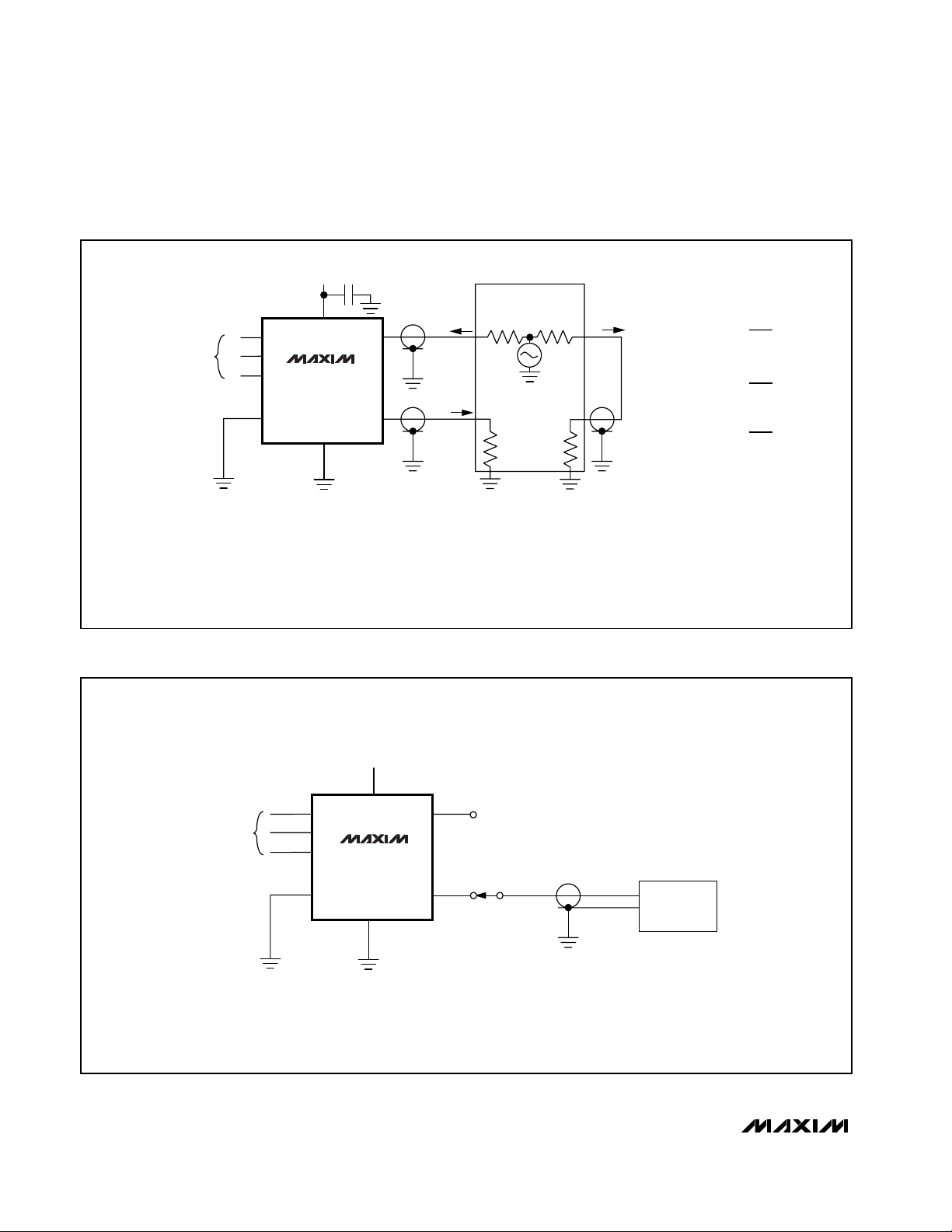
Overvoltage Protection
Proper power-supply sequencing is recommended for
all CMOS devices. Do not exceed the absolute maximum ratings because stresses beyond the listed ratings can cause permanent damage to the devices.
Always sequence VCCon first, followed by the logic
inputs and analog signals. If power-supply sequencing
is not possible, add two small signal diodes (D1, D2) in
series with the supply pins for overvoltage protection
(Figure 1).
Adding diodes reduces the analog-signal range to one
diode drop below VCCand one diode drop above
GND, but does not affect the devices’ low switch resistance and low leakage characteristics. Device operation is unchanged, and the difference between V
CC
and GND should not exceed 6V. These protection
diodes are not recommended if signal levels must
extend to ground.
High-Frequency Performance
In 50Ω systems, signal response is reasonably flat up
to 50MHz (see
Typical Operating Characteristics
).
Above 20MHz, the on-response has several minor
peaks that are highly layout dependent. The problem is
not turning the switch on, but turning it off. The off-state
switch acts like a capacitor and passes higher frequencies with less attenuation. At 10MHz, off-isolation is
about -50dB in 50Ω systems, becoming worse (approximately 20dB per decade) as frequency increases.
Higher circuit impedances also degrade off-isolation.
Adjacent channel attenuation is about 3dB above that
of a bare IC socket and is entirely due to capacitive
coupling.
Pin Nomenclature
The MAX4617/MAX4618/MAX4619 are pin compatible
with the industry-standard 74HC4051/74HC4052/
74HC4053 and the MAX4581/MAX4582/MAX4583. In
single-supply applications, they function identically and
have identical logic diagrams, although these parts differ electrically.
The pin designations and logic diagrams in this data
sheet conform to the original 1972 specifications published by RCA for the CD4051/CD4052/CD4053. These
designations differ from the standard Maxim switch and
mux designations found on other Maxim data sheets
(including the MAX4051/MAX4052/MAX4053) and may
cause confusion. Designers who feel more comfortable
with Maxim’s standard designations are advised that
the pin designations and logic diagrams on the
MAX4051/MAX4052/MAX4053 data sheet may be freely
applied to the MAX4617/MAX4618/MAX4619.
Figure 1. Overvoltage Protection Using External Blocking
Diodes
V
CC
D1
EXTERNAL
BLOCKING DIODE
MAX4617
V
CC
*
X, Y, Z X_, Y_, Z_
*
V
EE
GND
*
*
D2
EXTERNAL
BLOCKING DIODE
*INTERNAL PROTECTION DIODES
MAX4618
MAX4619

MAX4617/MAX4618/MAX4619
High-Speed, Low-Voltage, CMOS Analog
Multiplexers/Switches
10 ______________________________________________________________________________________
ENABLE
INPUT
C* MAX4619
MAX4618
MAX4617A
B
SELECT INPUTS ON SWITCHES
L H
L H
X–X0,
Y–Y1,
Z–Z1
X–X2,
Y–Y2
X–X6LH
X–X1,
Y–Y1,
Z–Z1
X–X3,
Y–Y3
X–X7HH
L H
L H
X–X0,
Y–Y0,
Z–Z1
X–X0,
Y–Y0
X–X4LL
X–X1,
Y–Y0,
Z–Z1
X–X1,
Y–Y1
X–X5HL
L L
L L
X–X0,
Y–Y1,
Z–Z0
X–X2,
Y–Y2
X–X2LH
X–X1,
Y–Y1,
Z–Z0
X–X3,
Y–Y3
X–X3HH
L L
X–X1,
Y–Y0,
Z–Z0
X–X1,
Y–Y1
X–X1HL
L L
X–X0,
Y–Y0,
Z–Z0
X–X0,
Y–Y0
X–X0LL
All switches openAll switches openAll switches openXXH X
X = Don’t care
*
C not present on MAX4618.
Note: Input and output pins are identical and interchangeable. Either may be considered an input or output; signals pass equally
well in either direction.
Table 1. Truth Table/Switch Programming

MAX4617/MAX4618/MAX4619
High-Speed, Low-Voltage, CMOS Analog
Multiplexers/Switches
______________________________________________________________________________________ 11
Figure 2. Address Transition Times
______________________________________________Test Circuits/Timing Diagrams
V
VA, VB, VC
50Ω
V
, V
A
B
50Ω
A
B
C
ENABLE
A
B
ENABLE
CC
V
CC
MAX4617
GND
V
CC
V
CC
MAX4618
GND
X1–X7
X
, Y
0
X1, X2, Y1,
Y2. X3, Y3
X, Y
VA, VB, V
X0
X
V
CC
V
OUT
35pF
300Ω
VA, V
V
0
300Ω
CC
V
OUT
35pF
V
CC
C
50%
0
V
X0
90%
0
V
OUT
V
X7
t
TRANS
V
CC
B
50%
90%
t
TRANS
0
V
,
X0
V
Y0
90%
0
V
OUT
,
V
X3
V
Y3
t
TRANS
90%
t
TRANS
V
V
, VB, V
A
C
A, B, C
V
50Ω
MAX4619
ENABLE
GND
TEST EACH SECTION INDIVIDUALLY.
CC
CC
X1, Y1, Z1
X2, Y2, Z2
X, Y, Z
300Ω
V
VA, VB, V
CC
C
50%
0
V
,
X0
,
V
Y0
V
OUT
Z0
0
,
V
X1
,
V
Y1
V
Z1
t
TRANS
90%
V
CC
V
OUT
35pF
V
90%
t
TRANS

MAX4617/MAX4618/MAX4619
High-Speed, Low-Voltage, CMOS Analog
Multiplexers/Switches
12 ______________________________________________________________________________________
Figure 3. Enable Switching Times
_________________________________Test Circuits/Timing Diagrams (continued)
V
V
ENABLE
V
ENABLE
50Ω
50Ω
A
B
C
ENABLE
A
B
ENABLE
CC
V
CC
MAX4617
GND
V
CC
V
CC
X1–X3, Y1–Y3
MAX4618
GND
X1–X7
X0, Y0
X, Y
X0
X
300Ω
300Ω
V
CC
V
OUT
35pF
V
CC
V
OUT
35pF
V
ENABLE
V
ENABLE
V
CC
0
V
X0
V
OUT
0
t
ON
V
CC
0
,
V
X0
V
Y0
V
OUT
0
t
ON
50%
90%
90%
50%
90%
90%
V
V
ENABLE
50Ω
A
B
C
ENABLE
CC
V
CC
MAX4619
GND
X1, Y1, Z1
X0, Y0, Z0
X, Y, Z
300Ω
V
CC
V
OUT
35pF
V
ENABLE
V
CC
0
VX0,
,
V
Y0
V
Z0
V
OUT
VX1,
,
V
Y1
V
Z1
t
ON
50%
90%
90%
t
OFF
t
OFF
t
OFF
TEST EACH SECTION INDIVIDUALLY.

MAX4617/MAX4618/MAX4619
High-Speed, Low-Voltage, CMOS Analog
Multiplexers/Switches
______________________________________________________________________________________ 13
Figure 4. Break-Before-Make Interval
Figure 5. Charge Injection
_________________________________Test Circuits/Timing Diagrams (continued)
MAX4618
GND
50%
V
CC
V
CC
X0–X3,
Y0–Y3
X, Y
80%
300Ω
t
R
t
F
< 20ns
< 20ns
V
CC
V
OUT
35pF
VA, VB, V
50Ω
VA, VB, V
50Ω
V
CC
C
A
B
C
V
CC
X0–X7
V
CC
VA, V
50Ω
B
A
B
MAX4617
V
35pF
35pF
OUT
VA, VB, V
V
OUT
V+
C
0
V
, VY, V
X
Z
V
OUT
ENABLE
GND
V
CC
C
A, B, C
V
CC
X0, X1, Y0,
Y1, Z0, Z1
X
300Ω
V
CC
MAX4619
ENABLE
X, Y, Z
GND
300Ω
ENABLE
TEST EACH SECTION INDIVIDUALLY.
V
CC
V
CHANNEL
SELECT
V
ENABLE
TEST EACH SECTION INDIVIDUALLY.
A
B
C
ENABLE
50Ω
CC
MAX4617
MAX4618
MAX4619
GND
X_, Y_, Z_
X, Y, Z
C
L
1000pF
0
t
BBM
V
V
ENABLE
V
OUT
CC
0
V
OUT
∆ V
IS THE MEASURED VOLTAGE DUE TO CHARGE-
OUT
TRANSFER ERROR Q WHEN THE CHANNEL TURNS OFF.
Q = ∆ V
· C
OUT
L
∆ V
OUT
MAX4617/MAX4618/MAX4619
High-Speed, Low-Voltage, CMOS Analog
Multiplexers/Switches
14 ______________________________________________________________________________________
Figure 6. Off-Isolation, On-Loss, and Crosstalk
Figure 7. Capacitance
_________________________________Test Circuits/Timing Diagrams (continued)
V
10nF
CC
NETWORK
V
IN
CHANNEL
SELECT
V
CC
A
B
C
X_, Y_, Z_
MAX4617
MAX4618
V
MAX4619
ENABLE
NOTES: MEASUREMENTS ARE STANDARDIZED AGAINST SHORT AT SOCKET TERMINALS.
OFF ISOLATION IS MEASURED BETWEEN COM AND "OFF" NO TERMINAL ON EACH SWITCH.
ON LOSS IS MEASURED BETWEEN COM AND "ON" NO TERMINAL ON EACH SWITCH.
CROSSTALK (MAX4618/MAX4619) IS MEASURED FROM ONE CHANNEL (A, B, C) TO ALL OTHER CHANNELS.
SIGNAL DIRECTION THROUGH SWITCH IS REVERSED; WORST VALUES ARE RECORDED.
X, Y, Z
GND
OUT
50Ω
MEAS.
50Ω 50Ω
ANALYZER
50Ω
REF.
OFF-ISOLATION = 20log
ON-LOSS = 20log
CROSSTALK = 20log
V
OUT
V
IN
V
OUT
V
IN
V
OUT
V
IN
V
CC
V
CC
X_, Y_, Z_
MAX4617
MAX4618
MAX4619
GND
X, Y, Z
CHANNEL
SELECT
A
B
C
ENABLE
1MHz
CAPACITANCE
ANALYZER
MAX4617/MAX4618/MAX4619
High-Speed, Low-Voltage, CMOS Analog
Multiplexers/Switches
______________________________________________________________________________________ 15
___________________Chip Information_Ordering Information (continued)
TRANSISTOR COUNT: 244
PART
MAX4617EUE -40°C to +85°C
TEMP. RANGE PIN-PACKAGE
16 TSSOP
MAX4617ESE
MAX4617EPE -40°C to +85°C
-40°C to +85°C 16 Narrow SO
16 Plastic DIP
MAX4618CUE
MAX4618CSE
MAX4618CPE 0°C to +70°C
0°C to +70°C
0°C to +70°C 16 TSSOP
16 Narrow SO
16 Plastic DIP
MAX4618EUE -40°C to +85°C 16 TSSOP
MAX4618ESE -40°C to +85°C 16 Narrow SO
MAX4618EPE -40°C to +85°C 16 Plastic DIP
MAX4619EUE -40°C to +85°C 16 TSSOP
MAX4619CUE
MAX4619CSE 0°C to +70°C
0°C to +70°C 16 TSSOP
16 Narrow SO
MAX4619CPE 0°C to +70°C 16 Plastic DIP
MAX4619ESE -40°C to +85°C 16 Narrow SO
MAX4619EPE -40°C to +85°C 16 Plastic DIP

MAX4617/MAX4618/MAX4619
High-Speed, Low-Voltage, CMOS Analog
Multiplexers/Switches
Maxim cannot assume responsibility for use of any circuitry other than circuitry entirely embodied in a Maxim product. No circuit patent licenses are
implied. Maxim reserves the right to change the circuitry and specifications without notice at any time.
16
____________________Maxim Integrated Products, 120 San Gabriel Drive, Sunnyvale, CA 94086 408-737-7600
© 1999 Maxim Integrated Products Printed USA is a registered trademark of Maxim Integrated Products.
________________________________________________________Package Information
TSSOP.EPS
 Loading...