

Page 1
________________General Description
The MAX4613 quad analog switch features on-resistance matching (4Ω max) between switches and guarantees on-resistance flatness over the signal range (9Ω
max). This low on-resistance switch conducts equally
well in either direction. It guarantees low charge injection (10pC max), low power consumption (35µW max),
and an electrostatic discharge (ESD) tolerance of
2000V minimum per Method 3015.7. The new design
offers lower off-leakage current over temperature (less
than 5nA at +85°C).
The MAX4613 quad, single-pole/single-throw (SPST)
analog switch has two normally closed switches and
two normally open switches. Switching times are less
than 250ns for tONand less than 70ns for t
OFF
.
Operation is from a single +4.5V to +40V supply or
bipolar ±4.5V to ±20V supplies.
________________________Applications
Sample-and-Hold Circuits Communication Systems
Test Equipment Battery-Operated Systems
Heads-Up Displays PBX, PABX
Guidance and Control Systems Audio Signal Routing
Military Radios Modems/Faxes
____________________________Features
♦ Pin Compatible with Industry-Standard DG213
♦ Guaranteed RONMatch Between Channels
(4Ω max)
♦ Guaranteed R
FLAT(ON)
Over Signal Range
(9Ω max)
♦ Guaranteed Charge Injection (10pC max)
♦ Low Off-Leakage Current Over Temperature
(<5nA at +85°C)
♦ Withstands 2000V min ESD, per Method 3015.7
♦ Low R
DS(ON)
(85Ω max)
♦ Single-Supply Operation +4.5V to +40V
Bipolar-Supply Operation ±4.5V to ±20V
♦ Low Power Consumption (35µW max)
♦ Rail-to-Rail Signal Handling
♦ TTL/CMOS-Logic Compatible
MAX4613
Quad, SPST Analog Switch
________________________________________________________________ Maxim Integrated Products 1
19-1362; Rev 3; 6/07
________________Ordering Information
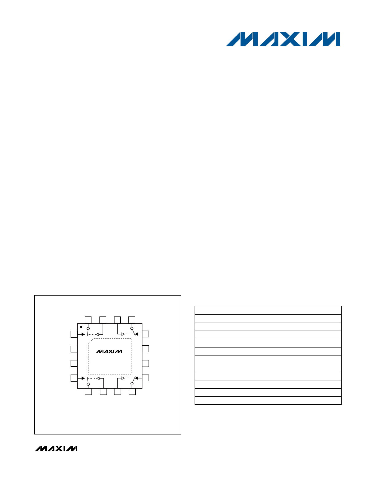
Pin Configurations/
___Functional Diagrams/TruthTable
*Contact factory for dice specifications.
**Contact factory for availability.
***EP = Exposed Pad
For pricing, delivery, and ordering information, please contact Maxim Direct at 1-888-629-4642,
or visit Maxim’s website at www.maxim-ic.com.
Pin Configurations continued at end of data sheet.
TOP VIEW
S1
V-
GND
S4
*EP = EXPOSED PAD, CONNECT EP TO V+
D1
IN1
IN2
D2
16
1
2
3
4
5
D4
14 13
15
MAX4613
6
7
IN4
THIN QFN
IN3
*EP
S2
12
11
V+
10
V
L
9
S3
8
D3
PART TEMP RANGE PIN-PACKAGE
MAX4613CPE 0°C to +70°C 16 Plastic DIP
MAX4613CSE 0°C to +70°C 16 Narrow SO
MAX4613CEE 0°C to +70°C 16 QSOP
MAX4613CUE 0°C to +70°C 16 TSSOP**
MAX4613CC/D 0°C to +70°C Dice*
MAX4613ETE -40°C to +85°C
MAX4613EPE -40°C to +85°C 16 P lastic DIP
MAX4613ESE -40°C to +85°C 16 Narrow SO
MAX4613EEE -40°C to +85°C 16 QSOP
MAX4613EUE -40°C to +85°C 16 TSSOP**
16 TQFN-EP***
(5mm x 5mm)
Page 2
MAX4613
Quad, SPST Analog Switch
2 _______________________________________________________________________________________
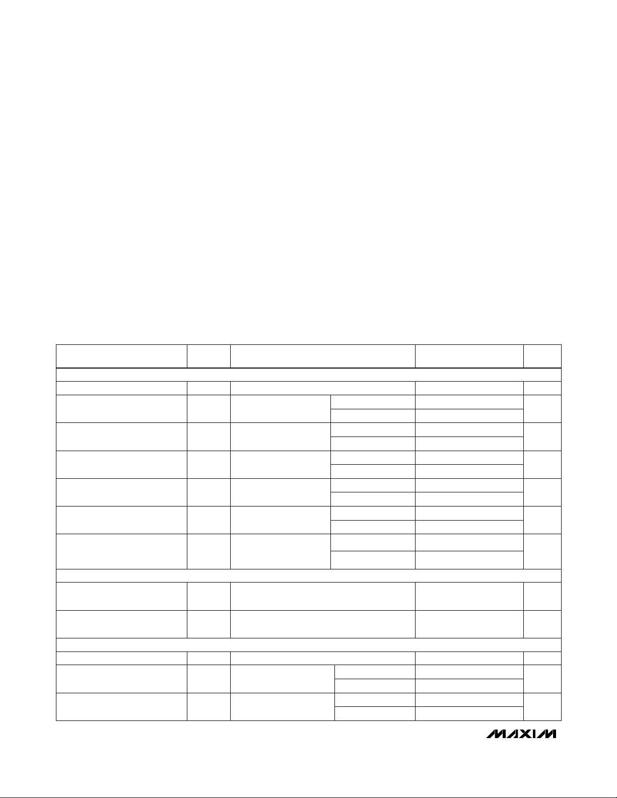
ABSOLUTE MAXIMUM RATINGS
ELECTRICAL CHARACTERISTICS—Dual Supplies
(V+ = 15V, V- = -15V, VL= 5V, GND = 0V, V
INH
= 2.4V, V
INL
= 0.8V, TA= T
MIN
to T
MAX
, unless otherwise noted.)
Stresses beyond those listed under “Absolute Maximum Ratings” may cause permanent damage to the device. These are stress ratings only, and functional
operation of the device at these or any other conditions beyond those indicated in the operational sections of the specifications is not implied. Exposure to
absolute maximum rating conditions for extended periods may affect device reliability.
Voltage Referenced to GND
V+ ......................................................................................+44V
V-.........................................................................................-44V
V+ to V- ..............................................................................+44V
V
L
...................................................(GND - 0.3V) to (V+ + 0.3V)
Digital Inputs V
S_VD_
(Note 1) ...................(V- - 2V) to (V+ + 2V)
or 30mA (whichever occurs first)
Continuous Current (any terminal) ......................................30mA
Peak Current, S_ or D_
(pulsed at 1ms, 10% duty cycle max) ...........................100mA
Continuous Power Dissipation (T
A
= +70°C)
Plastic DIP (derate 10.53mW/°C above +70°C)
.............842mW
Narrow SO (derate 8.70mW/°C above +70°C) .............696mW
QSOP (derate 8.3mW/°C above +70°C).......................667mW
Thin QFN (derate 33.3mW/°C above +70°C)..............2667mW
TSSOP (derate 6.7mW/°C above +70°C) .....................457mW
Operating Temperature Ranges
MAX4613C_ _ ......................................................0°C to +70°C
MAX4613E_ _ ...................................................-40°C to +85°C
Storage Temperature Range .............................-65°C to +165°C
Lead Temperature (soldering, 10sec) .............................+300°C
PARAMETER
TA= +25°C
SYMBOL
MIN TYP MAX
(Note 2)
TA= T
MIN
to T
MAX
-0.50 0.08 0.50
UNITS
TA= +25°C
R
FLAT(ON)
15
Drain-On Leakage Current
(Note 5)
I
D(ON)
or
I
S(ON)
ΩOn-Resistance Flatness (Note 4)
-10 10
TA= T
MIN
to T
MAX
9
On-Resistance Match
Between Channels (Note 4)
ΔR
DS(ON)
4
nA
TA= +25°C
TA= +25°C
85
Ω
TA= +25°C
TA= T
MIN
to T
MAX
-0.50 0.01 0.50
Source Leakage Current
(Note 5)
I
S(OFF)
-5 5
nA
Input Current with
Input Voltage High
VIN= 2.4V, all others = 0.8VI
INH
VIN= 0.8V, all others = 2.4V
-0.50 0.01 0.50
-0.5 -0.00001 0.5
Drain-Off Leakage Current
(Note 5)
µA
I
D(OFF)
-5 5
nA
Input Current with
Input Voltage Low
I
INL
-0.5 -0.00001 0.5 µA
Analog Signal Range V
ANALOG
-15 15 V
Drain-Source On-Resistance R
DS(ON)
55 70
TA= T
MIN
to T
MAX
CONDITIONS
VD= ±5V,
IS= 1mA
VD= ±14V,
V
S
= ±14V
5
VD= ±14V,
VS= 14V
VD= ±14V,
VS= 14V
(Note 3)
VD= ±10V,
I
S
= 1mA
TA= +25°C
TA= T
MIN
to T
MAX
Ω
TA= T
MIN
to T
MAX
VD= ±10V,
IS= 1mA
All channels on or off,
V
IN
= 0 or 5V
Positive Supply Current I+
-1 0.001 1
µA
Power-Supply Range V+, V- ±4.5 ±20.0 V
-5 5
TA= +25°C
TA= T
MIN
to T
MAX
All channels on or off,
VIN= 0 or 5V
Negative Supply Current I-
-1 0.001 1
µA
TA= T
MIN
to T
MAX
TA= +25°C
-5 5
SWITCH
INPUT
SUPPLY
Note 1: Signals on S_, D_, or IN_ exceeding V+ or V- are clamped by internal diodes. Limit forward current to maximum current rating.
±
±
Page 3
MAX4613
Quad, SPST Analog Switch
_______________________________________________________________________________________ 3
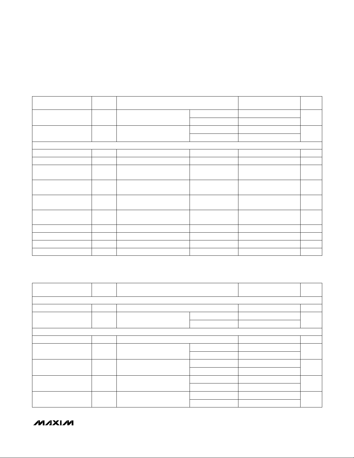
ELECTRICAL CHARACTERISTICS—Dual Supplies (continued)
(V+ = 15V, V- = -15V, VL= 5V, GND = 0V, V
INH
= 2.4V, V
INL
= 0.8V, TA= T
MIN
to T
MAX
, unless otherwise noted.)
PARAMETER
TA= +25°C
SYMBOL
MIN TYP MAX
(Note 2)
TA= T
MIN
to T
MAX
UNITS
TA= +25°C
TA= +25°C
TA= T
MIN
to T
MAX
TA= +25°C
TA= +25°CTurn-Off Time (Note 3) VS= ±10V, Figure 2
Source-On Capacitance
-1 0.001 1
90 120
Logic Supply Current I
L
-5 5
µA
Turn-On Time (Note 3) VS= ±10V, Figure 2t
ON
f = 1MHz, Figure 8
-1 -0.0001 1
150 250
ns
Ground Current
ns
I
GND
-5 5
µA
t
OFF
TA= +25°C
Off-Isolation Rejection
Ratio (Note 6)
RL= 50Ω, CL= 5pF,
f = 1MHz, Figure 5
OIRR 60 dB
TA= +25°C
Break-Before-Make Time
Delay (Note 3)
Figure 3t
D
520 ns
TA= +25°CCrosstalk (Note 7)
RL= 50Ω, CL= 5pF,
f = 1MHz, Figure 6
100 dB
TA= +25°CSource-Off Capacitance f = 1MHz, Figure 7C
S(OFF)
4 pF
TA= +25°CDrain-Off Capacitance f = 1MHz, Figure 7C
D(OFF)
4 pF
CONDITIONS
C
S(ON)
16 pF
TA= +25°C
All channels on or off,
VIN= 0 or 5V
Drain-On Capacitance f = 1MHz, Figure 8
All channels on or off,
V
IN
= 0 or 5V
C
D(ON)
16 pF
TA= +25°CCharge Injection (Note 3)
CL= 1nF, V
GEN
= 0,
R
GEN
= 0, Figure 4
Q 510pC
PARAMETER SYMBOL
MIN TYP MAX
(Note 2)
UNITS
Analog Signal Range V
ANALOG
012V
TA= +25°C 100 160
TA= T
MIN
to T
MAX
Drain-Source
On-Resistance
VL= 5V; VD= 3V, 8V;
IS= 1mA
R
DS(ON)
200
CONDITIONS
Ω
TA= +25°C -1 0.001 1
TA= T
MIN
to T
MAX
Power-Supply Current
All channels on or off,
V
IN
= 0 or 5V
I+
-5 5
µA
Power-Supply Range V+, V- 4.5 40 V
TA= +25°C -1 -0.0001 1
TA= T
MIN
to T
MAX
Negative Supply Current
All channels on or off,
VIN= 0 or 5V
I-
-5 5
µA
TA= +25°C -1 0.001 1
TA= T
MIN
to T
MAX
Logic Supply Current
All channels on or off,
V
IN
= 0 or 5V
I
L
-5 5
µA
TA= +25°C -1 -0.0001 1
TA= T
MIN
to T
MAX
Ground Current
All channels on or off,
V
IN
= 0 or 5V
I
GND
-5 5
µA
ELECTRICAL CHARACTERISTICS—Single Supply
(V+ = 12V, V- = 0V, VL= 5V, GND = 0V, V
INH
= 2.4V, V
INL
= 0.8V, TA= T
MIN
to T
MAX
, unless otherwise noted.)
DYNAMIC
SUPPLY
SWITCH
Page 4

MAX4613
Quad, SPST Analog Switch
4 _______________________________________________________________________________________
ELECTRICAL CHARACTERISTICS—Single Supply (continued)
(V+ = 12V, V- = 0, VL= 5V, GND = 0V, V
INH
= 2.4V, V
INL
= 0.8V, TA= T
MIN
to T
MAX
, unless otherwise noted.)
Note 2: Typical values are for design aid only, are not guaranteed and are not subject to production testing. The algebraic convention,
where the most negative value is a minimum and the most positive value a maximum, is used in this data sheet.
Note 3: Guaranteed by design.
Note 4: On-resistance match between channels and flatness are guaranteed only with bipolar-supply operation. Flatness is defined
as the difference between the maximum and the minimum value of on-resistance as measured at the extremes of the specified analog signal range.
Note 5:
Leakage parameters I
S(OFF)
, I
D(OFF)
, I
D(ON)
, and I
S(ON)
are 100% tested at the maximum rated hot temperature and guaranteed at +25°C.
Note 6: Off-Isolation Rejection Ratio = 20log (VD/VS).
Note 7: Between any two switches.
__________________________________________Typical Operating Characteristics
(TA = +25°C, unless otherwise noted.)
ON LEAKAGE
(nA)
-2
-1
0
1
2
-15 0 15
V
S
, V
D
(V)
TA = +125°C
TA = +85°C
V+ = 15V
V- = -15V
MAX4613-01
-10
-5
510
ON LEAKAGE CURRENTS
OFF LEAKAGE (nA)
-1
0
-0.5
0.5
1
V
S
, VD (V)
MAX4613-02
-15 0 15
-10
-5
510
TA = +125°C
V+ = 15V
V- = -15V
TA = +85°C
OFF LEAKAGE CURRENTS
V
IN
(V)
0
0.5
1.5
2.0
2.5
3.0
3.5
±5 ±10 ±15 ±20
BIPOLAR SUPPLY VOLTAGE (V)
MAX4613-03
IN LOW MAX
SWITCHING THRESHOLD vs.
BIPOLAR SUPPLY VOLTAGE
IN HIGH MIN
0
25
50
75
100
125
0 5 10 15 20
V
D
(V)
R
DS(ON)
(Ω)
MAX4613-04
V+ = 10V
V+ = 15V
V+ = 20V
150
V+ = 5V
ON-RESISTANCE vs. V
D
(UNIPOLAR SUPPLY VOLTAGE)
R
DS(ON)
(Ω)
30
60
90
120
-20 -10 0 10 20
V
D
(V)
0
MAX4613-05
ON-RESISTANCE vs. V
D
(BIPOLAR SUPPLY VOLTAGE)
V± = ±5V
V± = ±10V
V± = ±15V
V± = ±20V
R
DS(ON)
(Ω)
0
20
40
60
80
100
V
D
(V)
MAX4613-06
TA = +125°C
TA = -55°C
TA = +25°C
V+ = 15V, V- = -15V
-15 0 15
-10
-5
510
ON-RESISTANCE vs. VD (BIPOLAR
SUPPLY VOLTAGE AND TEMPERATURE)
PARAMETER SYMBOL
MIN TYP MAX
(Note 2)
UNITS
TA= +25°C 300 400VS = 8V, Figure 2
TA= +25°C
nst
ON
Turn-On Time (Note 3)
TA= +25°C 60 200VS = 8V, Figure 2
510
nst
OFF
Turn-Off Time (Note 3)
CL= 1nF, V
GEN
= 0,
R
GEN
= 0, Figure 4
pCQCharge Injection (Note 3)
CONDITIONS
DYNAMIC
Page 5

MAX4613
Quad, SPST Analog Switch
_______________________________________________________________________________________ 5
_____________________________Typical Operating Characteristics (continued)
(TA = +25°C, unless otherwise noted.)
0
25
50
75
100
125
150
R
DS(ON)
(Ω)
04 812
V
D
(V)
MAX4613-07
TA = +125°C
TA = +25°C
TA = -40°C
V+ = 12V
V- = 0
ON-RESISTANCE vs. V
D
(UNIPOLAR
SUPPLY VOLTAGE AND TEMPERATURE)
TIME (ns)
0
40
80
120
160
±5 ±10 ±15 ±20
BIPOLAR SUPPLY VOLTAGE (V)
MAX4613-08
t
ON
t
OFF
SWITCHING TIME vs.
BIPOLAR SUPPLY VOLTAGE
TIME (ns)
0
50
100
150
200
10 15 20 25
UNIPOLAR SUPPLY VOLTAGE (V)
V- = 0
MAX4613-09
t
ON
t
OFF
SWITCHING TIME vs.
UNIPOLAR SUPPLY VOLTAGE
Q (pC)
-20
0
-10
20
10
-15 -10 0 10 15
V
D
(V)
MAX4613-10
CHARGE INJECTION vs.
V
D
VOLTAGE
V+ = 15V
V- = -15V
C
L
= 1nF
Q (pC)
-10
0
5
-5
051015
VD (V)
MAX4613-11
10
CHARGE INJECTION vs.
V
D
VOLTAGE
V+ = 12V
V- = 0V
C
L
= 1nF
Page 6

MAX4613
Applications Information
General Operation
1) Switches are open when power is off.
2) IN_, D_, and S_ should not exceed V+ or V-, even
with the power off.
3) Switch leakage is from each analog switch terminal
to V+ or V-, not to other switch terminals.
Operation with Supply Voltages
Other than ±15V
Using supply voltages less than ±15V will reduce the
analog signal range. The MAX4613 operates with
±4.5V to ±20V bipolar supplies or with a +4.5V to +40V
single supply; connect V- to GND when operating with
a single supply. Also, all device types can operate with
unbalanced supplies such as +24V and -5V. VLmust
be connected to +5V to be TTL compatible, or to V+ for
CMOS-logic level inputs. The Typical Operating
Characteristics graphs show typical on-resistance with
±20V, ±15V, ±10V, and ±5V supplies. (Switching times
increase by a factor of two or more for operation at ±5V.)
Overvoltage Protection
Proper power-supply sequencing is recommended
for all CMOS devices. Do not exceed the absolute
maximum ratings because stresses beyond the listed ratings may cause permanent damage to the
devices. Always sequence V+ on first, followed by
VL, V-, and logic inputs. If power-supply sequencing
is not possible, add two small, external signal
diodes in series with supply pins for overvoltage
protection (Figure 1). Adding diodes reduces the
analog signal range to 1V below V+ and 1V above
V-, but low switch resistance and low leakage characteristics are unaffected. Device operation is
unchanged, and the difference between V+ and Vshould not exceed +44V.
Quad, SPST Analog Switch
6 _______________________________________________________________________________________
Pin Description
Figure 1. Overvoltage Protection Using External Blocking Diodes
PIN
DIP/SO/TSSOP THIN QFN
1, 8, 9, 16 6, 7, 14, 15 IN1–IN4 Logic Control Input
2, 7, 10, 15 5, 8, 13, 16 D1–D4 Analog-Switch Drain Output
3, 6, 11, 14 1, 4, 9, 12 S1–S4 Analog-Switch Source Output
4 2 V- Negative-Supply Voltage Input
5 3 GND Ground
12 10 V
13 11 V+ Positive-Supply Voltage Input—Connected to Substrate
— EP PAD Exposed Pad. Connect PAD to V+.
NAME FUNCTION
L
Logic-Supply Voltage Input
V+
S
V
g
D
V-
Page 7

MAX4613
Quad, SPST Analog Switch
_______________________________________________________________________________________ 7
Figure 2. Switching Time
Figure 3. Break-Before-Make Test Circuit
Timing Diagrams/Test Circuits
____________________Revision History
Pages changed at Rev 3: 1, 9, 10
LOGIC
+3V
INPUT
0V
SWITCH
OUTPUT
LOGIC INPUT WAVEFORM IS INVERTED FOR SWITCHES
THAT HAVE THE OPPOSITE LOGIC SENSE.
SWITCH
LOGIC
INPUT
REPEAT TEST FOR CHANNELS 2, 3, AND 4.
C
0V
INPUT
+3V
INCLUDES FIXTURE AND STRAY CAPACITANCE.
L
D_
IN_
V
t
+5V
V
GND
50%
t
OFF
OUT
0.8 x V
OUT
ON
+15V
L
V+
S_
V-
-15V
tf < 20ns
tr < 20ns
0.8 x V
MAX4613
R
L
V
= V
OUT
OUT
C
D
( )
RL + R
L
R
DS(ON)
LOGIC
INPUT
SWITCH
OUTPUT
SWITCH
OUTPUT
V
V
OUT
L
V
LOGIC
INPUT
D
+3V
0V
V
D
0V
V
D
0V
+5V
D
= 10V
= 10V
D_
D_
IN_
GND
C
INCLUDES FIXTURE AND STRAY CAPACITANCE. LOGIC 0 INPUT.
L
50%
V
O1
0.9V
O
V
O2
t
D
+15V
V
L
0V
V+
S_
S_
V-
-15V
MAX4613
R
L2
t
D
V
O2
RL = 1000Ω
C
= 35pF
L
0.9V
O
V
O1
R
L1
C
L2
C
L1
Page 8

MAX4613
Quad, SPST Analog Switch
8 _______________________________________________________________________________________
Figure 4. Charge Injection
_________________________________Timing Diagrams/Test Circuits (continued)
Figure 5. Off-Isolation Rejection Ratio
Figure 6. Crosstalk
Figure 7. Source/Drain-Off Capacitance
Figure 8. Source/Drain-On Capacitance
V
OUT
V
IN
R
GEN
V
GEN
Q = ΔV
S_
+5V
+15V
ΔV
OUT
SIGNAL
GENERATOR
NETWORK
× C
OUT
L
+15V
MAX4613
V
L
IN_GND
V+
D_
V-
-15V
VIN = +3V
V
OUT
C
L
ANALYZER
CAPACITANCE
R
GEN
METER
f = 1MHz
10dBm
= 50Ω
0 or +2.4V
R
L
10nF
IN_
10nF
V+
D_
S_
GND
+15V
V+
D_
S_
GND
+5V
V
V-
-15V
+5V
MAX4613
L
S_
IN_
D_
50Ω
0 or +2.4V
10nF
MAX4613
V
L
IN_
V-
0 or +2.4V
10nF
+15V
10nF
SIGNAL
GENERATOR
NETWORK
ANALYZER
10dBm
= 50Ω
R
GEN
R
L
V+
D_
S_
GND
+5V
V-
-15V
MAX4613
V
L
IN_
10nF
0 or +2.4V
CAPACITANCE
METER
f = 1MHz
+15V
10nF
V+
D_
S_
V
S
GND
+5V
-15V
V
V-
-15V
L
IN_
MAX4613
0 or +2.4V
10nF
Page 9
MAX4613
Quad, SPST Analog Switch
_______________________________________________________________________________________ 9
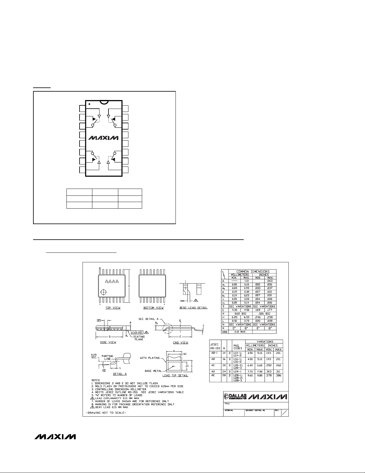
Pin Configurations (continued)
Package Information
(The package drawing(s) in this data sheet may not reflect the most current specifications. For the latest package outline information
go to www.maxim-ic.com/packages
.)
TOP VIEW
1
IN1
2
D1
S1
3
V-
4
MAX4613
5
GND
6
S4
7
D4
IN4
8
DIP/SO/QSOP/TSSOP
SW
LOGIC SW2, SW
0
1
1
OFF
ON
, SW
SWITCHES SHOWN FOR LOGIC "0" INPUT
16
IN2
D2
15
S2
14
13
V+
V
12
L
11
S3
10
D3
9
IN3
4
3
ON
OFF
TSSOP4.40mm.EPS
PACKAGE OUTLINE, TSSOP 4.40mm BODY
21-0066
1
I
1
Page 10

MAX4613
Quad, SPST Analog Switch
Maxim cannot assume responsibility for use of any circuitry other than circuitry entirely embodied in a Maxim product. No circuit patent licenses are
implied. Maxim reserves the right to change the circuitry and specifications without notice at any time.
10 ____________________Maxim Integrated Products, 120 San Gabriel Drive, Sunnyvale, CA 94086 408-737-7600
© 2007 Maxim Integrated Products is a registered trademark of Maxim Integrated Products.
Package Information (continued)
(The package drawing(s) in this data sheet may not reflect the most current specifications. For the latest package outline information
go to www.maxim-ic.com/packages
.)
QFN THIN.EPS
 Loading...