

MAX4610/MAX4611/MAX4612
Low-Voltage, Quad, SPST
CMOS Analog Switches
________________________________________________________________
Maxim Integrated Products
1
19-4793; Rev 6; 5/09
For pricing, delivery, and ordering information, please contact Maxim Direct at 1-888-629-4642,
or visit Maxim’s website at www.maxim-ic.com.
General Description
The MAX4610/MAX4611/MAX4612 are quad, low-voltage, single-pole/single-throw (SPST) analog switches.
On-resistance (100Ω, max) is matched between switches to 4Ω, max and is flat (4Ω, max) over the specified
signal range. Each switch handles V+ to GND analog
signal levels. Maximum off-leakage current is only 1nA
at TA= +25°C and 2nA at TA= +85°C.
The MAX4610 has four normally open (NO) switches,
and the MAX4611 has four normally closed (NC)
switches. The MAX4612 has two NO switches and two
NC switches. These CMOS switches operate from a
single +2V to +12V supply. All digital inputs have +0.8V
and +2.4V logic thresholds, ensuring TTL/CMOS-logic
compatibility when using a single +5V supply.
________________________Applications
Battery-Operated Equipment
Audio/Video Signal Routing
Low-Voltage Data-Acquisition Systems
Sample-and-Hold Circuits
Communication Circuits
____________________________Features
♦♦
Offered in Automotive Temperature Range
(-40°C to +125°C)
♦♦
Guaranteed On-Resistance
100Ω max (5V Supply)
46Ω max (12V Supply)
♦♦
Guaranteed Match Between Channels (4Ω, max)
♦♦
Guaranteed Flatness Over Signal Range (18Ω, max)
♦♦
Off-Leakage Current Over Temperature
< 2nA at T
A
= +85°C
♦♦
> 2kV ESD Protection per Method 3015.7
♦♦
Rail-to-Rail Signal Handling
♦♦
TTL/CMOS-Logic Compatible
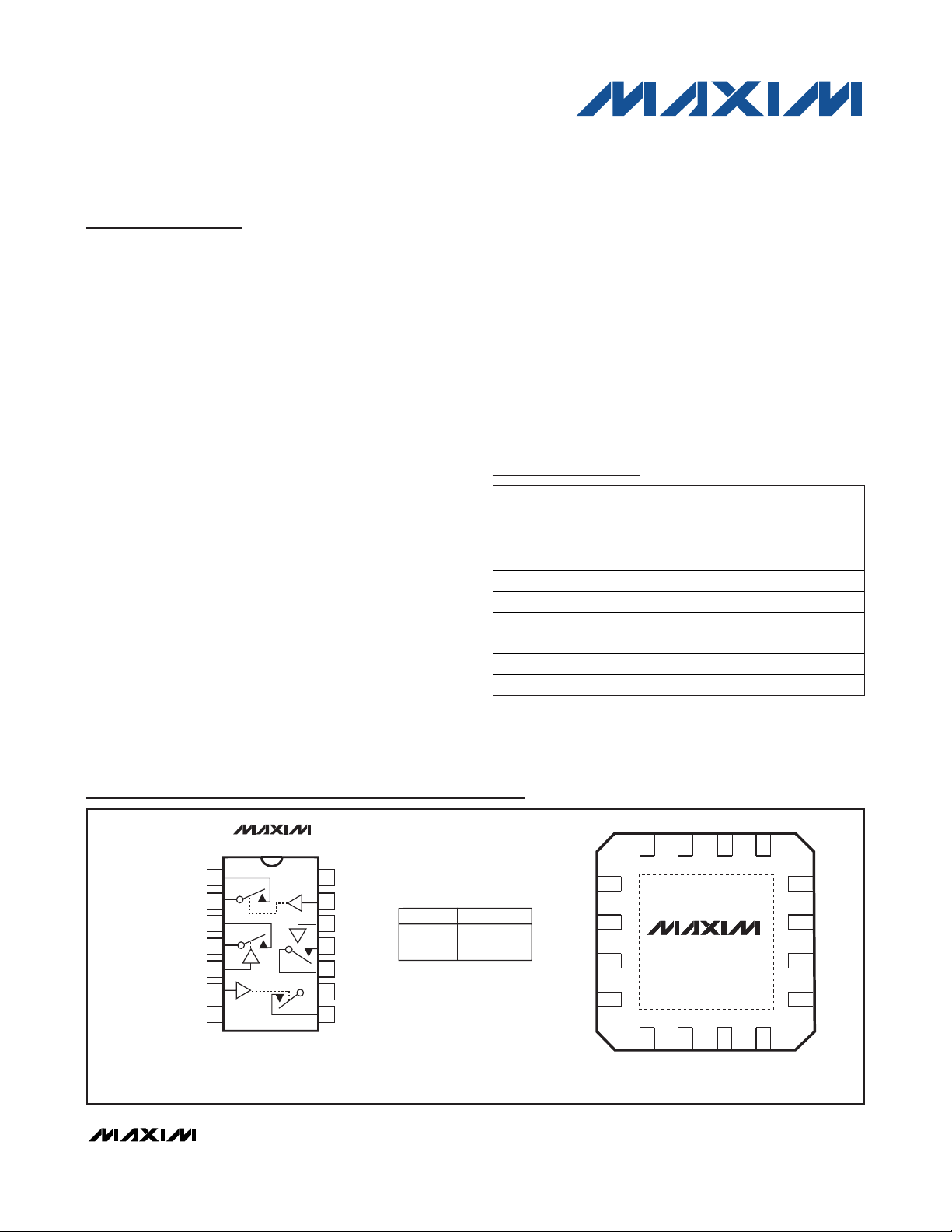
Pin Configurations/Truth Tables
Ordering Information
Ordering Information continued at end of data sheet.
*
Contact factory for dice specifications.
**
EP = Exposed pad.
+
Denotes a lead(Pb)-free/RoHS-compliant package.
MAX4611/MAX4612 Pin Configurations/Truth Tables appear at end of data sheet.
PART TEMP RANGE PIN-PACKAGE
MAX4610CUD+ 0°C to +70°C 14 TSSOP
MAX4610CSD+ 0°C to +70°C 14 Narrow SO
MAX4610CPD+ 0°C to +70°C 14 Plastic DIP
MAX4610C/D+ 0°C to +70°C Dice*
MAX4610EGE+ -40°C to +85°C 16 QFN-EP**
MAX4610EUD+ -40°C to +85°C 14 TSSOP
MAX4610ESD+ -40°C to +85°C 14 Narrow SO
MAX4610EPD+ -40°C to +85°C 14 Pla stic DIP
MAX4610ASD+ -40°C to +125°C 14 Narrow SO
TOP VIEW
NO1
COM1
NO2
COM2
IN2
IN3
GND
MAX4610
+
1
2
3
4
5
6
7
TSSOP/SO/DIP
14
V+
IN1
13
12
IN4
11
NO4
10
COM4
COM3
9
8
NO3
INPUT SWITCH STATE
LOW
HIGH
OFF
ON
IN1
+
1NO1
2COM1
3NO2
4
COM2
**EP = EXPOSED PAD
CONNECT EP TO V+
N.C.
16V+15
EP**
MAX4610
5
6
IN2
IN3
QFN
GND
IN4
14
13
12 N.C.
11 NO4
10 COM4
9
COM3
7
8
NO3
MAX4610/MAX4611/MAX4612
Low-Voltage, Quad, SPST
CMOS Analog Switches
2 _______________________________________________________________________________________
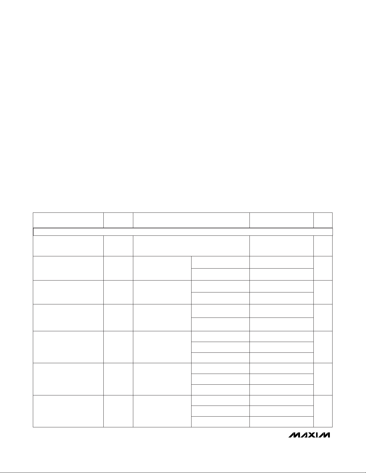
ABSOLUTE MAXIMUM RATINGS
ELECTRICAL CHARACTERISTICS—Single +5V Supply
(V+ = +5V ±10%, V
IN_H
= 2.4V, V
IN_L
= 0.8V, TA= T
MIN
to T
MAX
, unless otherwise noted.)
Stresses beyond those listed under “Absolute Maximum Ratings” may cause permanent damage to the device. These are stress ratings only, and functional
operation of the device at these or any other conditions beyond those indicated in the operational sections of the specifications is not implied. Exposure to
absolute maximum rating conditions for extended periods may affect device reliability.
(Voltages referenced to GND.)
V+ ...........................................................................-0.3V to +13V
IN_, COM_, NO_, NC_ (Note 1)....................-0.3V to (V+ + 0.3V)
Continuous Current (any terminal)
(pulsed at 1ms, 10% duty cycle) .....................................20mA
Peak Current (any terminal)
(pulsed at 1ms, 10% duty cycle) .....................................40mA
ESD per Method 3015.7......................................................> 2kV
Continuous Power Dissipation (T
A
= +70°C)
14-Pin TSSOP (derate 6.3mW/°C above +70°C) ..........500mW
14-Pin Narrow SO (derate 8.00mW/°C above +70°C) ..640mW
14-Pin Plastic DIP (derate 10.00mW/°C above +70°C) ..800mW
16-Pin QFN (derate 18.5mW/°C above +70°C) ..........1481mW
Operating Temperature Ranges
MAX461_C_ _ ......................................................0°C to +70°C
MAX461_E_ _....................................................-40°C to +85°C
MAX461_A_ _ .................................................-40°C to +125°C
Storage Temperature Range .............................-65°C to +160°C
Lead Temperature (soldering, 10s) .................................+300°C
V+ = 5.5V;
V
COM
_
= 1V, 4.5V;
V
NO_
= 4.5V, 1V
V+ = 4.5V,
I
COM
_
= 1mA,
V
NO
_
= V
NC
_
= 3V
V+ = 4.5V;
I
COM
_
= 1mA;
V
NO
_
= V
NC
_
= 3V,
2V, 1V
CONDITIONS
nA
I
NO(OFF)
NO_ or NC_ Off-Leakage
Current (Note 6)
-30 +30
-0.1 +0.1
Ω
28
R
FLAT(ON)
On-Resistance Flatness
(Note 5)
V0V+
V
COM
_
,
V
NO_,
V
NC
_
Analog Signal Range
(Note 3)
12 22
ΩΔR
ON
On-Resistance Match
Between Channels (Note 4)
1.0 5
70 100
UNITS
MIN TYP MAX
(Note 2)
SYMBOLPARAMETER
TA= +25°C
TA= +25°C
TA= +25°C
TA= T
MIN
to T
MAX
TA= +25°C
TA= -40°C to +125°C
V+ = 5.5V;
V
COM
_
= 1V, 4.5V;
V
NO
_
= V
NC
_
= 4.5V, 1V
TA= +25°C
nAI
COM(OFF)
COM_ Off-Leakage Current
(Note 6)
-30 +30
TA= -40°C to +125°C
-0.1 +0.1
V+ = 5.5V;
V
COM_
= 1V, 4.5V;
V
NO
_
= V
NC
_
= 1V, 4.5V,
or floating
nA
I
COM(ON)
COM_ On-Leakage Current
(Note 6)
TA= +25°C -0.2 +0.2
On-Resistance R
ON
Ω
V+ = 4.5V,
I
COM
_
= 1mA,
V
NO
_
= V
NC
_
= 3V
Note 1: Signals on NO_, NC_, COM_, or IN_ exceeding V+ or GND are clamped by internal diodes. Limit forward-diode current to
maximum current rating.
TA= T
MIN
to T
MAX
8
150TA= T
MIN
to T
MAX
-30 +30TA= -40°C to +125°C
-4 +4TA= -40°C to +85°C
-2 +2TA= -40°C to +85°C
-2 +2TA= -40°C to +85°C
ANALOG SWITCH
MAX4610/MAX4611/MAX4612
Low-Voltage, Quad, SPST
CMOS Analog Switches
_______________________________________________________________________________________ 3
ELECTRICAL CHARACTERISTICS—Single +5V Supply (continued)
(V+ = +5V ±10%, V
IN_H
= 2.4V, V
IN_L
= 0.8V, TA= T
MIN
to T
MAX
, unless otherwise noted.)
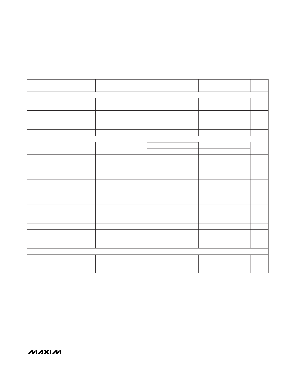
PARAMETER SYMBOL
MIN TYP MAX
(Note 2)
UNITS
Input Current with InputVoltage High
I
IN_H
-0.1 ±0.001 +0.1 µA
CONDITIONS
V
IN
_
= 2.4V, all others = 0.8V
Input Current with InputVoltage Low
I
IN_L
-0.1 ±0.001 +0.1 µAV
IN
_
= 0.8V, all others = 2.4V
Turn-On Time t
ON
35 65
ns
Charge Injection V
CTE
15pC
CL= 1.0nF, V
GEN
= 0,
R
GEN
= 0, Figure 3
TA= +25°C
TA= T
MIN
to T
MAX
90
V
COM
_
= 3V, Figure 2
TA= +25°C
TA= T
MIN
to T
MAX
30
V
COM
_
= 3V, Figure 2
Turn-Off Time t
OFF
15 28
ns
Power-Supply Range
Signal = 0dBm, Figure 4,
50Ω in and out
On-Channel Bandwidth BW 300 MHz
TA= +25°C
TA= +25°C
RL= 50Ω, CL= 5pF,
f = 1MHz, Figure 4
Off-Isolation (Note 7) V
ISO
-60 dB
TA= +25°C
RL= 50Ω, CL= 5pF,
f = 1MHz, Figure 5
Crosstalk (Note 8) V
CT
-80 dB
TA= +25°Cf = 1MHz, Figure 6NO_ or NC_ Capacitance C
(OFF)
16 pF
TA= +25°Cf = 1MHz, Figure 6COM_ Off-Capacitance C
COM(OFF)
16 pF
TA= +25°Cf = 1MHz, Figure 6COM_ On-Capacitance C
COM(ON)
pF
212V
Supply Current
23
I+
VIN= 0 or V+,
all switches on or off
-1 ±0.001 +1 µA
TA= +25°C
TA= +25°C
600Ω IN and OUT,
20Hz to 20kHz, 2V
P-P
Total Harmonic
Distortion
THD %0.009
Input High Voltage V
IN_H
2.4 1.5 V
Input Low Voltage V
IN_L
1.4 0.8 V
LOGIC INPUT
SUPPLY
DYNAMIC (Note 3)
MAX4610/MAX4611/MAX4612
Low-Voltage, Quad, SPST
CMOS Analog Switches
4 _______________________________________________________________________________________
ELECTRICAL CHARACTERISTICS—Single +3V Supply
(V+ = +3V, V
IN_H
= 2.4V, V
IN_L
= 0.5V, TA= T
MIN
to T
MAX
, unless otherwise noted.)
PARAMETER
Analog Signal Range
(Note 3)
SYMBOL
V
COM
_,
V
NO
_,
V
NC
_
CONDITIONS
MIN TYP MAX
(Note 2)
0V+
UNITS
V
On-Resistance R
ON
V+ = 2.7V,
I
COM
_
= 1mA,
V
NO
_
= V
NC
_
= 1V
175 360
Ω
-0.1 +0.1
-2 +2
NO_ or NC_ Off-Leakage
Current (Notes 3, 6)
I
NO(OFF)
V+ = 3.6V,
V
COM
_
= 0.5V, 3V;
V
NO
_
= V
NC
_
= 3V,
0.5V
-30 +30
nA
-0.2 +0.2
TA= +25°C
TA= T
MIN
to T
MAX
450
On-Resistance Match
Between Channels (Note 4)
ΔR
ON
V+ = 2.7V,
I
COM
_
= 1mA,
V
NO
_
= V
NC
_
= 1V
210
Ω
TA= +25°C
TA= T
MIN
to T
MAX
20
TA= +25°C
TA= -40°C to + 85°C
TA= -40°C to + 125°C
-4 +4
COM_ On-Leakage Current
(Notes 3, 6)
I
COM(ON)
V+ = 3.6V,
V
COM
_
= 0.5V, 3V;
V
NO
_
= V
NC
_
= 0.5V,
3V, or floating
-30 +30
nA
Input High Voltage V
IN_H
2.4 1.0 V
Input Low Voltage V
IN_L
1.0 0.5 V
TA=+25°C
TA= -40°C to + 85°C
-0.1 +0.1
TA= -40°C to + 125°C
-2 +2
COM_ Off-Leakage Current
(Notes 3, 6)
I
COM(OFF)
V+ = 3.6V,
V
COM
_
= 0.5V, 3V;
V
NO
_
= V
NC
_
= 3V,
0.5V
-30 +30
nA
TA= +25°C
TA= -40°C to +85°C
50 100
120
Turn-On Time t
ON
V
COM
_
= 1.5V,
Figure 2
140
ns
30 47
Turn-Off Time t
OFF
V
COM
_
= 1.5V,
Figure 2
60
ns
TA= +25°C
TA= -40°C to +85°C
TA= -40°C to +125°C
TA= -40°C to +125°C
TA= +25°C
TA= T
MIN
to T
MAX
ANALOG SWITCH
LOGIC INPUTS
DYNAMIC (Note 3)

MAX4610/MAX4611/MAX4612
Low-Voltage, Quad, SPST
CMOS Analog Switches
_______________________________________________________________________________________ 5
PARAMETER SYMBOL
MIN TYP MAX
(Note 2)
UNITS
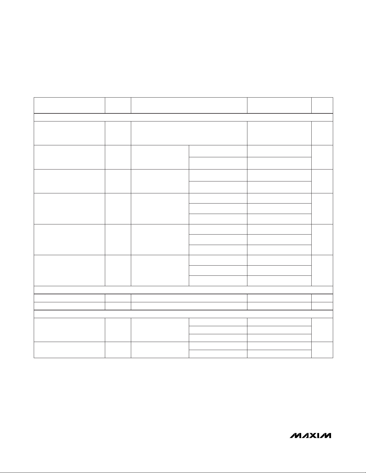
Analog Signal Range
(Note 3)
V
COM
_,
V
NO
_,
V
NC
_,
0V+V
CONDITIONS
On-Resistance R
ON
30 45
Ω
V+ = 12V,
I
COM
= 2mA,
V
NO_
= V
NC
_
= 10V
TA= +25°C
TA= T
MIN
to T
MAX
60
Note 2: The algebraic convention, where the most negative value is a minimum and the most positive value a maximum, is used in
this data sheet.
Note 3: Guaranteed by design.
Note 4: ΔR
ON
= RON(max) - RON(min).
Note 5: Flatness is defined as the difference between the maximum and minimum value of on-resistance as measured over the
specified analog signal range.
Note 6: Leakage parameters are 100% tested at maximum-rated hot temperature and guaranteed by correlation at +25°C.
Note 7: Off-Isolation = 20log
10(VCOM_
/ V
NO_
), V
COM_
= output, V
NO_
= input to off switch.
Note 8: Between any two switches.
ELECTRICAL CHARACTERISTICS—Single +12V Supply
(V+ = +12V, V
IN_H
= 4V, V
IN_L
= 0.8V, TA= T
MIN
to T
MAX
, unless otherwise noted.)
Input High Voltage V
IN_H
4.0 2.8 V
Input Low Voltage V
IN_L
2.5 0.8 V
Positive Supply Current I+ -1 ±0.001 +1 µAV
IN_
= 0 or V+, all switches on or off
ANALOG SWITCH
LOGIC INPUTS
SUPPLY

MAX4610/MAX4611/MAX4612
Low-Voltage, Quad, SPST
CMOS Analog Switches
6 _______________________________________________________________________________________
__________________________________________Typical Operating Characteristics
(TA = +25°C, unless otherwise noted.)
ON-RESISTANCE vs. V
80
70
60
(Ω)
50
ON
R
40
30
V+ = +12V
20
0681024 12
V+ = +5V
V+ = +9V
V
COM
(V)
COM
MAX4610-1A
(Ω)
ON
R
ON-RESISTANCE vs. V
400
350
300
250
200
150
100
50
034512 6
V+ = +2V
V+ = +3V
V
COM
COM
V+ = +5V
(V)
MAX4610-1B
90
80
70
(Ω)
60
ON
R
50
40
30
0 2.01.50.5 1.0 2.5 3.0 3.5 4.0 4.5 5.0
ON-RESISTANCE
vs. V
COM
AND TEMPERATURE
V+ = +5V
TA = +85°C
TA = +25°C
TA = -40°C
V
(V)
COM
MAX4610 toc02
OFF-LEAKAGE vs. TEMPERATURE
100
V+ = +5V
= 0
V
COM_
V
OR V
NC_
= +4.5V
NO_
10
1000
MAX4610-03
1
OFF-LEAKAGE (pA)
0.1
-40 -20 0 20 40 60 80 100
TEMPERATURE (°C)
CHARGE INJECTION vs. V
6
5
4
3
2
1
CHARGE INJECTION (pC)
0
-1
0462 8 10 12
V+ = +5V
V
COM_
(V)
COM
V+ = +12V
ON-LEAKAGE (pA)
0.01
MAX4610 toc06
GAIN (dB)
ON-LEAKAGE vs. TEMPERATURE
V+ = +5V
= 0
V
COM_
100
V
OR V
NO_
10
1
0.1
-40 -20 0 20 40 60 80 100
= FLOATING
NC_
TEMPERATURE (°C)
FREQUENCY RESPONSE
0
-10
-20
-30
-40
-50
-60
-70
-80
-90
-100
LOSS
PHASE
OFF-ISOLATION
10k1k 100k 1M 10M 100M 500M
FREQUENCY (Hz)
MAX4610 toc07
MAX4610-04
180
144
108
72
36
0
-36
-72
-108
-144
-180
10
1
0.1
I+ (pA)
0.01
0.001
-40 -20 0 20 40 60 80 100
TOTAL HARMONIC DISTORTION PLUS NOISE
1
0.1
THD + N (%)
PHASE (DEGREES)
0.01
0.001
10 100 1k 10k 100k 1M
SUPPLY CURRENT vs. TEMPERATURE
V+ = +5V
MAX4610-05
TEMPERATURE (°C)
vs. FREQUENCY
600Ω IN AND OUT
MAX4610-08
V+ = +2V, 1Vp-p SIGNAL
V+ = +3V, 1Vp-p SIGNAL
V+ = +5V, 2Vp-p SIGNAL
FREQUENCY (Hz)

Applications Information
Power-Supply Sequencing
and Overvoltage Protection
Do not exceed the absolute maximum ratings, because
stresses beyond the listed ratings may cause permanent
damage to the devices.
Proper power-supply sequencing is recommended for all
CMOS devices. Always apply V+ before applying analog
signals or logic inputs, especially if the analog or logic
signals are not current limited. If this sequencing is not
possible, and if the analog or logic inputs are not current
limited to 20mA, add a small-signal diode (D1) as shown
in Figure 1. If the analog signal can dip below GND, add
D2. Adding protection diodes reduces the analog signal
range to a diode drop (about 0.7V) below V+ (for D1),
and to a diode drop above ground (for D2). Leakage is
unaffected by adding the diodes. On-resistance increases by a small amount at low supply voltages. Maximum
supply voltage (V+) must not exceed 13V.
Adding protection diodes causes the logic thresholds to
be shifted relative to the power-supply rails. This can be
significant when low supply voltages (+5V or less) are
used. With a +5V supply, TTL compatibility is not guaranteed when protection diodes are added. Driving IN1
and IN2 all the way to the supply rails (i.e., to a diode
drop higher than the V+ pin, or to a diode drop lower
than the GND pin) is always acceptable.
MAX4610/MAX4611/MAX4612
Low-Voltage, Quad, SPST
CMOS Analog Switches
_______________________________________________________________________________________ 7
Figure 1. Overvoltage Protection Using Two External Blocking
Diodes
Pin Description
PIN
MAX4 610 MAX 4611 MAX4612
TSSOP/SO/ DIP QFN TSSOP/SO/DI P QFN TSSOP/ SO/DI P QFN
NAME FUNCTION
1, 3, 8, 11
1, 3,
8, 11
— — — — NO1–NO4
Analog Switch Normally Open
Terminal s
— — 1, 3, 8, 11
1, 3,
8, 11
— — NC1–NC4
Analog Switch Normally Closed
Terminal s
— — — — 1, 8 1, 8 NO1, NO3
Analog Switch Normally Open
Terminal s
— — — — 3, 11 3, 11 NC2, NC4
Analog Switch Normally Closed
Terminal s
2, 4, 9, 10
2, 4,
9, 10
2, 4, 9, 10
2, 4,
9, 10
2, 4, 9, 10
2, 4,
9, 10
COM1 –COM4
Analog Switch Common
Terminal s
13, 5, 6, 12
14, 5,
6, 13
13, 5, 6, 12
14, 5,
6, 13
13, 5, 6, 12
14, 5,
6, 13
IN1–IN4 Logic-Control Digital Input
7 7 7 7 7 7 GND
Ground. Connect to digital
ground.
— 12, 15 — 12, 15 — 12, 15 N.C.
No Connection. Not internally
connected.
14 16 14 16 14 16 V+
Positive Analog and DigitalSupply Voltage Input. Internally
connected to substrate.
— — — — — — EP
Exposed Pad (QFN only).
Connect to V+.
POSITIVE SUPPLY
V
g
NO_
V+
MAX4610
MAX4611
MAX4612
COM_

MAX4610/MAX4611/MAX4612
Low-Voltage, Quad, SPST
CMOS Analog Switches
8 _______________________________________________________________________________________
Figure 2. Switching Time
Figure 3. Charge Injection
______________________________________________Test Circuits/Timing Diagrams
Protection diodes D1 and D2 also protect against some
overvoltage situations. With Figure 1’s circuit, if the supply voltage is below the absolute maximum rating, and
if a fault voltage up to the absolute maximum rating is
applied to an analog signal pin, no damage will result.
Operating Considerations for
High-Voltage Supply
The MAX4610/MAX4611/MAX4612 are pin-compatible
with the industry-standard 74HC4066 and the
MAX4066, and are optimized for +5V single-supply
operation. The MAX4610 family is capable of +12V
single-supply operation with some precautions. The
absolute maximum rating for V+ is +13.2V (referenced
to GND). When operating near this region, bypass V+
with a minimum 0.1µF capacitor to ground as close to
the IC as possible.
Caution: The absolute maximum V+ to V- differential
voltage is 13.0V. Typical ±6V or 12V supplies with
±10% tolerances can be as high as 13.2V. This voltage can damage the MAX4610/MAX4611/MAX4612.
Even ±5% tolerance supplies may have overshoot or
noise spikes that exceed 13.0V.
MAX4610
MAX4611
MAX4612
SWITCH
INPUT
LOGIC
INPUT
V
COM
COM_
_
IN_
GND
V+
V+
NO_, NC_
R
L
300Ω
SWITCH
OUTPUT
C
L
35pF
t
OFF
tR < 20ns
t
< 20ns
F
0.9 · V
OUT
V
INH
LOGIC
V
OUT
INPUT
SWITCH
OUTPUT
0V
0V
50% 50%
V
OUT
0.9 · V
0UT
t
ON
INCLUDES FIXTURE AND STRAY CAPACITANCE.
C
L
V
OUT
RL + R
= V
COM (
R
L
)
ON
MAX4610
MAX4611
MAX4612
V
GEN
R
GEN
COM_
GND
IN_
V
V+
V+
NO_, NC_
IN
V
OUT
V
OUT
C
L
OFF
IN
Q = (ΔV
ON
OUT
)(CL)
ΔV
OUT
OFF

MAX4610/MAX4611/MAX4612
Low-Voltage, Quad, SPST
CMOS Analog Switches
_______________________________________________________________________________________ 9
Figure 4. Off-Isolation/On-Channel Bandwidth
Figure 5. Crosstalk
Figure 6. Channel Off/On-Capacitance
Test Circuits/Timing Diagrams (continued)
*
Contact factory for dice specifications.
**
EP = Exposed pad.
+
Denotes a lead(Pb)-free/RoHS-compliant package.
PART TEMP RANGE PIN-PACKAGE
MAX4611CUD+ 0°C to +70°C 14 TSSOP
MAX4611CSD+ 0°C to +70°C 14 Narrow SO
MAX4611CPD+ 0°C to +70°C 14 Plastic DIP
MAX4611C/D+ 0°C to +70°C Dice*
MAX4611EGE+ -40°C to +85°C 16 QFN-EP**
MAX4611EUD+ -40°C to +85°C 14 TSSOP
MAX4611ESD+ -40°C to +85°C 14 Narrow SO
MAX4611EPD+ -40°C to +85°C 14 Pla stic DIP
MAX4611AUD+ -40°C to +85°C 14 TSSOP
MAX4611ASD+ -40°C to +85°C 14 Narrow SO
MAX4612CUD+ 0°C to +70°C 14 TSSOP
MAX4612CSD+ 0°C to +70°C 14 Narrow SO
MAX4612CPD+ 0°C to +70°C 14 Plastic DIP
MAX4612C/D+ 0°C to +70°C Dice*
MAX4612EUD+ -40°C to +85°C 14 TSSOP
MAX4612ESD+ -40°C to +85°C 14 Narrow SO
MAX4612EGE+ -40°C to +85°C 16 QFN-EP**
MAX4612EPD+ -40°C to +85°C 14 Pla stic DIP
MAX4612AUD+ -40°C to +125°C 14 TSSOP
MAX4612ASD+ -40°C to +125°C 14 Narrow SO
Ordering Information (continued)
V+
10nF
SIGNAL
GENERATOR 0dBm
ANALYZER
R
L
V+
COM_
NO_, NC_
GND
V+
10nF
V+
COM_
MAX4610
MAX4611
MAX4612
IN_
MAX4610
10nF
V+
MAX4611
MAX4612
SIGNAL
GENERATOR 0dBm
V
OR
IN_L
V
IN_H
ANALYZER
V
OR
INL
V
INH
R
L
COM1
IN1
NO2
V+
GND
NO1
IN2
COM2
V
INL
V
MAX4610
MAX4611
MAX4612
50Ω
OR
INH
CAPACITANCE
METER
f = 1MHz
NO_, NC_
GND
IN_
V
OR
INL
V
INH

MAX4610/MAX4611/MAX4612
Low-Voltage, Quad, SPST
CMOS Analog Switches
10 ______________________________________________________________________________________
Pin Configurations/Truth Tables (continued)
PACKAGE TYPE PACKAGE CODE DOCUMENT NO.
14 TSSOP U14+1
21-0066
14 Narrow SO S14+2
21-0041
14 PDIP P14+6
21-0043
16 QFN G1644-1
21-0091
Package Information
For the latest package outline information, go to www.maxim-ic.com/packages.
TOP VIEW
NC1
COM1
NC2
COM2
IN2
IN3
GND
MAX4611
+
1
2
3
4
5
6
7
14
V+
IN1
13
12
IN4
11
NC4
10
COM4
COM3
9
8
NC3
INPUT SWITCH STATE
LOW
HIGH
ON
OFF
TSSOP/SO/DIP
TOP VIEW
NO1
COM1
NO2
COM2
IN2
IN3
GND
MAX4612
+
1
2
3
4
5
6
7
14
V+
IN1
13
12
IN4
11
NC4
10
COM4
COM3
9
8
NC3
INPUT NO1, NO2
LOW
HIGH
OFF
ON
NC3, NC4
ON
OFF
TSSOP/SO/DIP
V+
N.C.
+
16 15 14 13
NC1
1
EP**
COM1
2
NC2
3
COM2
4
**EP = EXPOSED PAD, CONNECT EP TO V+
NO1
COM1
NC2
COM2
**EP = EXPOSED PAD, CONNECT EP TO V+
MAX4611
6
5
IN2
IN3
V+
+
16 15 14 13
EP**
1
2
3
4
5
IN2
QFN
QFN
N.C.
MAX4612
IN3
IN1
7 8
GND
6
QFN
IN4
NC3
IN1
7 8
GND
NO3
N.C.
12
NC4
11
COM4
10
COM3
9
IN4
N.C.
12
NC4
11
COM4
10
COM3
9

Low-Voltage, Quad, SPST
CMOS Analog Switches
Maxim cannot assume responsibility for use of any circuitry other than circuitry entirely embodied in a Maxim product. No circuit patent licenses are
implied. Maxim reserves the right to change the circuitry and specifications without notice at any time.
Maxim Integrated Products, 120 San Gabriel Drive, Sunnyvale, CA 94086 408-737-7600 ____________________
11
© 2009 Maxim Integrated Products Maxim is a registered trademark of Maxim Integrated Products, Inc.
Revision History
REVISION
NUMBER
REVISION
DATE
DESCRIPTION
PAGES
CHANGED
0 1/99 -— —
6 5/09 Added lead-free packaging and added changes to EC table 1-4, 7, 9-13
 Loading...