

General Description
The MAX4580/MAX4590/MAX4600 dual analog switches
feature low on-resistance of 1.25Ω max. On-resistance is
matched between switches to 0.25Ω max and is flat
(0.3Ω max) over the specified signal range. Each switch
can handle Rail-to-Rail®analog signals. The off-leakage
current is only 2.5nA max at +85°C. These analog
switches are ideal in low-distortion applications and are
the preferred solution over mechanical relays in automatic test equipment or applications where current switching
is required. They have low power requirements, require
less board space, and are more reliable than mechanical
relays.
The MAX4580 has two NC (normally closed) switches,
the MAX4590 has two NO (normally open) switches,
and the MAX4600 has one NC (normally closed) and
one NO (normally open) switch.
These switches operate from a +4.5V to +36V single
supply or from ±4.5V to ±20V dual supplies. All digital
inputs have +0.8V and +2.4V logic thresholds, ensuring
TTL/CMOS-logic compatibility when using a +12V single supply or ±15V dual supplies.
Applications
Reed Relay Replacement
Test Equipment
Communication Systems
PBX, PABX Systems
Features
♦ Low On-Resistance (1.25Ω max)
♦ Guaranteed R
ON
Match Between Channels
(0.25Ω max)
♦ Guaranteed R
ON
Flatness Over Specified
Signal Range (0.3Ω max)
♦ Rail-to-Rail Signal Handling
♦ Guaranteed ESD Protection >2kV per
Method 3015.7
♦ Single-Supply Operation: +4.5V to +36V
Dual-Supply Operation: ±4.5V to ±20V
♦ TTL/CMOS-Compatible Control Inputs
MAX4580/MAX4590/MAX4600
1.25Ω, Dual SPST,
CMOS Analog Switches
________________________________________________________________ Maxim Integrated Products 1
19-1394; Rev 1; 6/03
PART
MAX4580CAE
MAX4580CWE
MAX4580CPE 0°C to +70°C
0°C to +70°C
0°C to +70°C
TEMP RANGE PIN-PACKAGE
16 SSOP
16 Wide SO
16 Plastic DIP
Ordering Information continued at end of data sheet.
Rail-to-Rail is a registered trademark of Nippon Motorola, Ltd.
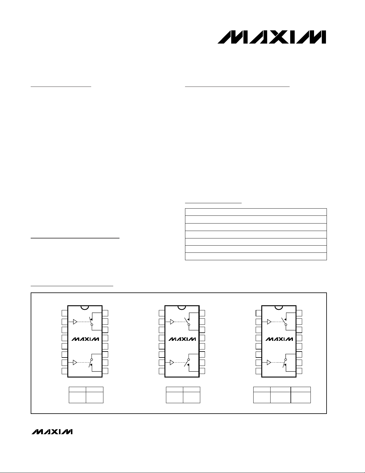
Pin Configurations/Functional Diagrams/Truth Tables
Ordering Information
MAX4580EAE -40°C to +85°C 16 SSOP
MAX4580EWE -40°C to +85°C 16 Wide SO
MAX4580EPE -40°C to +85°C 16 Plastic DIP
For pricing, delivery, and ordering information, please contact Maxim/Dallas Direct! at
1-888-629-4642, or visit Maxim’s website at www.maxim-ic.com.
TOP VIEW
N.C.
IN1
N.C.
GND
N.C.
IN2
N.C.
1
2
3
V-
4
MAX4580
5
6
7
8
NC1
16
N.C.
15
COM1
14
V+
13
V
12
L
COM2
11
N.C.
10
NC2
9
SSOP/SO/DIP
LOGIC SWITCH
0
ON
1
OFF
N.C. = NOT INTERNALLY CONNECTED
N.C.
IN1
N.C.
V-
GND
N.C.
IN2
N.C.
1
2
3
4
MAX4590
5
6
7
8
SSOP/SO/DIP
LOGIC SWITCH
0
1
OFF
ON
N01
16
N.C.
15
COM1
14
V+
13
V
12
L
COM2
11
N.C.
10
NO2
9
N.C.
IN1
N.C.
GND
N.C.
IN2
N.C.
1
2
3
V-
4
MAX4600
5
6
7
8
16
15
14
13
12
11
10
9
SSOP/SO/DIP
LOGIC SWITCH 1
0
1
OFF
ON
SWITCH 2
OFF
N01
N.C.
COM1
V+
V
L
COM2
N.C.
NC1
ON
MAX4580/MAX4590/MAX4600
1.25Ω, Dual SPST,
CMOS Analog Switches
2 _______________________________________________________________________________________
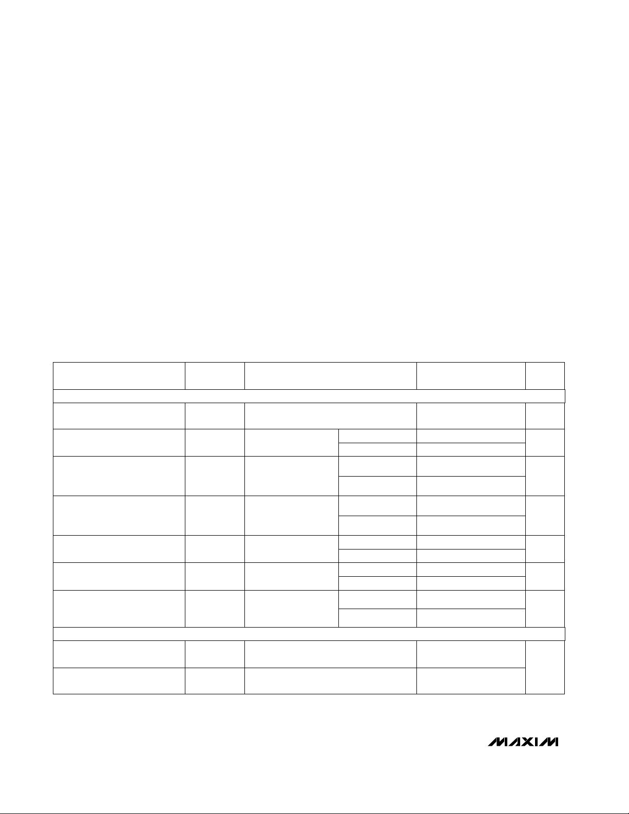
ABSOLUTE MAXIMUM RATINGS
Stresses beyond those listed under “Absolute Maximum Ratings” may cause permanent damage to the device. These are stress ratings only, and functional
operation of the device at these or any other conditions beyond those indicated in the operational sections of the specifications is not implied. Exposure to
absolute maximum rating conditions for extended periods may affect device reliability.
V+ to GND ..............................................................-0.3V to +44V
V- to GND ...............................................................+0.3V to -44V
V+ to V-...................................................................-0.3V to +44V
V
L
to GND.................................................... -0.3V to (V+ + 0.3V)
All Other Pins to GND (Note 1) ........... (V- - 0.3V) to (V+ + 0.3V)
Continuous Current (COM_, NO_, NC_) ....................... ±200mA
Peak Current (COM_, NO_, NC_)
(pulsed at 1ms, 10% duty cycle) .............................. ±300mA
Continuous Power Dissipation (T
A
= +70°C)
16 SSOP (derate 7.1mW/°C above +70°C) .................571mW
16 Wide SO (derate 9.52mW/°C above +70°C) ..........762mW
16 Plastic DIP (derate 10.53mW/°C above +70°C) .....842mW
Operating Temperature Ranges
MAX4_ _0C_E ....................................................0°C to +70°C
MAX4_ _0E_E ..................................................-40°C to +85°C
Storage Temperature Range ........................... -65°C to +160°C
Lead Temperature (soldering, 10sec) ............................+300°C
-2.5 2.5
-2.5 2.5
-5 5
TA= T
MIN
to T
MAX
V
TA= +25°C
V- V+
V
COM_,VNO_,
V
NC_
Input Voltage Range
(Note 3)
IN_ = 0.8V, all others = 2.4V
IN_ = 2.4V, all others = 0.8V
I
COM_
= 10mA,
V
NO_
or V
NC_
= ±10V,
TA= +25°C
TA= +25°C
TA= +25°C
CONDITIONS
Ω
0.05 0.25
∆R
ON
COM_ to NO_ or NC_
On-Resistance Match Between
Channels (Note 4)
Ω
0.9 1.25
R
ON
COM_ to NO or NC_
On-Resistance
-0.500 0.001 0.500
I
IN_L
Input Current with Input Voltage
Low
µA
-0.500 0.001 0.500
I
IN_H
Input Current with Input Voltage
High
Ω
0.06 0.3
R
FLAT(ON)
COM_ to NO_ or NC_
On-Resistance Flatness
(Note 5)
nA
-0.5 0.01 0.5
I
NO_,INC_
Off-Leakage Current
(NO_ or NC_) (Note 6)
nA
-0.5 0.01 0.5
I
COM_(OFF)
COM_ Off-Leakage Current
(Note 6)
nA
-1 0.01 1
I
COM_(ON)
COM_ On-Leakage Current
(Note 6)
UNITS
MIN TYP MAX
(Note 2)
SYMBOLPARAMETER
I
COM_
= 10mA,
V
NO_
or V
NC_
= ±10V
I
COM_
= 10mA; V
NO_
or V
NC_
= -5V, 0, +5V
TA= +25°C
V
COM_
= ±10V,
V
NO_
or V
NC_
= –+10V
V
COM_
= ±10V,
V
NO_
or V
NC_
= –+10V
V
COM_
= ±10V,
V
NO_
or V
NC_
= ±10V,
or floating
TA= +25°C
TA= T
MIN
to T
MAX
1.5
0.5
TA= T
MIN
to T
MAX
0.5
TA= T
MIN
to T
MAX
TA= T
MIN
to T
MAX
TA= T
MIN
to T
MAX
ELECTRICAL CHARACTERISTICS–Dual Supplies
(V+ = +15V, V- = -15V, VL= +5V, V
IN_H
= +2.4V, V
IN_L
= +0.8V, TA = T
MIN
to T
MAX
, unless otherwise noted. Typical values are at
TA= +25°C.)
Note 1: Signals on NC_, NO_, COM_, or IN_ exceeding V+ or V- are clamped by internal diodes. Limit forward diode current to
maximum current rating.
ANALOG SWITCH
LOGIC INPUT
MAX4580/MAX4590/MAX4600
1.25Ω, Dual SPST,
CMOS Analog Switches
_______________________________________________________________________________________ 3
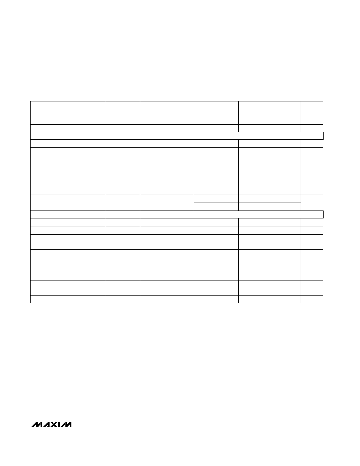
TA= T
MIN
to T
MAX
V
IN_
= 0 or +5V µA
TA= +25°C
-0.5 0.01 0.5
I+Positive Supply Current
TA= +25°C
f = 1MHz, Figure 6, TA= +25°C
RL= 50Ω, CL = 5pF, f = 1MHz,
Figure 5, T
A
= +25°C
TA= T
MIN
to T
MAX
55
RL= 50Ω, CL = 5pF, f = 1MHz,
Figure 4, TA= +25°C
CL = 1.0nF, V
GEN
= 0, R
GEN
= 0,
Figure 3, TA= +25°C
V
IN_
= 0 or +5V
TA= +25°C
f = 1MHz, Figure 6, TA= +25°C
CONDITIONS
pF
dB
f = 1MHz, Figure 7, TA= +25°C pF520C
(COM)
On-Capacitance
115C
(COM)
COM Off-Capacitance
-0.5 0.01 0.5
I
L
Logic Supply Current
-0.5 0.01 0.5
I-Negative Supply Current
pF115C
(OFF)
NC_ or NO_ Capacitance
-65V
CT
Crosstalk (Note 8)
dB-53V
ISO
Off-Isolation (Note 7)
pC-60QCharge Injection
-0.5 0.01 0.5
I
GND
Ground Current
ns
160
t
ON
Turn-On Time
ns
210
t
OFF
Turn-Off Time
UNITS
MIN TYP MAX
(Note 2)
SYMBOLPARAMETER
V
IN_
= 0 or +5V
V
IN_
= 0 or +5V
TA= +25°C
Figure 2, V
COM_
= ±10V, TA= +25°C
Figure 2, V
COM_
= ±10V, TA= +25°C
TA= T
MIN
to T
MAX
55
55
TA= T
MIN
to T
MAX
55
ELECTRICAL CHARACTERISTICS–Dual Supplies (continued)
(V+ = +15V, V- = -15V, VL= +5V, V
IN_H
= +2.4V, V
IN_L
= +0.8V, TA = T
MIN
to T
MAX
, unless otherwise noted. Typical values are at
T
A
= +25°C.)
µA
µA
µA
V2.4 1.7V
IN_H
Logic Input High Voltage
V1.7 0.8V
IN_L
Logic Input Low Voltage
V±4.5 ±20.0Power-Supply Range
POWER SUPPLY
SWITCH DYNAMIC CHARACTERISTICS
MAX4580/MAX4590/MAX4600
1.25Ω, Dual SPST,
CMOS Analog Switches
4 _______________________________________________________________________________________
-2.5 2.5
-2.5 2.5
-10 10
TA= T
MIN
to T
MAX
V
TA= +25°C
GND V+
V
COM_
, V
NO_
,
V
NC_
Input Voltage Range
(Note 3)
IN_ = 2.4V, all others = 0.8V
+4.5 +36.0
IN_ = 0.8V, all others = 2.4V
I
COM_
= 10mA,
V
NO_
or V
NC_
= +10V,
V+ = 12V
TA= +25°C
TA= +25°C
TA= +25°C
CONDITIONS
Power-Supply Range
V
IN_
= 0 or +5V
V
IN_
= 0 or +5V
-0.5 0.001 0.5
I
L
Logic Supply Current
µA
-0.5 0.001 0.5
I+Positive Supply Current
V
µA
V
IN_
= 0 or +5V
-0.5 0.001 0.5
I
GND
Ground Current µA
TA= +25°C
TA= +25°C
TA= T
MIN
to T
MAX
TA= +25°C
TA= T
MIN
to T
MAX
TA= T
MIN
to T
MAX
55
55
55
0.8V
IN_L
Logic Input Low Voltage
Ω
0.4
∆R
ON
COM_ to NO_ or NC_
On-Resistance Match Between
Channels (Note 4)
Ω
1.6 3
R
ON
COM_ to NO_ or NC_
On-Resistance
V2.4V
IN_H
Logic Input High Voltage
-0.500 0.001 0.500
I
IN_H
Input Current with Input Voltage
Low
µA
-0.500 0.001 0.500
I
IN_L
Input Current with Input Voltage
High
Ω
0.4
R
FLAT(ON)
COM_ to NO_ or NC_
On-Resistance Flatness
(Note 5)
nA
-0.5 0.01 0.5
I
NO_,INC_
Off-Leakage Current
(NO_ or NC_) (Notes 6, 9)
nA
-0.5 0.01 0.5
I
COM_(OFF)
COM_ Off-Leakage Current
(Notes 6, 9)
nA
-1 0.02 1
I
COM_(ON)
COM_ On-Leakage Current
(Notes 6, 9)
UNITS
MIN TYP MAX
(Note 2)
SYMBOLPARAMETER
I
COM_
= 10mA, V
NO_
or V
NC_
= +10V
I
COM_
= 10mA; V
NO_
or V
NC_
= +3V, +6V,
+9V
TA= +25°C
V
COM_
= 1V, +10V;
V
NO_
or V
NC_
= +10V,
+1V
V
NO_
or V
NC_
= +10V,
+1V; V
COM_
= +1V,
+10V
V
COM_
= +1V, +10V;
V
NO_
or V
NC_
= +1V,
+10V, or floating
TA= +25°C
TA= T
MIN
to T
MAX
3.5
0.5
TA= T
MIN
to T
MAX
0.5
TA= T
MIN
to T
MAX
TA= T
MIN
to T
MAX
TA= T
MIN
to T
MAX
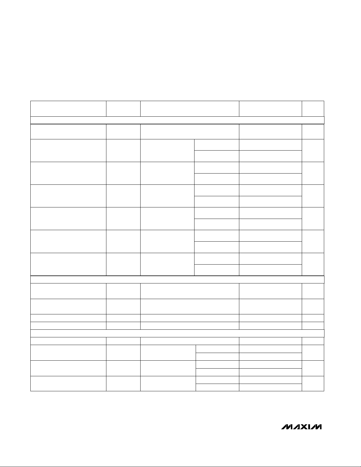
ELECTRICAL CHARACTERISTICS–Single Supply
(V+ = +12V, V- = 0, VL= +5V, V
INH
= 2.4V, V
INL
= 0.8V, TA= T
MIN
to T
MAX
, unless otherwise noted. Typical values are at
T
A
= +25°C.)
µA
V
ANALOG SWITCH
LOGIC INPUT
POWER SUPPLY

MAX4580/MAX4590/MAX4600
1.25Ω, Dual SPST,
CMOS Analog Switches
_______________________________________________________________________________________ 5
ELECTRICAL CHARACTERISTICS—Single Supply (continued)
(V+ = +12V, V- = 0, VL= +5V, V
IN_H
= 2.4V, V
IN_L
= 0.8V, TA = T
MIN
to T
MAX
, unless otherwise noted. Typical values are at
T
A
= +25°C.)
Note 2: The algebraic convention, where the most negative value is a minimum and the most positive value a maximum, is used in
this data sheet.
Note 3: Guaranteed by design.
Note 4: ∆R
ON
= R
ON(MAX)
- R
ON(MIN)
.
Note 5: Flatness is defined as the difference between the maximum and minimum value of on-resistance as measured over the
specified analog signal range.
Note 6: Leakage parameters are 100% tested at maximum-rated hot temperature and guaranteed by correlation at +25°C.
Note 7: Off-isolation = 20 log
10
[V
COM
/ (VNCor VNO)], V
COM
= output, VNCor VNO= input to off switch.
Note 8: Between any two switches.
Note 9: Leakage testing at single supply is guaranteed by testing with dual supplies.
RL= 50Ω, CL = 5pF, f = 1MHz,
Figure 5, TA= +25°C
CL = 1.0nF, V
GEN
= 0, R
GEN
= 0,
Figure 3, TA= +25°C
V
COM_
= +10V, Figure 2, TA= +25°C
PARAMETER SYMBOL
MIN TYP MAX
(Note 2)
UNITS
Crosstalk (Note 8) V
CT
-65
dB
Charge Injection Q
40
pC
Turn-Off Time t
OFF
200
ns
Turn-On Time t
ON
150
nsV
COM_
= +10V, Figure 2, TA= +25°C
f = 1MHz, Figure 7, TA= +25°COn-Capacitance C
(COM)_
275 pF
f = 1MHz, Figure 6, TA= +25°CCOM Off-Capacitance
CONDITIONS
C
(COM)_
175
f = 1MHz, Figure 6, TA= +25°CNC_ or NO_ Capacitance C
(OFF)_
175 pF
pF
SWITCH DYNAMIC CHARACTERISTICS
0
0.5
1.0
1.5
2.0
2.5
-20 -12 -8-16 -4 0 4 8 12 16 20
ON-RESISTANCE vs. V
COM
(DUAL SUPPLIES)
MAX4580 TOC01
V
COM
(V)
R
ON
(Ω)
V+, V- = ±5.0V
V+, V- = ±15.0V
V+, V- = ±20.0V
ON-RESISTANCE vs. V
COM
AND TEMPERATURE (DUAL SUPPLIES)
MAX4580 TOC02
V
COM
(V)
R
ON
(Ω)
129-12 -9 -6 0 3-3 6
0.5
0.6
0.7
0.8
0.9
1.0
1.1
1.2
0.4
-15 15
V+, V- = ±15V
TA = +85°C
TA = -40°C
TA = +25°C
ON-RESISTANCE vs. V
COM
(SINGLE SUPPLY)
MAX4580 TOC03
V
COM
(V)
R
ON
(Ω)
222018161412108642
1
2
3
4
5
0
024
V- = 0
V+ = +5V
V+ = +12V
V+ = +24V
Typical Operating Characteristics
(Circuit of Figure 1, TA = +25°C, unless otherwise noted.)

Typical Operating Characteristics (continued)
(Circuit of Figure 1, TA= +25°C, unless otherwise noted.)
MAX4580/MAX4590/MAX4600
1.25Ω, Dual SPST,
CMOS Analog Switches
6 _______________________________________________________________________________________
ON-RESISTANCE vs. V
COM
AND TEMPERATURE (SINGLE SUPPLY)
2.25
2.00
1.75
1.50
1.25
(Ω)
ON
R
1.00
0.75
0.50
0.25
0
012
TA = +85°C
TA = +25°C
TA = -40°C
V
(V)
COM
V+ = +12V
V- = GND
MAX4580 TOC04
11108 92 3 4 5 6 71
10
1
0.1
LEAKAGE (nA)
0.01
0.001
-40 0 20-20 40 60 80 100
vs. TEMPERATURE
V+ = +15V
V- = -15V
ON-LEAKAGE
ON/OFF-LEAKAGE
OFF-LEAKAGE
TEMPERATURE (°C)
POWER-SUPPLY CURRENT
vs. TEMPERATURE
10,000
1000
100
10
I+, I- (nA)
1
0.1
0.01
0.001
-40 0 20-20 40 60 80 100
I+
TEMPERATURE (°C)
I-
MAX4580 TOC07
CHARGE INJECTION
vs. V
500
400
MAX4580 TOC05
300
200
100
0
Q (pC)
-100
-200
-300
-400
-500
-15 -5 0-10 5 15
FREQUENCY RESPONSE
0
-10
-20
-30
-40
-50
LOSS (dB)
-60
-70
-80
-90
-100
0.01 1 100.1 100
ON-RESPONSE
ON-PHASE
OFF-ISOLATION
FREQUENCY (MHz)
V+ = +15V
V
MAX4580 TOC 08
V+, V- = 15V
INPUT = 0dBm
50Ω IN AND OUT
COM
V- = -15V
(V)
COM
V+ = +15V
V- = 0
+180
+90
0
-90
-180
-270
-360
-450
-540
-630
-720
MAX4580 TOC06
10
PHASE (degrees)
TURN-ON/TURN-OFF TIME
vs. TEMPERATURE
300
V
= +10V
COM
= 100Ω
R
L
= 35pF
C
250
L
200
(ns)
OFF
, t
ON
t
150
100
50
-40 10-15 35 60 85
TEMPERATURE (°C)
t
OFF
V+ = +15V
V- = -15V
t
ON
MAX4580 TOC09

MAX4580/MAX4590/MAX4600
1.25Ω, Dual SPST,
CMOS Analog Switches
_______________________________________________________________________________________ 7
Typical Operating Characteristics (continued)
(Circuit of Figure 1, TA= +25°C, unless otherwise noted.)
TURN-ON/TURN-OFF TIME vs. V
COM
MAX4580 TOC11
V
COM
(V)
t
ON
, t
OFF
(ns)
86420-2-4-6-8
120
140
160
180
200
220
100
-10 10
V+ = +15V
V- = -15V
R
L
= 100Ω
C
L
= 35pF
t
OFF
t
ON
Pin Description
NAME FUNCTION
MAX4580
12 V
L
Logic Supply Input
16, 9 NC1, NC2 Analog Switch Normally Closed Terminals
– NO1 Analog Switch Normally Open Terminal
– NC1 Analog Switch Normally Closed Terminal
– NO1, NO2 Analog Switch Normally Open Terminals
MAX4590
12
–
–
–
16, 9
MAX4600
PIN
12
–
16
9
–
IN1, IN2 Logic-Control Digital Inputs
1, 3, 6, 8,
10, 15
N.C.
No connection. Not internally connected. Connect to GND or lowimpedance point to improve on/off-isolation.
1, 3, 6, 8,
10, 15
1, 3, 6, 8,
10, 15
2, 7 2, 7 2, 7
5 GND Ground5 5
4 V-
Negative Analog Supply Voltage Input. Connect to GND for singlesupply operation.
4 4
14, 11 COM1, COM2 Analog Switch Common Terminals14, 11 14, 11
13 V+ Positive Analog Supply Input13 13
280
240
200
(ns)
OFF
, t
ON
t
160
120
80
TURN-ON/TURN-OFF TIME
vs. SUPPLY VOLTAGE
V+ = +15V
V- = -15V
10 1211 13 14 15 16 17 18 19 20
t
OFF
t
ON
V+, V- (V)
V
COM
R
C
= +10V
= 100Ω
L
= 35pF
L
MAX4580 TOC10

MAX4580/MAX4590/MAX4600
1.25Ω, Dual SPST,
CMOS Analog Switches
8 _______________________________________________________________________________________
___________Applications Information
Overvoltage Protection
Proper power-supply sequencing is recommended for
all CMOS devices. Do not exceed the absolute maximum ratings, because stresses beyond the listed ratings can cause permanent damage to the devices.
Always sequence V+ on first, then V-, followed by the
logic inputs, NO, or COM. If power-supply sequencing
is not possible, add two small signal diodes (D1, D2) in
series with supply pins for overvoltage protection
(Figure 1). Adding diodes reduces the analog signal
range to one diode drop below V+ and one diode drop
above V-, but does not affect the devices’ low switch
resistance and low leakage characteristics. Device
operation is unchanged, and the difference between V+
and V- should not exceed 44V. These protection diodes
are not recommended when using a single supply.
Figure 1. Overvoltage Protection Using External Blocking
Diodes
Figure 2. Switching-Time Test Circuit
+15V
D1
V+
MAX4580
MAX4590
MAX4600
*
COM_
*
V-
-15V
*
NO_
*
D2
* INTERNAL PROTECTION DIODES
+5V
V
L
COM_
IN_
GND
0
REPEAT TEST FOR EACH SWITCH. FOR LOAD
CONDITIONS, SEE Electrical Characteristics.
C
INCLUDES FIXTURE AND STRAY CAPACITANCE.
L
VO = V
( )
COM
LOGIC
INPUT
SWITCH
OUTPUT
+3V
0
V
O
0
50%
t
OFF
0.9V
0
t
ON
LOGIC INPUT WAVEFORMS INVERTED FOR SWITCHES
THAT HAVE THE OPPOSITE LOGIC SENSE.
tr < 20ns
tf < 20ns
0.9V
0
SWITCH
INPUT
LOGIC
INPUT
V
COM_
R
RL + R
+15V
V+
NO_
OR NC_
V-
-15V
L
ON
MAX4580
MAX4590
MAX4600
R
L
100Ω
SWITCH
OUTPUT
C
L
35pF
V
O

MAX4580/MAX4590/MAX4600
1.25Ω, Dual SPST,
CMOS Analog Switches
_______________________________________________________________________________________ 9
Figure 3. Charge-Injection Test Circuit
Figure 4. Off-Isolation Test Circuit
Figure 5. Crosstalk Test Circuit
MAX4580
MAX4590
MAX4600
V
GEN
R
GEN
+5V
V
COM_
GND
L
IN
+15V
V+
NC_ OR
NO_
V-
-15V
VIN = +3V
∆V
O
V
O
V
O
C
L
V
IN
OFF
OFF
V
IN
VIN DEPENDS ON SWITCH CONFIGURATION;
INPUT POLARITY DETERMINED BY SENSE OF SWITCH.
ON
ON
Q = (∆VO)(CL)
OFF
OFF
+15V
C
SIGNAL
GENERATOR 0dBm
COM_
ANALYZER
R
L
NC_ OR NO_
GND
+5V
MAX4580
MAX4590
C
+15V
+5V
MAX4600
V+
-15V
V
L
0 OR
IN_
V-
2.4V
C
SIGNAL
GENERATOR 0dBm
0 OR 2.4V
ANALYZER
R
L
COM1
IN1
N02
V+
GND
V
-15V
L
COM2
V-
N01
MAX4580
MAX4590
MAX4600
50Ω
IN2
0 OR
2.4V
NC
C

MAX4580/MAX4590/MAX4600
1.25Ω, Dual SPST,
CMOS Analog Switches
10 ______________________________________________________________________________________
Ordering Information (continued)
___________________
Chip Information
TRANSISTOR COUNT: 100
Figure 6. Switch Off-Capacitance Test Circuit
CAPACITANCE
METER
NC_ OR NO_
COM_
GND
C
V-
-15V
IN_
0 or
2.4V
C
+15V
V
L
+5V
f = 1MHz
V+
MAX4580
MAX4590
MAX4600
Figure 7. Switch On-Capacitance Test Circuit
PART
MAX4590CAE
MAX4590CWE
MAX4590CPE 0°C to +70°C
0°C to +70°C
0°C to +70°C
TEMP RANGE PIN-PACKAGE
16 SSOP
16 Wide SO
16 Plastic DIP
MAX4590EAE -40°C to +85°C 16 SSOP
MAX4590EWE -40°C to +85°C 16 Wide SO
MAX4590EPE -40°C to +85°C 16 Plastic DIP
MAX4600CAE
0°C to +70°C 16 SSOP
MAX4600CWE 0°C to +70°C 16 Wide SO
MAX4600CPE 0°C to +70°C 16 Plastic DIP
MAX4600EAE -40°C to +85°C 16 SSOP
MAX4600EWE -40°C to +85°C 16 Wide SO
MAX4600EPE -40°C to +85°C 16 Plastic DIP
MAX4580
+15V
C
+5V
MAX4590
MAX4600
V+
COM_
CAPACITANCE
METER
f = 1MHz
NC_ OR NO_
GND
V-
-15V
V
L
IN_
0 or
2.4V
C

MAX4580/MAX4590/MAX4600
1.25Ω, Dual SPST,
CMOS Analog Switches
______________________________________________________________________________________ 11
Package Information
(The package drawing(s) in this data sheet may not reflect the most current specifications. For the latest package outline information
go to www.maxim-ic.com/packages
.)
e
D
12
MAX
0.078
0.008
0.015
0.008
0.212
0.311
0.037
8∞
MILLIMETERS
MAX
MIN
1.73 1.99
0.21
0.05
0.38
0.25
0.20
0.09
5.38
5.20
0.65 BSC
7.90
7.65
0.63
0.95
0∞
8∞
MAX
0.249
0.249
0.289
0.328
0.407
MILLIMETERS
MAX
MIN
6.07
6.33
6.07
6.33
7.07
7.33
8.07
8.33
10.07
10.33
14L
16L
24L
28L
C
INCHES
MIN
D
0.239
D
0.239
D
0.278
D
0.317
0.397
D
INCHES
DIM
MIN
A
0.068
A1
0.002
B
0.010
C
HE
N
A
B
A1
D
E
e
H
L
0.004
SEE VARIATIONS
0.205
0.0256 BSC
0.301
0.025
0∞
L
SSOP.EPS
N
20L
NOTES:
1. D&E DO NOT INCLUDE MOLD FLASH.
2. MOLD FLASH OR PROTRUSIONS NOT TO EXCEED .15 MM (.006").
3. CONTROLLING DIMENSION: MILLIMETERS.
4. MEETS JEDEC MO150.
5. LEADS TO BE COPLANAR WITHIN 0.10 MM.
PROPRIETARY INFORMATION
TITLE:
PACKAGE OUTLINE, SSOP, 5.3 MM
21-0056
REV.DOCUMENT CONTROL NO.APPROVAL
1
C
1

MAX4580/MAX4590/MAX4600
1.25Ω, Dual SPST,
CMOS Analog Switches
SOICW.EPS
PACKAGE OUTLINE, .300" SOIC
1
1
21-0042
B
REV.DOCUMENT CONTROL NO.APPROVAL
PROPRIETARY INFORMATION
TITLE:
TOP VIEW
FRONT VIEW
MAX
0.012
0.104
0.019
0.299
0.013
INCHES
0.291
0.009
E
C
DIM
0.014
0.004
B
A1
MIN
0.093A
0.23
7.40 7.60
0.32
MILLIMETERS
0.10
0.35
2.35
MIN
0.49
0.30
MAX
2.65
0.050
0.016L
0.40 1.27
0.5120.496D
D
MINDIM
D
INCHES
MAX
12.60 13.00
MILLIMETERS
MIN
MAX
20 AC
0.447 0.463 AB11.7511.35 18
0.398 0.413 AA10.5010.10 16
N MS013
SIDE VIEW
H 0.4190.394 10.00 10.65
e 0.050 1.27
D 0.6140.598 15.20 2415.60 AD
D 0.7130.697 17.70 2818.10 AE
H
E
N
D
A1
B
e
A
0∞-8∞
C
L
1
VARIATIONS:
Package Information (continued)
(The package drawing(s) in this data sheet may not reflect the most current specifications. For the latest package outline information
go to www.maxim-ic.com/packages
.)
Maxim cannot assume responsibility for use of any circuitry other than circuitry entirely embodied in a Maxim product. No circuit patent licenses are
implied. Maxim reserves the right to change the circuitry and specifications without notice at any time.
12 ____________________Maxim Integrated Products, 120 San Gabriel Drive, Sunnyvale, CA 94086 408-737-7600
© 2003 Maxim Integrated Products Printed USA is a registered trademark of Maxim Integrated Products.
 Loading...