Maxim MAX459CQH, MAX459CPL, MAX458CQH, MAX458CPL, MAX459EPL Datasheet

19-0258; Rev 2; 4/95
EVALUATION KIT MANUAL
FOLLOWS DATA SHEET
8x4 Video Crosspoint Switches with Buffers
_______________General Description
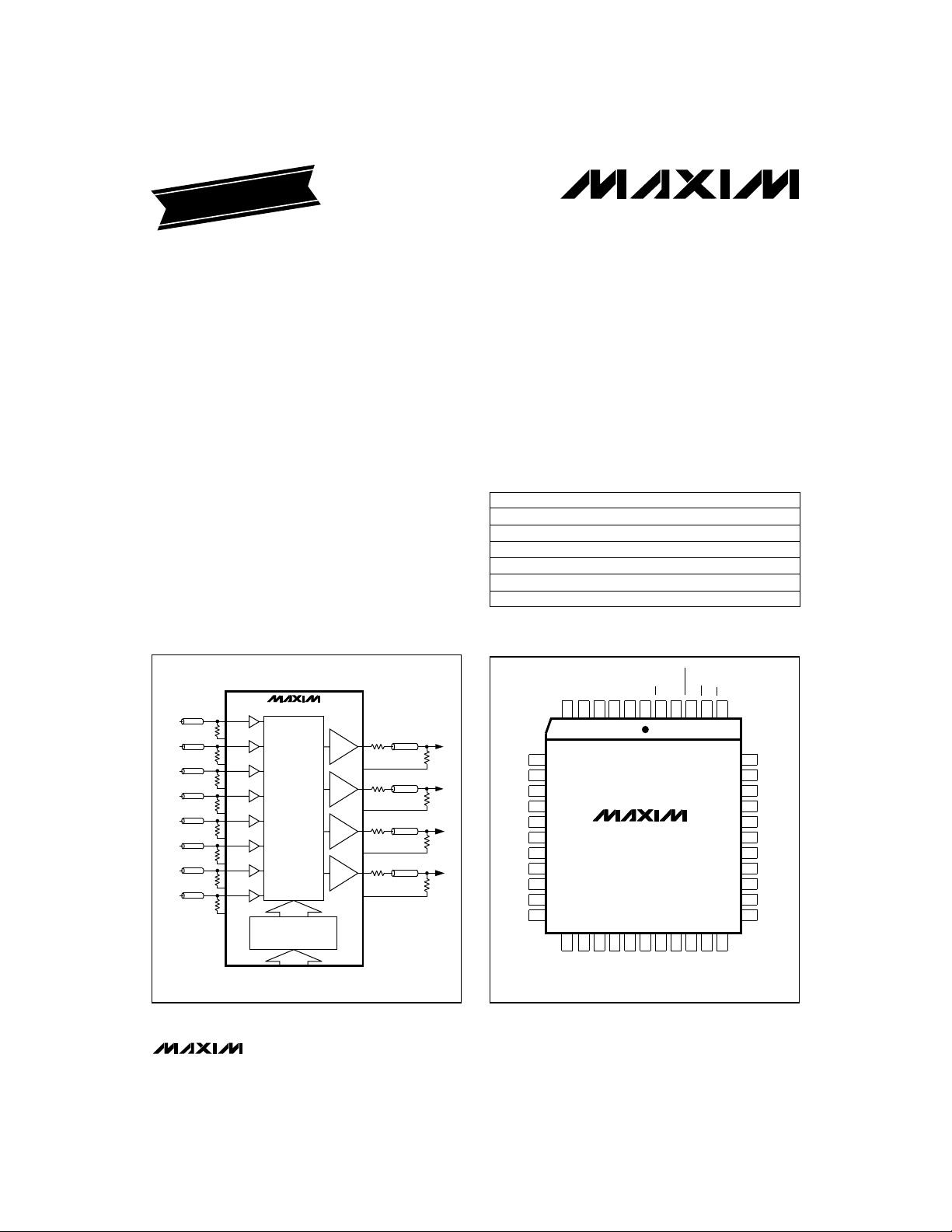
The MAX458/MAX459 are crosspoint switches with eight
input channels and four high-speed, buffered output
channels. The MAX458 output buffer is configured with a
gain of one, while the MAX459 buffer has a gain of two. In
each device, any one of eight input lines can be connected to any of four output amplifiers. The output buffers are
capable of driving loads of 75Ω.
Data interface can be accomplished by either a 16-bit
serial or a 6-bit parallel connection. In the serial mode,
the MAX458/MAX459 are SPITM, QSPITM, and Microwire
compatible. In parallel mode, the MAX458/MAX459 are
compatible with most microprocessor buses. Three-state
amplifier output capability makes it possible to multiplex
MAX458/MAX459s to form larger switch networks. The
output buffers can be disabled individually or the entire
device can be shut down to conserve power.
________________________Applications
Video Test Equipment
Video Security Systems
____________________________Features
♦ 100MHz Unity-Gain Bandwidth
♦ 300V/µs Slew Rate
♦ Low 0.05° Differential Phase Error
♦ Low 0.01% Differential Gain Error
♦ Directly Drives 75Ω Cables
♦ Fast 60ns Switching Time
♦ High-Z Amplifier Output Capability
♦ Shutdown Capability
♦ 16-Bit Serial and 6-Bit Parallel Address Modes
TM
♦ 40-Pin DIP and 44-Pin PLCC Packages
______________Ordering Information
PART
MAX458CPL
MAX458CQH
MAX458EPL -40°C to +85°C
MAX459CPL
MAX459CQH
MAX459EPL -40°C to +85°C
TEMP. RANGE PIN-PACKAGE
0°C to +70°C
0°C to +70°C
0°C to +70°C 40 Plastic DIP
0°C to +70°C
Video Editing
_____________________Block Diagram
8 BUFFERED
INPUTS
IN0
75Ω
IN1
IN2
IN3
IN4
IN5
IN6
IN7
™
SPI and QSPI are trademarks of Motorola, Inc. Microwire is a trademark of National Semiconductor Corp.
GND
75Ω
GND
75Ω
GND
75Ω
GND
75Ω
GND
75Ω
GND
75Ω
GND
75Ω
GND
(SPI™, QSPI™, MICROWIRE™ COMPATIBLE)
8 x 4
SWITCH ARRAY
SERIAL OR PARALLEL
DIGITAL INTERFACE
SERIAL/PARALLEL INTERFACE
MAX459
8 x 4
SWITCH
ARRAY
& CONTROL
OUTPUT DRIVERS
AV = 2
AV = 2
AV = 2
AV = 2
4 75Ω
GND
GND
GND
GND
75Ω
75Ω
75Ω
75Ω
OUT0
75Ω
OUT1
75Ω
OUT2
75Ω
OUT3
75Ω
_________________Pin Configurations
TOP VIEW
GND
IN0
GND
N.C.
MAX458
MAX459
21
22 2319
20
IN7
GND
DOUT
SHDN
PLCC
IN1
7
GND
8
IN2
9
10
GND
11
IN3
12
V
CC
13
IN4
14
V
EE
15
IN5
GND
16
IN6
17
DIP on last page.
N.C.
5
6
18
GND
40 Plastic DIP
44 PLCC
40 Plastic DIP
44 PLCC
40 Plastic DIP
DINCSSCLK
UPDATEWRCE
43
441234404142
25
26
24
D3D1D2A1D0
27
N.C.
MAX458/MAX459
39
GND
38
OUT0
37
GND
36
OUT1
35
V
CC
34
OUT2
33
V
EE
32
N.C.
31
OUT3
30
GND
29
A0
28
_______________________________________________________________
Maxim Integrated Products
Call toll free 1-800-998-8800 for free samples or literature.
1

8x4 Video Crosspoint Switches with Buffers
ABSOLUTE MAXIMUM RATINGS
Total Supply Voltage (VCCto VEE).........................................12V
Positive Supply Voltage (VCCto GND).....................................6V
Negative Supply Voltage (VEEto GND)...................................6V
Analog Input/Output Voltage ...........(VCC+ 0.3V) to (VEE- 0.3V)
Digital Input Voltage...................................(VCC+ 0.3V) to -0.3V
Duration of Output Short Circuit to GND (Note 1)......Continuous
Continuous Power Dissipation
Plastic DIP (derate 17mW/°C above +70°C) ..............1333mW
PLCC (derate 13mW/°C above +70°C) ......................1067mW
Note 1: Outputs may be shorted to any supply pin or ground as long as package power dissipation ratings are not exceeded.
Stresses beyond those listed under “Absolute Maximum Ratings” may cause permanent damage to the device. These are stress ratings only, and functional
operation of the device at these or any other conditions beyond those indicated in the operational sections of the specifications is not implied. Exposure to
absolute maximum rating conditions for extended periods may affect device reliability.
ELECTRICAL CHARACTERISTICS
(VCC= +5V, VEE= -5V, -2V ≤ VIN≤ +2V, output load resistor (RL) = 150Ω, TA= T
MAX458/MAX459
Typical values are at T
STATIC SPECIFICATIONS
Input Offset Voltage
Input Offset Voltage Match
On Input Bias Current
On Input Resistance
Input Capacitance
DC Voltage Gain Accuracy
Output Voltage Swing
Enabled Output Resistance
Disabled Output Resistance
Disabled Output Capacitance
Positive Power-Supply Current
Negative Power-Supply Current
Positive Supply Current in
Shutdown
Negative Supply Current in
Shutdown
Logic Input High Voltage
Logic Input Low Voltage
= +25°C.)
A
V
OS
OS
IN
IN
IN
OUT
R
OUT
R
OUT
OUT
I
CC
I
EE
IH
IL
Any channel
VIN= 0V (Note 2)
VS= ±4.75V to ±5.25V dB50 60PSRRPower-Supply Rejection Ratio
VIN= 0V, input programmed to one output
Input programmed to one output
Input channel on or off
MAX458 (Note 3)
MAX459 (Note 4)
VIN= 1kHz sine wave
VIN= 10MHz sine wave
MAX458
MAX459
VIN= 0V,
all amplifiers enabled
VIN= 0V,
all amplifiers enabled
(Note 5)
(Note 5)
Operating Temperature Ranges
MAX45_C_ _ ........................................................0°C to +70°C
MAX45_E_ _......................................................-40°C to +85°C
Junction Temperature......................................................+150°C
Storage Temperature Range.............................-65°C to +160°C
Lead Temperature (soldering, 10sec).............................+300°C
to T
MIN
, unless otherwise noted.
MAX
CONDITIONS
TA= +25°C
TA= T
MIN
TA= +25°C
TA= T
MIN
TA= +25°C
TA= T
MIN
to T
to T
to T
MAX
MAX
MAX
515
20
0.1 0.5
1.0
0.1 1.0
2.0
0.05
4.0
0.70 1.0
TA= +25°C
TA= T
MIN
TA= +25°C
TA= T
MIN
to T
to T
MAX
MAX
60 75 85
50 100
50 65 75
40 90
UNITSMIN TYP MAXSYMBOLPARAMETER
V-2 +2Input Voltage Range
mV
mV310∆V
µA±1 ±5I
MΩ0.50 5.0R
pF7C
%
V±2 ±3V
Ω
MΩ0.25 1.0
kΩ
pF12C
mA
mA
mA15 26
mA712
V2.0V
V0.8V
2 _______________________________________________________________________________________

8x4 Video Crosspoint Switches with Buffers
ELECTRICAL CHARACTERISTICS (continued)
(VCC= +5V, VEE= -5V, -2V ≤ VIN≤ +2V, output load resistor (RL) = 150Ω, TA= T
Typical values are at T
Logic Input High Current
Logic Input Low Current
Logic Output High Voltage
Logic Output Low Voltage
DYNAMIC SPECIFICATIONS
Input Noise Density
Settling Time
Amplifier Disable Time
Amplifier Enable Time
Channel Switching Time
Channel Switching Propagation Delay
Note 2: Defined as the DC offset shift when switching between input channels for a given output.
Note 3: Voltage Gain Accuracy for MAX458 calculated as (V
Note 4: Voltage Gain Accuracy for MAX459 calculated as (VOUT/2 - VIN) @ (VIN = +1V) - (VOUT/2 - VIN) @ (VIN = -1V)
Note 5: All logic levels are guaranteed over the range of VS= ±4.75V to ±5.25V.
Note 6: Differential phase and gain measured with a 40 IRE (285.7mV), 3.58MHz sine wave superimposed on a linear ramp of 0 IRE
Note 7: For MAX458, step input from +2V to 0V; for MAX459, step input from +1V to 0V. All unused channels grounded and all
Note 8: Test input channel programmed to an output and grounded through a 75Ω resistor. Adjacent input is programmed to an
Note 9: Same as Note 6 above, except driven input and output are not adjacent to test input/output.
Note 10: All inputs but the test input are driven by a 10MHz 4Vp-p sine wave. All outputs except the test output are connected to driven inputs.
Note 11: Same as Note 9 above, except with test channel programmed off.
to 100 IRE (714.3mV). “The IRE scale is a linear scale for measuring, in arbitrary IRE units, the relative amplitudes of the various components of a television signal” (from the “Television Engineering Handbook”, edited by K. Blair Benson, McGraw
Hill). This system defines 100 IRE as reference white, 0 IRE as the blanking level, and -40 IRE as the sync peak. The equipment used for the test signal generated 714.3mV (100 IRE) as reference white and -285.7mV (-40 IRE) as sync. The modulation used was 285.7mV (40 IRE), which conforms to the EIA color signal standards.
unused amplifiers disabled.
adjacent output and driven by a 10MHz, 4Vp-p sine wave.
= +25°C.)
A
IH
IL
OH
OL
DGDifferential Gain Error (Note 6)
DGDifferential Phase Error (Note 6)
SRSlew Rate
BWBandwidth (-3dB)
S
AOFF
AON
CSW
CPD
(Note 3)
(Note 3)
I
= 400µA (Note 5)
SOURCE
I
= 1.6mA (Note 5)
SINK
MAX458
MAX459
MAX458
MAX459
MAX458
MAX459
MAX458, RL= 75Ω
f = 10kHz
n
To 0.1% of final value (Note 7)
See
Typical Operating Characteristics
(Note 8)
(Note 9)
(Note 10)
(Note 11)
OUT - VIN) @ (VIN = +2V) - (VOUT - VIN) @ (VIN = -2V)
——————————––————————————4—V————————————————————
———————————————————————2—V——————————————————————
CONDITIONS
to T
MIN
MAX
Positive transition
Negative transition
Positive transition
Negative transition
, unless otherwise noted.
0.01
0.13
0.05
0.14
200
150
300
250
100
90MAX459, RL= 150Ω
100Switching Transient Glitch
UNITSMIN TYP MAXSYMBOLPARAMETER
µA10I
µA10I
V4.0V
V0.5V
%
degrees
V/µs
MHz
nV/√Hz20e
ns40t
ns100t
ns120t
ns60t
ns50t
mV
p-p
dB-65Adjacent Channel Crosstalk
dB-65Non-Adjacent Channel Crosstalk
dB-55All-Hostile Crosstalk
dB-60All-Hostile Off Isolation
MAX458/MAX459
_______________________________________________________________________________________ 3

8x4 Video Crosspoint Switches with Buffers
TIMING CHARACTERISTICS (Note 12)
(VCC= +5V, VEE= -5V, -2V ≤ VIN≤ +2V, output load resistor (RL) = 150Ω, TA= T
CONDITIONS
PARALLEL-MODE TIMING (see Figure 1)
Address to –W—R–Fall Setup Time
Address to –W—R–Rise Hold Time
–C—E–
Fall to –W—R–Fall Setup Time
–C—E–
Rise to –W—R–Rise Hold Time
–W—R–
Pulse Width Low
Data to –W—R–Rise Setup Time
Data to –W—R–Rise Hold Time
–W—R–
Rise to –U—P—D—A—T—E–Fall Setup Time
–U—P—D—A—T—E–
MAX458/MAX459
Pulse Width Low
–U—P—D—A—T—E–
Rise to –W—R–Fall Setup Time
ADS
ADH
CES
CEH
WR
DS
DH
WRS
UP
UPS
SERIAL-MODE TIMING (see Figure 6)
SCLK to –C—S–Fall
–C—S–
Fall to SCLK Rise
SCLK Pulse Width High
SCLK Pulse Width Low
DIN to SCLK Rise Setup Time
DIN to SCLK Rise Hold Time
SCLK Fall to DOUT
SCLK Rise to –C—S–Rise
–C—S–
Rise to SCLK Rise
–C—S–
Pulse Width High
CSO
CSS
CH
CL
DS
DH
DO
CSH
CS1
CSW
Note 12: Timing Characteristics are guaranteed by design.
MIN
to T
, unless otherwise noted.)
MAX
UNITSMIN MAXSYMBOLPARAMETER
ns20t
ns0t
ns0t
ns0t
ns40t
ns50t
ns0t
ns0t
ns40t
ns25t
ns0t
ns35t
ns50t
ns30t
ns50t
ns0t
ns200t
ns30t
ns20t
ns100t
4 _______________________________________________________________________________________

8x4 Video Crosspoint Switches with Buffers
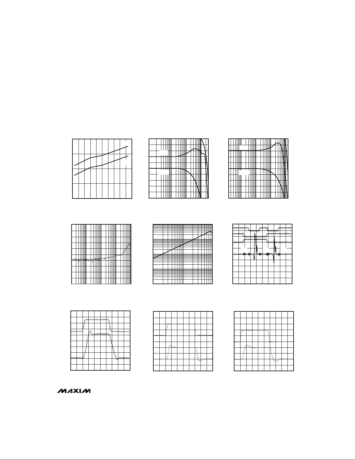
__________________________________________Typical Operating Characteristics
(TA = +25°C, unless otherwise noted.)
POWER SUPPLY CURRENT
vs. TEMPERATURE
100
80
60
CURRENT (mA)
40
20
-60 -40 -20 0 20 40 60 80 100 120 140
TEMPERATURE (°C)
CROSSTALK vs. FREQUENCY
40
0
-40
-80
AMPLITUDE (dB)
-120
I
CC
I
EE
6
4
2
MAX458/459 Fg TOC1
0
-2
-4
-6
AMPLITUDE (dB)
0.1 1 10 100 250
OUTPUT IMPEDANCE vs. FREQUENCY
MAX458/459 Fg TOC7
10
1
0.1
OUTPUT IMPEDANCE (Ω)
MAX458
GAIN vs. FREQUENCY
GAIN
PHASE
FREQUENCY (MHz)
6
MAX458/459 Fg TOC4
PHASE (DEGREES)
4
2
0
36
AMPLITUDE (dB)
72
108
144
180
UPDATE
MAX458/459 Fg TOC6
D0 & D2
GND
MAX459
GAIN vs. FREQUENCY
GAIN
PHASE
0.1 1 10 100 250
FREQUENCY (MHz)
CHANNEL SWITCH TRANSIENT
D1
OUT
MAX458/459 Fg TOC5
00
36
72
108
144
180
IN2IN5IN2
MAX458/MAX459
PHASE (DEGREES)
10V/div
(digital)
20mV/div
(analog)
0.01
0.1 10
FREQUENCY (MHz)
LARGE-SIGNAL PULSE RESPONSE
5V
2V/div
GND
1V/div
-15V
1 100
MAX458
25ns/div
+200mV
INPUT
-200mV
+100mV
OUTPUT
-100mV
MAX458/459 Fg TOC2
1 10 100
FREQUENCY (MHz)
MAX458
SMALL-SIGNAL PULSE RESPONSE
10ns/div
MAX458/459 Fg TOC8
+200mV
INPUT
-200mV
+200mV
OUTPUT
-200mV
100ns/div
MAX459
SMALL-SIGNAL PULSE RESPONSE
10ns/div
_______________________________________________________________________________________
MAX458/459 Fg TOC3
MAX458/459 Fg TOC9
INPUT
OUTPUT
5
 Loading...