

General Description
The MAX4599 single-pole/double-throw (SPDT) switch
operates from a +2.0V to +5.5V single supply. It offers
60Ω max on-resistance (RON) at +5V and fast switching
times (tON= 30ns max, t
OFF
= 25ns max).
The MAX4599 features excellent R
ON
flatness (4Ω max)
and matching (1Ω max) between channels. This device
also offers 5pC max charge injection.
The MAX4599 is available in tiny 6-pin SC70 and SOT23
packages.
Applications
Battery-Operated Equipment
Audio and Video Signal Routing
Cellular Phones
Low-Voltage Data-Acquisition Systems
Sample-and-Hold Circuits
Communications Circuits
Features
♦ Available in 6-Pin SC70 Package
♦ 60Ω max (40Ω typ) On-Resistance
♦ 1Ω max (0.2Ω typ) R
ON
Matching Between
Channels
♦ 4Ω max (2.5Ω typ) R
ON
Flatness
♦ Fast Switching: t
ON
= 30ns (max)
t
OFF
= 25ns (max)
♦ Guaranteed 5pC max Charge Injection
♦ +2.0V to +5.5V Single-Supply Operation
♦ 200MHz -3dB Bandwidth
♦ Low ±0.5nA Leakage Current at +25°C
♦ Break-Before-Make Switching
♦ TTL/CMOS-Logic Compatible
♦ -76dB Off-Isolation at 1MHz
♦ 0.12% Total Harmonic Distortion
MAX4599
Low-Voltage, Single-Supply,
SPDT Analog Switch in SC70
________________________________________________________________ Maxim Integrated Products 1
19-1637; Rev 0; 2/00
PART
MAX4599EXT-T
MAX4599EUT-T -40°C to +85°C
-40°C to +85°C
TEMP. RANGE
PIN-
PACKAGE
6 SC70-6
6 SOT23-6
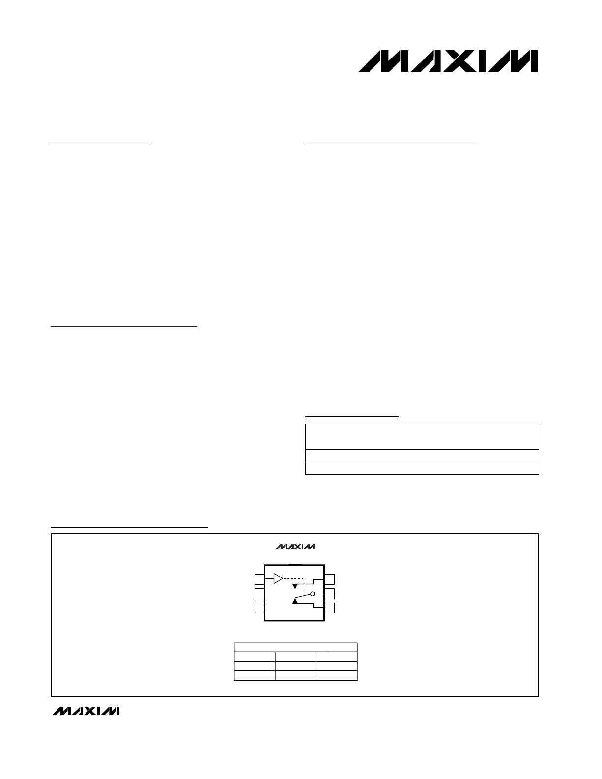
Pin Configuration/Functional Diagram/Truth Table
Ordering Information
TOP
MARK
AAF
AAHC
For free samples and the latest literature, visit www.maxim-ic.com or phone 1-800-998-8800.
For small orders, phone 1-800-835-8769.
MAX4599
16
IN
2
V+
GND
3
SC70-6/SOT23-6
IN
0
1 OFF
SWITCH IS SHOWN FOR "0" INPUT.
MAX4599
NC
ON
NO
5
COM
4
NC
NO
OFF
ON
MAX4599
Low-Voltage, Single-Supply,
SPDT Analog Switch in SC70
2 _______________________________________________________________________________________
ABSOLUTE MAXIMUM RATINGS
ELECTRICAL CHARACTERISTICS— Single +5V Supply
(V+ = +4.5V to +5.5V, V
INH
= +2.4V, V
INL
= +0.8V, TA= T
MIN
to T
MAX
, unless otherwise noted.) (Notes 2, 3)
Stresses beyond those listed under “Absolute Maximum Ratings” may cause permanent damage to the device. These are stress ratings only, and functional
operation of the device at these or any other conditions beyond those indicated in the operational sections of the specifications is not implied. Exposure to
absolute maximum rating conditions for extended periods may affect device reliability.
Voltage Referenced to GND
V+ .........................................................................-0.3V to +6V
IN, COM, NO, NC (Note 1) ...........................-0.3V to (V+ + 0.3V)
Continuous Current (any terminal)....................................±20mA
Peak Current, COM, NO, NC
(pulsed at 1ms, 10% duty cycle)..................................±40mA
Continuous Power Dissipation (T
A
= +70°C)
6-Pin SC70-6 (derate 3.1mW/°C above +70°C)...........245mW
6-Pin SOT23-6 (derate 7.1mW/°C above +70°C) ........571mW
Operating Temperature Range
MAX4599E_T ...................................................-40°C to +85°C
Storage Temperature Range .............................-65°C to +150°C
Lead Temperature (soldering, 10s) .................................+300°C
Note 1: Signals on NO, NC, COM, or IN exceeding V+ or GND are clamped by internal diodes. Limit forward-diode current to
maximum current rating.
DYNAMIC
DIGITAL I/O
ANALOG SWITCH
V+ = 4.5V, I
COM
= 1mA,
VNOor VNC= 3.5V
CONDITIONS
V
0V+
V
COM
,
VNO, V
NC
Analog Signal Range
Ω
40 60
R
ON
On-Resistance
65
UNITSMIN TYP MAXSYMBOLPARAMETER
TA= +25°C
TA= T
MIN
to T
MAX
TA= T
MIN
to T
MAX
V+ = 4.5V, I
COM
= 1A,
V
NO
or VNC= 3.5V
TA= +25°C
Ω
0.2 1
∆RON
On-Resistance Match Between
Channels (Note 4)
2
TA= T
MIN
to T
MAX
V+ = 4.5V; I
COM
= 1mA;
VNOor VNC= 1V, 2.0V,
3.5V
TA= +25°C
Ω
2.5 4
R
FLAT(ON)
On-Resistance Flatness
(Note 5)
5
V+ = 5.5V; V
COM
= 1V,
4.5V; VNOor VNC= 4.5V,
1V
TA= +25°C
nA
-0.5 0.01 0.5
I
NO(OFF)
,
I
NC(OFF)
NO, NC Off-Leakage Current
(Note 6)
TA= T
MIN
to T
MAX
V+ = 5.5V; V
COM
= 1V,
4.5V; VNOor VNC= 1V,
4.5V, or floating
TA= +25°C
nA
-1 0.01 1
I
COM(ON)
COM On-Leakage Current
(Note 6)
-10 10
TA= T
MIN
to T
MAX
-5 5
V
2.4
V
IH
Input Logic High
V
0.8
V
IL
Input Logic Low
VNO, VNC= 3V;
R
L
= 1kΩ; CL= 35pF;
Figure 2
TA= +25°C
ns
25 30
t
ON
Turn-On Time
TA= T
MIN
to T
MAX
40
ANALOG SWITCH
DYNAMIC
DIGITAL I/O
MAX4599
Low-Voltage, Single-Supply,
SPDT Analog Switch in SC70
_______________________________________________________________________________________ 3
ELECTRICAL CHARACTERISTICS—Single +5V Supply (continued)
(V+ =+4.5V to +5.5V, V
INH
= +2.4V, V
INL
= +0.8V, TA= T
MIN
to T
MAX
, unless otherwise noted.) (Notes 2, 3)
ELECTRICAL CHARACTERISTICS—Single +3V Supply
(V+ = +2.7V to +3.6V, V
INH
= +2.0V, V
INL
= +0.8V, TA=T
MIN
to T
MAX
, unless otherwise noted.) (Notes 2, 3)
V
GEN
= 0, R
GEN
= 0,
CL= 1.0nF, Figure 4
CL= 5pF; RL= 50Ω;
f = 1MHz; V
N
O
, VNC=
1V
RMS;
Figure 5
VNO, VNC= 3V;
R
L
= 1kΩ; CL= 35pF;
Figure 3
Signal = 0dBm,
50Ω in and out, Figure 5
CONDITIONS
pC
35
QCharge Injection (Note 6)
dB
-76
V
ISO
Off-Isolation (Note 7)
ns
10
t
BBM
Break-Before-Make
MHz
200
BWOn-Channel -3dB Bandwidth
UNITSMIN TYP MAXSYMBOLPARAMETER
VNO, VNC= 3V;
RL= 1kΩ; CL= 35pF;
Figure 2
TA= +25°C
20 25
t
OFF
Turn-Off Time
TA= T
MIN
to T
MAX
ns
30
NO, NC Off-Capacitance
C
NO(OFF
),
C
NC(OFF
)
VNO, VNC= GND;
f = 1MHz; Figure 6
8
pF
COM Off-Capacitance C
COM(OFF)
V
COM
= GND, f = 1MHz,
Figure 6
8
pF
Switch On-Capacitance C
(ON)
V
COM
= VNO,
VNC= GND, f = 1MHz,
Figure 6
20
pF
Total Harmonic Distortion THD
0.12
%
Power-Supply Range V+
2.0 5.5
V
Positive Supply Current I+ V+ = 5.5V, VIN= 0 or V+
-1 0.001 1
µA
TA= +25°C
RL= 600Ω, VIN= 5Vp-p,
f = 20Hz to 20kHz
TA= +25°C
TA= +25°C
TA= +25°C
TA= +25°C
TA= +25°C
TA= +25°C
TA= +25°C
SUPPLY
TA= T
MIN
to T
MAX
1
V+ = 2.7V, I
COM
= 1mA,
V
NO
or VNC= 1V
CONDITIONS
V
0V+
V
COM
,
V
NO
, V
NC
Analog Signal Range
Ω
60 95
R
ON
On-Resistance
105
UNITSMIN TYP MAXSYMBOLPARAMETER
TA= +25°C
TA= T
MIN
to T
MAX
V
2.0
V
IH
Input Logic High
V
0.8
V
IL
Input Logic Low
ANALOG SWITCH
DIGITAL I/O

MAX4599
Low-Voltage, Single-Supply,
SPDT Analog Switch in SC70
4 _______________________________________________________________________________________
ELECTRICAL CHARACTERISTICS—Single +3V Supply (continued)
(V+ = +2.7V to +3.6V, V
INH
= +2.0V, V
INL
= +0.8V, TA=T
MIN
to T
MAX
, unless otherwise noted.) (Notes 2, 3)
Note 2: Parameters are 100% tested at +25°C only and guaranteed by correlation at the full rated temperature.
Note 3: The algebraic convention, where the most negative value is a minimum and the most positive value a maximum, is used in
this data sheet.
Note 4: ∆R
ON
= R
ON(MAX)
- R
ON(MIN)
.
Note 5: Flatness is defined as the difference between the maximum and minimum value of on-resistance as measured over the
specified analog signal ranges.
Note 6: Guaranteed by design.
Note 7: Off-Isolation = 20log
10
(V
COM
/ VNO), V
COM
= output, VNO= input to off switch.
V
GEN
= 0, R
GEN
= 0,
CL= 1.0nF, Figure 4
VNO, VNC= 2V;
R
L
= 1kΩ; CL= 35pF;
Figure 3
CONDITIONS
pC
25
QCharge Injection (Note 6)
ns
1
t
BBM
Break-Before-Make
UNITSMIN TYP MAXSYMBOLPARAMETER
VNO, VNC= 2V;
RL= 1kΩ; CL= 35pF;
Figure 2
TA= +25°C 40 45
t
ON
Turn-On Time
TA= T
MIN
to T
MAX
ns
55
VNO, VNC= 2V;
R
L
= 1kΩ; CL= 35pF;
Figure 2
TA= +25°C 30 35
t
OFF
Turn-Off Time
TA= T
MIN
to T
MAX
ns
40
Positive Supply Current I+ V+ = 3.6V, VIN= 0 or V+
-1 0.001 1
µA
TA= +25°C
TA= +25°C
13
DYNAMIC
SUPPLY
TA= T
MIN
to T
MAX
ELECTRICAL CHARACTERISTICS—Single +2.5V Supply
(V+ = +2.5V, V
INH
= +2.0V, V
INL
= +0.6V, TA=T
MIN
to T
MAX
, unless otherwise noted.) (Notes 2, 3)
V+ = 2.5V, I
COM
= 1mA,
V
NO
or VNC= 1V
CONDITIONS
V
0V+
V
COM
,
VNO, V
NC
Analog Signal Range
Ω
65 110
R
ON
On-Resistance
120
UNITSMIN TYP MAXSYMBOL
PARAMETER
TA= +25°C
TA= T
MIN
to T
MAX
V
2.0
V
IH
Input Logic High
V
0.6
V
IL
Input Logic Low
VNO, VNC= 2V,
R
L
= 1kΩ, CL= 35pF,
Figure 3
TA= +25°C
ns
45 50
t
ON
Turn-On Time
TA= T
MIN
to T
MAX
60
VNO, VNC= 2V,
RL= 1kΩ, CL= 35pF,
Figure 3
TA= +25°C
ns
30 35
t
OFF
Turn-Off Time
TA= T
MIN
to T
MAX
45
ANALOG SWITCH
DYNAMIC

MAX4599
Low-Voltage, Single-Supply,
SPDT Analog Switch in SC70
_______________________________________________________________________________________ 5
Typical Operating Characteristics
(TA = +25°C, unless otherwise noted.)
ON-RESISTANCE vs. COM VOLTAGE
120
100
80
(Ω)
60
ON
R
40
20
0
0 2.01.50.5 1.0 2.5 3.0 3.5 4.0 4.5 5.0
A
B
C
D
E
V
COM
(V)
A: V+ = +2V
B: V+ = +2.5V
C: V+ = +3V
D: V+ = +4.5V
E: V+ = +5V
ON/OFF-LEAKAGE CURRENT vs.
TEMPERATURE
1
V+ = +5V
I
0.1
0.01
ON/OFF-LEAKAGE (nA)
0.001
-40 -25 5 35 50 65 80
-10 20
TEMPERATURE (°C)
COM(ON)
NO, NC
(OFF)
MAX4599 toc01
MAX4599 toc04
ON-RESISTANCE vs. COM VOLTAGE
60
50
40
(Ω)
30
ON
R
20
10
0
0 2.01.50.5 1.0 2.5 3.0 3.5 4.0 4.5 5.0
CHARGE INJECTION vs. COM VOLTAGE
14
12
10
8
6
Q (pC)
4
2
0
-2
012345
(V+ = +5V)
TA = +25°C
V
(V)
COM
V- =+3V
V
(V)
COM
TA = +85°C
TA = -40°C
V+ = +5V
MAX4599 toc02
MAX4599 toc05
ON-RESISTANCE vs. COM VOLTAGE
(V+ = +3V)
80
70
60
50
(Ω)
40
ON
R
30
20
10
0
0 2.01.50.5 1.0 2.5 3.0
TA = +25°C
V
(V)
COM
SUPPLY CURRENT vs. TEMPERATURE
10
1
(nA)
+
I
0.1
0.01
-40 -30 -10 10 20 30 40 50 60 70 80
-20 0
TEMPERATURE (°C)
TA = +85°C
TA = -40°C
V+ = 5V
V+ = 3V
MAX4599 toc02
MAX4599 toc06
TURN-ON/TURN-OFF TIME vs.
SUPPLY VOLTAGE
60
50
t
ON
40
t
OFF
(ns)
OFF
30
/t
ON
t
20
10
0
2.0 3.5 4.02.5 3.0 4.5 5.0 5.5
V
(V)
SUPPLY
MAX4599 toc08
(ns)
OFF
/t
ON
t
TURN-ON/TURN-OFF TIME vs.
TEMPERATURE
45
40
35
30
25
t
ON
20
15
t
OFF
10
5
0
-40 -10 0-30 -20 10 20 30 40 50 60 70 80
TEMPERATURE (°C)
V+ = +5V
MAX4599 toc09

Applications Information
Analog Signal Levels
Analog signals can range over the supply voltage (V+
to GND) with on-resistance changing very little over the
entire range (see Typical Operating Characteristics).
The MAX4599 is bidirectional, so the NO, NC, and
COM pins can be used either as inputs or outputs.
Power-Supply Sequencing and
Overvoltage Protection
Proper power-supply sequencing is recommended for
all CMOS devices. Always apply V+ before applying
analog signals or logic inputs, especially if the analog
or logic signals are not current limited. If this sequencing is not possible, and if the analog or logic inputs are
not current limited to < 20mA, add a small-signal diode
(D1) as shown in Figure 1. If the analog signal can dip
below GND, add D2. Adding protection diodes
reduces the analog signal range to a diode drop (about
0.7V) below V+ for D1 or to a diode drop above ground
for D2. The addition of diodes does not affect leakage.
On-resistance increases by a small amount at low supply voltages. Maximum supply voltage (V+) must not
exceed 6V.
Protection diodes D1 and D2 also protect against some
overvoltage situations. A fault voltage up to the
absolute maximum rating at an analog signal input
does not damage the device, even if the supply voltage
is below the signal voltage.
MAX4599
Low-Voltage, Single-Supply,
SPDT Analog Switch in SC70
6 _______________________________________________________________________________________
Typical Operating Characteristics (continued)
(TA = +25°C, unless otherwise noted.)
1
0.01
0.01 0.1 100110
TOTAL HARMONIC DISTORTION PLUS
NOISE vs. FREQUENCY
0.1
MAX4599 toc11
FREQUENCY (kHz)
THD + N (%)
RL = 600Ω
VIN = 5V
P-P
VIN = 3V
P-P
NAME FUNCTION
1 IN Digital Control Input
2 V+ Positive Supply Voltage
PIN
3 GND Ground
4 NC Analog Switch Normally Closed
6 NO Analog Switch Normally Open
5 COM Analog Switch Common
Pin Description
Figure 1. Overvoltage Protection Using Two External Blocking
Diodes
-5
-15
-25
-35
-45
LOSS (dB)
-55
-65
-75
-85
-95
0.01 0.1 1 10 100 200
FREQUENCY RESPONSE
ON-RESPONSE
MAX4599 toc10
OFF-ISOLATION
FREQUENCY (MHz)
POSITIVE SUPPLY
D1
V+
NO
V
g
OR
NC
GND
COM
D2

MAX4599
Low-Voltage, Single-Supply,
SPDT Analog Switch in SC70
_______________________________________________________________________________________ 7
Figure 2. Switching Time
Test Circuits/Timing Diagrams
Figure 4. Charge Injection
Figure 3. Break-Before-Make Interval
MAX4599
SWITCH
INPUT
LOGIC
INPUT
C
L
V
OUT
RL + R
MAX4599
+3V
LOGIC
INPUT
NC
NO
IN
INCLUDES FIXTURE AND STRAY CAPACITANCE.
C
L
V+
V+
L
COM
COM
R
L
1k
)
ON
V
OUT
R
L
1k
C
35pF
NO
OR NC
IN
GND
INCLUDES FIXTURE AND STRAY CAPACITANCE.
= V
GND
COM (
R
V+
V+
SWITCH
OUTPUT
L
C
L
35pF
BBM
tr < 20ns
tf < 20ns
t
OFF
0.9 x V
OUT
0.9 x V
OUT
+3V
LOGIC
INPUT
V
OUT
SWITCH
OUTPUT
0
0
LOGIC
INPUT
SWITCH
OUTPUT
(V
OUT
)
50%
V
OUT
0.9 x V
0UT
t
ON
LOGIC INPUT WAVEFORMS INVERTED FOR SWITCHES
THAT HAVE THE OPPOSITE LOGIC SENSE.
+3V
50%
0
0.9 x V
OUT
t
MAX4599
R
GEN
NC
OR NO
V
GEN
GND
V+
V+
COM
IN
= V+
V
IN
V
OUT
C
L
V
OUT
IN
OFF
OFF
IN
IN DEPENDS ON SWITCH CONFIGURATION;
INPUT POLARITY DETERMINED BY SENSE OF SWITCH.
Q = (∆V
ON
ON
OUT
)(CL)
∆V
OUT
OFF
OFF

MAX4599
Low-Voltage, Single-Supply,
SPDT Analog Switch in SC70
Maxim cannot assume responsibility for use of any circuitry other than circuitry entirely embodied in a Maxim product. No circuit patent licenses are
implied. Maxim reserves the right to change the circuitry and specifications without notice at any time.
8 _____________________Maxim Integrated Products, 120 San Gabriel Drive, Sunnyvale, CA 94086 408-737-7600
© 2000 Maxim Integrated Products Printed USA is a registered trademark of Maxim Integrated Products.
Figure 6. Channel On/Off-Capacitance
Figure 5. Off-Isolation/On-Channel Bandwidth
Test Circuits/Timing Diagrams (continued)
Package Information
Chip Information
TRANSISTOR COUNT: 89
V+
10nF
SIGNAL
GENERATOR 0dBm
COM
V+
MAX4599
10nF
V+
MAX4599
V+
COM
ANALYZER
R
L
NC
OR NO
GND
IN
0 OR
2.4V
CAPACITANCE
METER
f = 1MHz
NC OR
NO
GND
IN
SC70, 6L.EPS
0 OR
2.4V
 Loading...