

For free samples & the latest literature: http://www.maxim-ic.com, or phone 1-800-998-8800.
For small orders, phone 1-800-835-8769.
General Description
The MAX4598 low-voltage, CMOS analog IC is a configurable single-ended 8-to-1/differential 4-to-1 multiplexer. In addition to the input channels, both V+ and
GND can be switched to the output channels, enabling
the supply voltages to be monitored. The MAX4598
operates from a single +2.7V to +12V supply or from
dual ±6V supplies. The device has low on-resistance
(75Ω max) and TTL-compatible logic inputs from either
±5V or a single +5V supply. Each switch can handle
Rail-to-Rail®analog signals. The MAX4598 has two
modes of operation: as a standard multiplexer and as a
“latchable” multiplexer where the address lines are
strobed. The off-leakage current is only 0.1nA at TA=
+25°C and 2nA at TA= +85°C. ESD protection is > 2kV
per Method 3015.7.
The MAX4598 is available in small 20-pin SSOP, SO,
and DIP packages.
Applications
ADC Systems
Battery-Operated Equipment
Test Equipment
Avionics
Audio-Signal Routing
Networking
Features
♦ V+ and GND Can Be Switched to the Output
Channels
♦ 75Ω (max) On-Resistance
♦ Single-Ended or Differential Operation
♦ 2pC (typ) Charge Injection
♦ Latched or Unlatched Operation
♦ TTL-Compatible Logic Inputs at ±5V Supply
♦ Handles Rail-to-Rail Analog Signals
MAX4598
Low-Voltage, Combination Single-Ended
8-to-1/Differential 4-to-1 Multiplexer
________________________________________________________________
Maxim Integrated Products
1
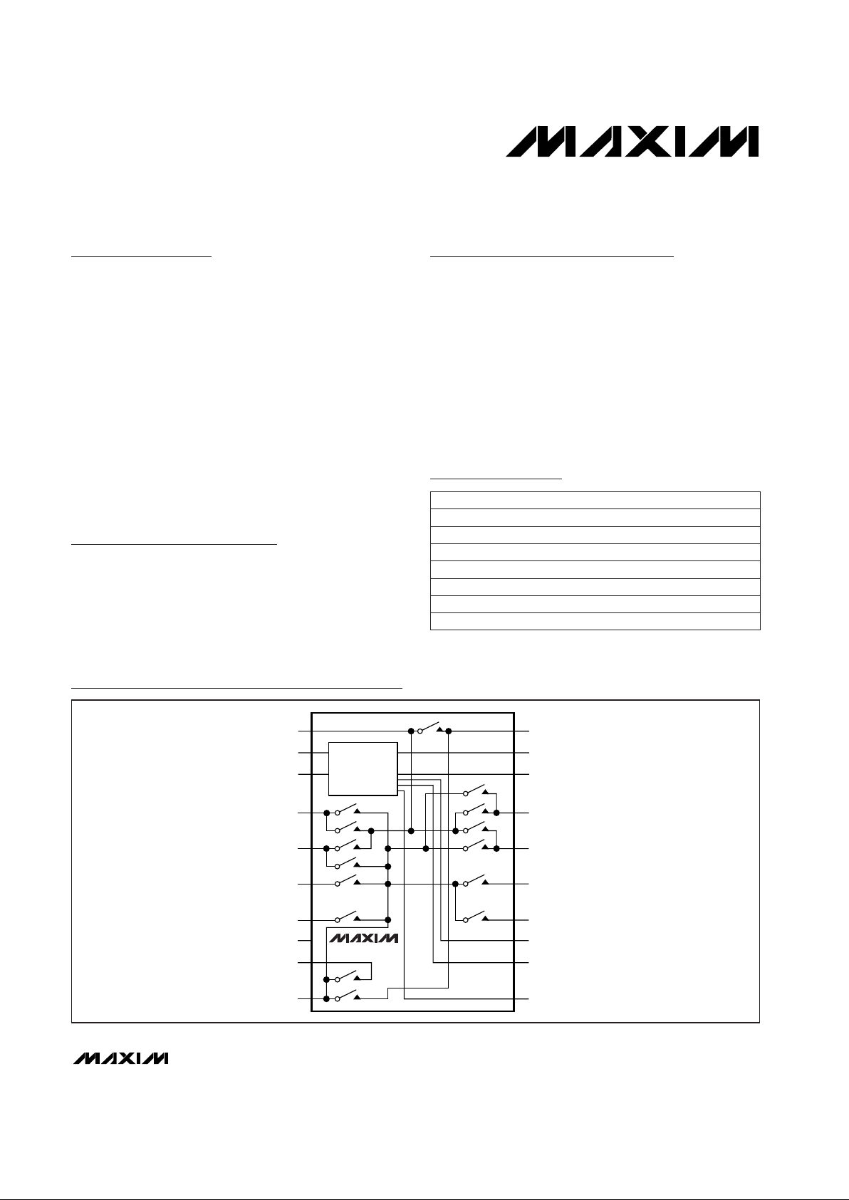
20
19
18
17
16
15
14
13
1
2
3
4
5
6
7
8
12
11
9
10
GND
A2
A3
NO8
NO6
NO7
NO5
EN
LATCH
NLATCH
NO4
AO
A1
COMB
V-
NO1
NO3
NO2
COMA
V+
MAX4598
LOGIC DECODER
19-1385; Rev 0; 10/98
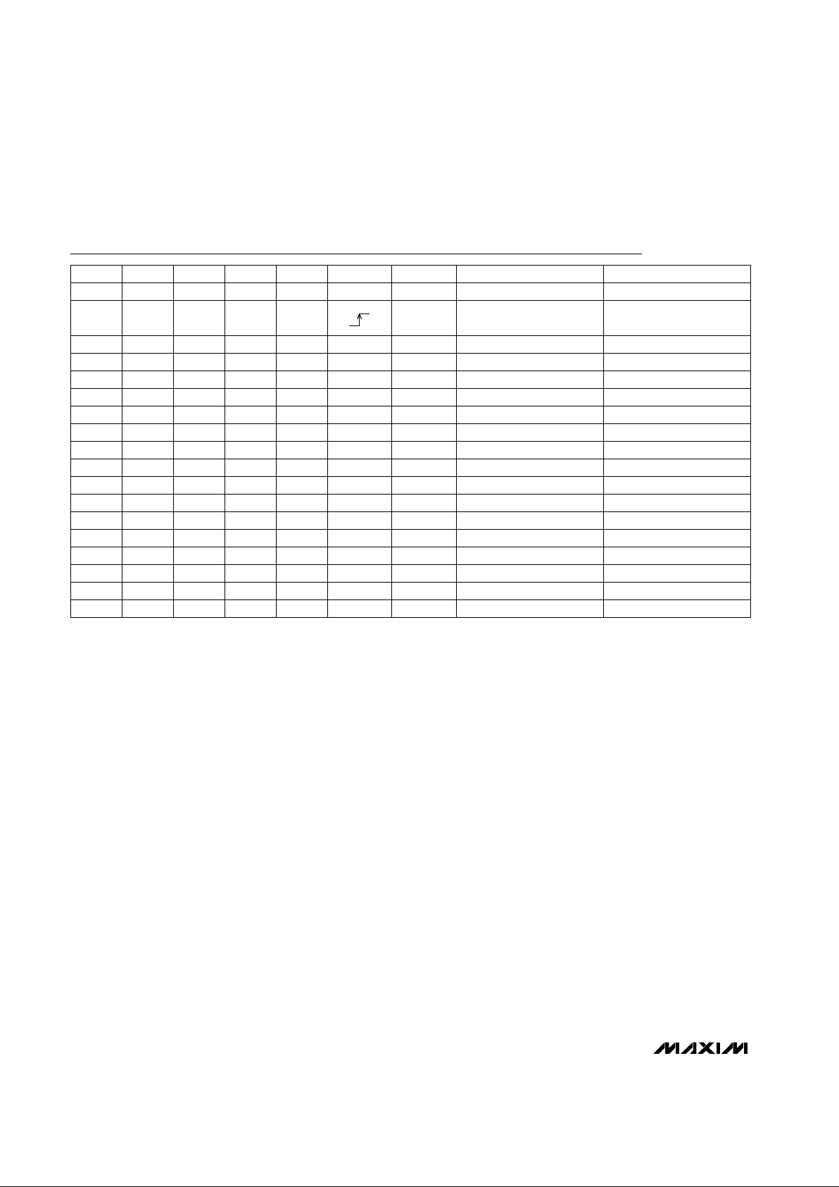
PART
MAX4598CAP
MAX4598CWP
MAX4598CCP 0°C to +70°C
0°C to +70°C
0°C to +70°C
TEMP. RANGE PIN-PACKAGE
20 SSOP
20 Wide SO
20 Plastic DIP
*
Contact factory for dice specifications.
Pin Configuration/Functional Diagram
Ordering Information
MAX4598C/D
MAX4598EAP -40°C to +85°C
0°C to +70°C Dice*
20 SSOP
MAX4598EWP
MAX4598EPP -40°C to +85°C
-40°C to +85°C 20 Wide SO
20 Plastic DIP
Rail-to-Rail is a registered trademark of Nippon Motorola, Ltd.
MAX4598
Low-Voltage, Combination Single-Ended
8-to-1/Differential 4-to-1 Multiplexer
2 _______________________________________________________________________________________
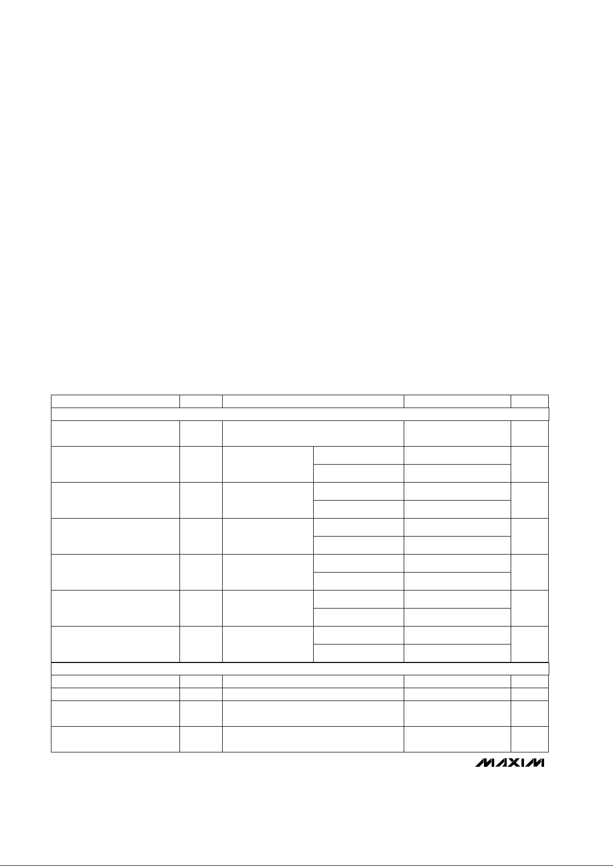
ABSOLUTE MAXIMUM RATINGS
ELECTRICAL CHARACTERISTICS—Dual Supplies
(V+ = +5V ±10%, V- = -5V ±10%, VIH= 2.4V, VIL= 0.8V, TA= T
MIN
to T
MAX
, unless otherwise noted. Typical values are at
T
A
= +25°C.) (Note 2)
Stresses beyond those listed under “Absolute Maximum Ratings” may cause permanent damage to the device. These are stress ratings only, and functional
operation of the device at these or any other conditions beyond those indicated in the operational sections of the specifications is not implied. Exposure to
absolute maximum rating conditions for extended periods may affect device reliability.
V+ to GND..............................................................-0.3V to +13V
V- to GND...............................................................-13V to +0.3V
V+ to V-...................................................................-0.3V to +13V
A_, EN, LATCH, NLATCH, NO_, COM_
(Note 1)...............................................(V- - 0.3V) to (V+ + 0.3V)
Continuous Current (any terminal)....................................±20mA
Peak Current, NO_, or COM_
(pulsed at 1ms, 10% duty cycle max)............................±40mA
Continuous Power Dissipation (TA= +70°C)
SSOP (derate 8mW/°C above +70°C) .........................640mW
Wide SO (derate 10mW/°C above +70°C)...................800mW
Plastic DIP (derate 10.53mW/°C above +70°C) ..........889mW
Operating Temperature Ranges
MAX4598C_P......................................................0°C to +70°C
MAX4598E_P...................................................-40°C to +85°C
Storage Temperature Range.............................-65°C to +160°C
Lead Temperature (soldering, 10sec).............................+300°C
Note 1: Signals on NO_, COM_, EN, LATCH, NLATCH, or A_ exceeding V+ or V- are clamped by internal diodes. Limit forward cur-
rent to maximum current ratings
I
COM_
= 1mA,
V
NO_
= ±3.0V,
V+ = 4.5V, V- = -4.5V
(Note 3)
VEN= VA_= V
LATCH
= V
NLATCH
= V
CAL
= V+
VNO_ = ±4.5V,
V
COM_
= ±4.5V,
V+ = 5.5V, V- = -5.5V
V
COM_
= ±4.5V,
V
NO_
= ±4.5V,
V+ = 5.5V, V- = -5.5V
I
COM_
= 1mA;
V
NO_
= -3V, 0, 3V;
V+ = 4.5V, V- = -4.5V
I
COM_
= 1mA,
V
NO_
= ±3.0V,
V+ = 4.5V, V- = -4.5V
V
COM_
= ±4.5V,
V
NO_
= ±4.5V,
V+ = 5.5V, V- = -5.5V
CONDITIONS
µA-0.1 0.01 0.1I
IH
Input Current with Input
Voltage High
V1.4 0.8V
IL
Input Low Voltage
V2.4 1.7V
IH
Input High Voltage
-10 10
nA
-0.2 0.01 0.2
I
COM(ON)
COM On-Leakage Current
(Note 6)
-10 10
Ω
45 75
R
ON
On-Resistance
VV- V+
V
COM_
,
V
NO_
Analog Signal Range
nA
-0.2 0.01 0.2
I
COM(OFF)
COM Off-Leakage Current
(Note 6)
-2 2
nA
-0.1 0.01 0.1
I
NO(OFF)
NO Off-Leakage Current
(Note 6)
13
Ω
1 4
∆R
ON
6
On-Resistance Matching
Between Channels (Note 4)
Ω
7 10
R
FLAT
On-Resistance Flatness
(Note 5)
UNITMIN TYP MAXSYMBOLPARAMETER
TA= +25°C
TA= +25°C
TA= T
MIN
to T
MAX
TA= T
MIN
to T
MAX
TA= +25°C
TA= T
MIN
to T
MAX
TA= +25°C
TA= T
MIN
to T
MAX
TA= +25°C
TA= +25°C
TA= T
MIN
to T
MAX
100TA= T
MIN
to T
MAX
VEN= VA_= V
LATCH
= V
NLATCH
= V
CAL
= 0 µA-0.1 0.01 0.1I
IL
Input Current with Input
Voltage Low
±
±
SWITCH
LOGIC INPUTS
MAX4598
Low-Voltage, Combination Single-Ended
8-to-1/Differential 4-to-1 Multiplexer
_______________________________________________________________________________________ 3
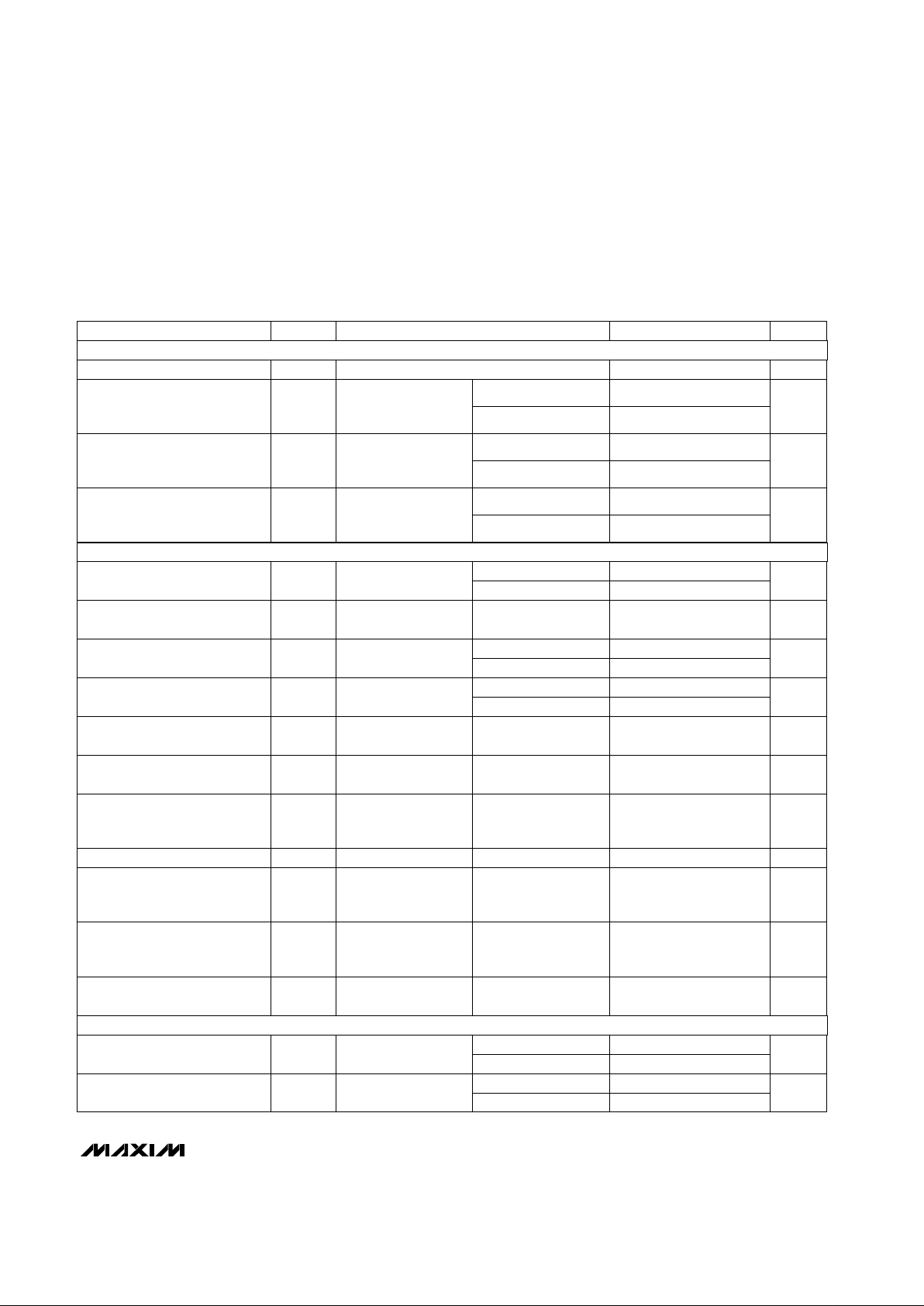
ELECTRICAL CHARACTERISTICS—Dual Supplies (continued)
(V+ = +5V ±10%, V- = -5V ±10%, VIH= 2.4V, VIL= 0.8V, TA= T
MIN
to T
MAX
, unless otherwise noted. Typical values are at
T
A
= +25°C.) (Note 2)
TA= +25°C
TA= +25°C
TA= +25°C
TA= T
MIN
to T
MAX
TA= +25°C
TA= +25°C
TA= T
MIN
to T
MAX
TA= +25°C
TA= +25°C
TA= T
MIN
to T
MAX
TA= +25°C
TA= +25°C
TA= T
MIN
to T
MAX
TA= +25°C
TA= +25°C
TA= T
MIN
to T
MAX
TA= T
MIN
to T
MAX
TA= +25°C
TA= T
MIN
to T
MAX
TA= +25°C
TA= T
MIN
to T
MAX
TA= +25°C
Break-Before-Make Interval
(Note 3)
t
OPEN
4 10 ns
150
Transition Time t
TRANS
65 100
ns
Enable Turn-On Time t
ON
55 90
ns
120
Enable Turn-Off Time t
OFF
40 70
ns
100
GND Supply Current
-5 5
I
GND
-1 0.001 1
µA
-5 5
Charge Injection (Note 3) V
CTE
2 5 pC
Off-Isolation (Note 7) V
ISO
-90 dB
Logic Input Capacitance C
IN
3 pF
COM Off-Capacitance
C
COM(OFF)
15 pF
COM On-Capacitance C
COM(ON)
26 pF
Setup Time t
S
30 70
ns
80
Hold Time t
H
-10 0
ns
-10
CL= 1nF, V
NO_
= 0,
Figure 4
Figure 2
VEN= 0, f = 1MHz,
Figure 5
Figure 1
Figure 3
f = 1MHz
Figure 3
f = 1MHz,
VEN= V
COM_
= 0,
Figure 6
f = 1MHz, VEN= 2.4V,
V
COM_
= 0
VEN= VA_= V
LATCH
= V
NLATCH
= 0 or V+,
V+ = 5.5V, V- = -5.5V
Figure 7
VEN= VA_= V
LATCH
= V
NLATCH
= 0 or V+,
V+ = 5.5V, V- = -5.5V
Figure 7
PARAMETER SYMBOL MIN TYP MAX UNIT
Power-Supply Range ±2.7 ±6 V
Positive Supply Current I+
-1 0.001 1
µA
-5 5
Negative Supply Current I-
-1 0.001 1
µA
CONDITIONS
TA= +25°CNO Off-Capacitance C
OFF
3 pF
f = 1MHz,
VEN= V
COM_
= 0,
Figure 6
VEN= VA_= V
LATCH
= V
NLATCH
= 0 or V+,
V+ = 5.5V, V- = -5.5V
Crosstalk Between Channels
(Note 8)
TA= +25°CV
CT
-80 dB
VEN= 2.4V, f = 1MHz,
V
GEN
= 1Vp-p,
Figure 5
SUPPLY
DYNAMIC
LATCH TIMING (Note 3)
CONDITIONS
MAX4598
Low-Voltage, Combination Single-Ended
8-to-1/Differential 4-to-1 Multiplexer
4 _______________________________________________________________________________________
V
NO_
= 3V,
Figure 1
VEN= VA_= V
LATCH
= V
NLATCH
= 0 or V+,
V+ = 5.5V
I
COM_
= 1mA,
V
NO_
= 3.0V,
V+ = 4.5V
(Note 3)
VEN= V
LATCH
= VA_= V
NLATCH
= 0
V
COM_
= 4.5V, 1V;
V
NO_
= 1V,4.5V;
V+ = 5.5V
V
NO_
= 4.5V, 1V;
V
COM_
= 1V, 4.5V;
V+ = 5.5V
I
COM_
= 1mA,
V
NO_
= 3.0V,
V+ = 4.5V
I
COM_
= 1mA;
V
NO_
= 3V, 2V, 1V;
V+ = 4.5V
V
COM_
= 4.5V,
V
NO_
= 4.5V,
V+ = 5.5V
CONDITIONS
ns
115 160
t
TRANS
Transition Time
-5 5
µA
-1 1
I+Positive Supply Current (Note 3)
V2.7 12.0Power-Supply Range
µA-0.1 0.01 0.1
Input Current with Input Voltage
Low
µA-0.1 0.01 0.1
Input Current with Input Voltage
High
V1.3 0.8V
IL
Input Low Voltage
V2.4 1.6V
IH
Input High Voltage
nA
-10 10
-0.2 0.2
I
COM(ON)
COM On-Leakage Current
(Notes 6, 9)
Ω
80 150
R
ON
On-Resistance
V0 V+
V
NO_
,
V
COM_
Analog Signal Range
nA
-10 10
-0.2 0.2
I
COM(OFF)
COM Off-Leakage Current
(Notes 6, 9)
-2 2
nA
-0.1 0.1
I
NO(OFF)
NO Off-Leakage Current
(Notes 6, 9)
200
Ω
2 8
∆R
ON
12
On-Resistance Matching
Between Channels (Notes 3, 4)
Ω8R
FLAT
On-Resistance Flatness
UNITMIN TYP MAXSYMBOLPARAMETER
Figure 3
Figure 2
Figure 3
ns
85 140
t
ON
Enable Turn-On Time
ns4 10t
OPEN
210
Break-Before-Make Interval
170
ns
60 100
t
OFF
Enable Turn-Off Time
120
TA= +25°C
TA= T
MIN
to T
MAX
TA= +25°C
TA= +25°C
TA= T
MIN
to T
MAX
TA= +25°C
TA= T
MIN
to T
MAX
TA= +25°C
TA= T
MIN
to T
MAX
TA= +25°C
TA= T
MIN
to T
MAX
TA= T
MIN
to T
MAX
TA= +25°C
TA= +25°C
TA= +25°C
TA= +25°C
TA= T
MIN
to T
MAX
TA= T
MIN
to T
MAX
TA= +25°C
TA= T
MIN
to T
MAX
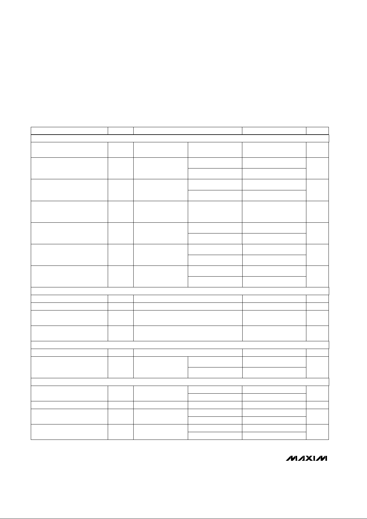
ELECTRICAL CHARACTERISTICS—Single +5V Supply
(V+ = +5V ±10%, V- = 0, VIH= 2.4V, VIL= 0.8V, TA= T
MIN
to T
MAX
, unless otherwise noted. Typical values are at TA= +25°C.)
(Note 2)
VEN= V
LATCH
= VA_= V
NLATCH
= V+
SWITCH
SUPPLY
LOGIC INPUTS (Note 3)
DYNAMIC (Note 3)

MAX4598
Low-Voltage, Combination Single-Ended
8-to-1/Differential 4-to-1 Multiplexer
_______________________________________________________________________________________ 5
I
COM_
= 0.2mA,
V
NO_
= 1.5V,
V+ = 2.7V
(Note 3)
V
NO1
= 1.5V,
Figure 3
V
NO1
= 1.5V,
Figure 3
Figure 7
V
NO1
= 1.5V,
V
NO8
= 0, Figure 1
Figure 7
CONDITIONS
ns-10 0t
H
Hold Time
ns45 80t
S
Setup Time
Ω
220 500
R
ON
On-Resistance
V0 V+Analog Signal Range
ns120 180t
OFF
Enable Turn-Off Time
ns160 250t
ON
Enable Turn-On Time
ns200 310t
TRANS
Transition Time
600
V2.4 1.1I
IH
Input High Voltage
V1.0 0.6I
IL
Input Low Voltage
UNITMIN TYP MAXSYMBOLPARAMETER
TA= +25°C
TA= +25°C
TA= +25°C
TA= +25°C
TA= +25°C
TA= T
MIN
to T
MAX
TA= +25°C
CONDITIONS
ELECTRICAL CHARACTERISTICS—Single +5V Supply (continued)
(V+ = +5V ±10%, V- = 0, VIH= 2.4V, VIL= 0.8V, TA= T
MIN
to T
MAX
, unless otherwise noted. Typical values are at TA= +25°C.)
(Note 2)
ELECTRICAL CHARACTERISTICS—Single +3V Supply
(V+ = +2.7V to +3.6V, V- = 0, VIH= 2.4V, VIL= 0.6V, TA= T
MIN
to T
MAX
, unless otherwise noted. Typical values are at TA= +25°C.)
CONDITIONS UNITMIN TYP MAXSYMBOLPARAMETER
Figure 7
Figure 7
CL= 1nF, V
NO_
= 0,
Figure 4
-10
ns
-10 0
t
H
Hold Time
80
ns
30 70
t
S
Setup Time
pC1 5V
CTE
Charge Injection
CONDITIONS
TA= +25°C
TA= T
MIN
to T
MAX
TA= +25°C
TA= +25°C
TA= T
MIN
to T
MAX
Note 2: The algebraic convention, where the most negative value is a minimum and the most positive value a maximum, is used in
this data sheet.
Note 3: Guaranteed by design.
Note 4: ∆R
ON
= R
ON(MAX)
- R
ON(MIN)
.
Note 5: Flatness is defined as the difference between the maximum and minimum value of on-resistance as measured over the
specified analog signal range.
Note 6: Leakage parameters are 100% tested at maximum-rated hot temperature and guaranteed by correlation at +25°C.
Note 7: Off-Isolation = 20log
10(VCOM
/ VNO), V
COM
= output, VNO= input to off switch.
Note 8: Between any two switches.
Note 9: Leakage testing at single supply is guaranteed by testing with dual supplies.
LATCH TIMING (Note 3)
CONDITIONS
LOGIC INPUTS (Note 3)
SWITCH
DYNAMIC (Note 3)
LATCH TIMING (Note 3)
LOGIC INPUTS (Note 3)
CONDITIONS

MAX4598
Low-Voltage, Combination Single-Ended
8-to-1/Differential 4-to-1 Multiplexer
6 _______________________________________________________________________________________
Typical Operating Characteristics
(TA = +25°C, unless otherwise noted.)
0
30
20
10
40
50
60
-5 -1-2-4 -3 0 1 2 3 4 5
ON-RESISTANCE vs. V
COM
AND
TEMPERATURE (DUAL SUPPLIES)
MAX4598-01
V
COM
(V)
R
ON
(Ω)
V+ = +5V
V- = -5V
TA = +85°C
TA = +25°C
TA = -40°C
TA = +70°C
0
40
50
30
20
10
60
70
80
90
0 2.01.50.5 1.0 2.5 3.0 3.5 4.0 4.5 5.0
ON-RESISTANCE vs. V
COM
AND
TEMPERATURE (SINGLE SUPPLY)
MAX4598-02
V
COM
(V)
R
ON
(Ω)
V+ = +5V
V- = 0
TA = +25°C
TA = -40°C
TA = +85°C
TA = +70°C
30
110
90
70
50
130
150
170
190
0 2.01.50.5 1.0 2.5 3.0 3.5 4.0 4.5 5.0
ON-RESISTANCE vs. V
COM
(SINGLE SUPPLY)
MAX4598-03
V
COM
(V)
R
ON
(Ω)
V+ = +2.7V
V+ = +3V
V+ = +5V
30
70
60
50
40
80
90
100
110
-5 -1-2-4 -3 0 1 2 3 4 5
ON-RESISTANCE vs. V
COM
(DUAL SUPPLIES)
MAX4598-04
V
COM
(V)
R
ON
(Ω)
V+ = +2.7V
V- = -2.7V
V+ = +3V
V- = -3V
V+ = +5V
V- = -5V
20
50
40
30
60
70
80
-40 0 25 70 85
TURN-ON/TURN-OFF TIMES
vs. TEMPERATURE
MAX4598-07
TEMPERATURE (°C)
t
ON
, t
OFF
(ns)
V+ = +5V
V- = -5V
t
ON
t
OFF
100n
10f
-40 -20 0 20 40 60 80 100 120
LEAKAGE CURRENT
vs. TEMPERATURE
100f
1p
MAX4598-05
TEMPERATURE (°C)
LEAKAGE CURRENT (A)
10p
100p
10n
1n
COM (ON)
COM (OFF)
NO (OFF)
1f
10p
100p
1p
100f
10f
1n
10n
100n
1000n
-40 20-20 0 40 60 80
100
120 140
SUPPLY CURRENT vs. TEMPERATURE
MAX4598-06
TEMPERATURE (°C)
SUPPLY CURRENT (A)
V+ = +5V
V- = -5V
I+
I-
0
80
60
20
40
100
120
140
2 3 4 5
TURN-ON/TURN-OFF TIMES
vs. SUPPLY VOLTAGE (DUAL SUPPLIES)
MAX4598-08
V+, V- (V)
t
ON
, t
OFF
(ns)
t
ON
t
OFF

_______________Detailed Description
The MAX4598 can be configured as a single 8-channel
or dual 4-channel multiplexer. In the single 8-to-1 multiplexer configuration, COMA connects to one of the
eight inputs (NO1 to NO8), GND, or V+ by the address
inputs A0 to A2 (see
Truth Table
). In the dual 4-to-1
multiplexer configuration, COMA connects to one of the
four inputs (NO1, NO3, NO5, NO7), GND, or V+, and
COMB connects to one of the four inputs (NO2, NO4,
NO6, NO8) or GND by the address inputs A0 to A2
(see
Truth Table
).
The MAX4598 functions as a standard multiplexer
when NLATCH is high. When NLATCH is low, the condition set by A0 to A3 is activated at the rising edge of
LATCH. Otherwise, the outputs remain at the previously
set condition.
__________Applications Information
The MAX4598 construction is typical of most CMOS
analog switches. It has three supply pins: V+, V-, and
GND. The positive and negative power supplies are
used to drive the internal CMOS switches and set the
limits of the analog voltage on any switch. Reverse
ESD-protection diodes are internally connected between each analog signal pin and V+ and V-. If the voltage on any pin exceeds V+ or V- by 0.3V, one of the
ESD diodes starts to conduct. During normal operation
these reverse-biased ESD diodes leak, forming the only
current drawn from V-.
MAX4598
Low-Voltage, Combination Single-Ended
8-to-1/Differential 4-to-1 Multiplexer
_______________________________________________________________________________________ 7
-2
2
1
0
-1
4
3
5
6
-5 -1-2-4 -3 0 1 2 3 4 5
CHARGE INJECTION vs. V
COM
MAX4598-10
V
COM
(V)
Q (pC)
V+ = +5V
V- = -5V
V+ = +5V
V- = 0
Typical Operating Characteristics (continued)
(TA = +25°C, unless otherwise noted.)
Pin Description
Positive Supply VoltageV+9
Multiplexer Output ACOMA10
Data-Strobe Mode SelectNLATCH11
Latch InputLATCH12
Multiplexer EnableEN13
Channel Input 2NO25
Channel Input 3NO36
Channel Input 1NO17
Negative Supply VoltageV-8
Channel Input 4NO44
Address Bit 0A03
PIN
Address Bit 1A12
Multiplexer Output BCOMB1
FUNCTIONNAME
Channel Input 6NO616
Channel Input 8NO817
Address Bit 3A318
Address Bit 2A219
GroundGND20
Channel Input 5NO514
Channel Input 7NO715
0
-90
0.1 10 1001 1000
FREQUENCY RESPONSE
-70
-80
MAX4598-09
FREQUENCY (MHz)
LOSS (dB)
-50
-60
-40
-30
-10
-20
180
-180
-100
-140
PHASE (°C)
-20
-60
20
60
140
100
OFF-ISOLATION
INSERTION LOSS
ON-PHASE
MAX4598
Low-Voltage, Combination Single-Ended
8-to-1/Differential 4-to-1 Multiplexer
8 _______________________________________________________________________________________
Truth Table
NO7x0
NO8x0
NO1x1
NO3x1
NO5x1
NO3x0
NO4x0
NO5x0
NO6x0
NO2x0
NO1x0
A3
State is latched on the
rising edge of LATCH
x
High-Zxx
COMALATCH
V+x1
NO8x1
High-Zx1
NO7x1
GNDx1
1
1
0
0
0
0
0
1
1
0
0
A2
x
x
1
1
1
0
1
1
1
0
0
1
1
1
0
0
0
0
A1
x
x
0
1
1
0
1
0
1
0
1
0
0
1
0
1
1
0
A0
x
x
1
0
1
1
0
1
1
1
1
1
1
1
1
1
1
1
EN
1
0
1
1
1
1
1
1
1
1
1
1
1
1
1
1
1
1
0
x
NLATCH
1
1
1
1
1
GND
GND
NO2
NO4
NO6
GND
GND
GND
GND
GND
GND
State is latched on the
rising edge of LATCH
High-Z
COMB
GND
NO8
High-Z
NO8
GND
x = Don’t care
Virtually all the analog leakage current is through the
ESD diodes. Although the ESD diodes on a given signal pin are identical, and therefore fairly well balanced,
they are reverse-biased differently. Each is biased by
either V+ or V- and the analog signal. This means their
leakage varies as the signal varies. The difference in
the two diodes’ leakage from the signal path to the V+
and V- pins constitutes the analog signal-path leakage
current. All analog leakage current flows to the supply
terminals, not to the other switch terminal. This explains
how both sides of a given switch can show leakage
currents of either the same or opposite polarity.
There is no connection between the analog signal
paths and GND. The analog signal paths consist of an
N-channel and a P-channel MOSFET, with their sources
and drains paralleled and their gates driven out of
phase with V+ and V- by the logic-level translators.
V+ and GND power the internal logic and logic-level
translators, and set the input logic thresholds. The
logic-level translators convert the logic levels to
switched V+ and V- signals to drive the analog switch
gates. This drive signal is the only connection between
the logic supplies and the analog supplies. All pins
have ESD protection to V+ and to V-.
Increasing V- has no effect on the logic-level thresholds, but it does increase the drive to the P-channel
switches, reducing their on-resistance. V- also sets the
negative limit of the analog signal voltage.
The logic-level thresholds are CMOS- and TTL-compatible when V+ is +5V. As V+ is raised, the threshold
increases slightly; when V+ reaches +12V, the level
threshold is about 3.2V, which is above the TTL output
high-level minimum of 2.4V but still compatible with
CMOS outputs.
Bipolar-Supply Operation
The MAX4598 operates with bipolar supplies between
±2.7V and ±6V. The V+ and V- supplies need not be
symmetrical, but their sum cannot exceed the absolute
maximum rating of 13V. Do not connect the MAX4598
V+ pin to +3V and connect the logic-level input pins
to TTL logic-level signals. TTL logic-level outputs
can exceed the absolute maximum ratings, causing
damage to the part and/or external circuits.

Caution: The absolute maximum V+ to V- differential
voltage is 13V. Typical “±6 Volt” or “12 Volt” supplies with ±10% tolerances can be as high as 13.2V
from V+ to V-. This voltage can damage the
MAX4598. Even ±5% tolerance supplies may have
overshoot or noise spikes that exceed 13V.
Single-Supply Operation
The MAX4598 operates from a single supply between
+2.7V and +12V when V- is connected to GND. All of
the bipolar precautions must be observed. However,
these parts are optimized for ±5V operation, and most
AC and DC characteristics are degraded significantly
when departing from ±5V. As the overall supply voltage
(V+ to V-) is lowered, switching speed, on-resistance,
off-isolation, and distortion are degraded (see
Typical
Operating Characteristics
).
Single-supply operation also limits signal levels and
interferes with grounded signals. When V- = 0, AC signals are limited to -0.3V. Voltages below -0.3V can be
clipped by the internal ESD-protection diodes, and the
parts can be damaged if excessive current flows.
Power Off
When power to the MAX4598 is off (i.e., V+ = V- = 0),
the Absolute Maximum Ratings still apply: neither logiclevel inputs on NO_ nor signals on COM_ can exceed
±0.3V. Voltages beyond ±0.3V cause the internal ESDprotection diodes to conduct, and the parts can be
damaged if excessive current flows.
MAX4598
Low-Voltage, Combination Single-Ended
8-to-1/Differential 4-to-1 Multiplexer
_______________________________________________________________________________________ 9
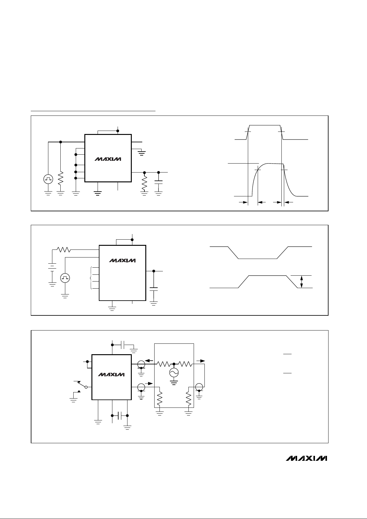
Test Circuits/Timing Diagrams
50%
50%
t
R
< 20ns
t
F
< 20ns
V
OUT
V+
0V
V
NO1
0V
V
NO8
LOGIC
INPUT
V
EN
SWITCH
OUTPUT
V+
A1
A2
A0
+5V
V
OUT
-5V
GND
V+
V-
EN
NLATCH
NO1
NO2–NO7
NO8
COMA
+3V
50Ω
MAX4598
300Ω
35pF
90%
90%
t
TRANS
t
TRANS
-3V
LATCH
A3
Figure 1. Transition Time
50% 50%
t
OPEN
tR < 20ns
tF < 20ns
V
OUT
V+
0V
LOGIC
INPUT
V
A
SWITCH
OUTPUT
V
COM
+5V
V
OUT
-5V
GND
V+NLATCH
V-
A0
A1
A2
EN
NO1–NO8
COMA
+3V
50Ω
MAX4598
300Ω
35pF
90%
0V
V
A
LATCH
A3
Figure 2. Break-Before-Make Interval
MAX4598
Low-Voltage, Combination Single-Ended
8-to-1/Differential 4-to-1 Multiplexer
10 ______________________________________________________________________________________
Test Circuits/Timing Diagrams (continued)
50%
50%
t
OFF
tR < 20ns
t
F
< 20ns
V+
0V
0V
V
EN
V
OUT
+5V
V
OUT
-5V
GND
V+
NLATCH
A1
V-
A0
EN
LATCH
A3
NO1
NO2–NO8
COMA
+3V
50Ω
MAX4598
1k
35pF
A2
90%90%
t
ON
V
EN
Figure 3. Enable Switching Time
∆V
OUT
V+
0V
LOGIC
INPUT
V
EN
+5V
V
COM
-5V
GND
V+NLATCH
A1
V-
A0
EN
COMA
MAX4598
CL
1nF
V
COM
NO
CHANNEL
SELECT
R
S
V
S
OFFON ON
∆V
OUT
IS THE MEASURED VOLTAGE DUE TO CHARGE TRANSFER
ERROR Q WHEN THE CHANNEL TURNS OFF.
Q = (∆V
OUT
) (CL)
A2
A3
V
EN
Figure 4. Charge Injection
MEASUREMENTS ARE STANDARDIZED AGAINST SHORT AT SOCKET TERMINALS.
OFF-ISOLATION IS MEASURED BETWEEN COM AND “OFF” TERMINAL ON EACH SWITCH.
ON LOSS IS MEASURED BETWEEN COM AND “ON” TERMINAL ON EACH SWITCH.
NOTES:
+5V
V+
V+
V
OUT
GND
V-
LATCH
-5V
10nF
V-
A_
EN
NLATCH
NO_
COM_
V
IN
MAX4598
OFF-ISOLATION = 20log
V
OUT
V
IN
CROSSTALK = 20log
V
OUT
V
IN
NETWORK
ANALYZER
50Ω
50Ω 50Ω
50Ω
MEAS. REF
10nF
Figure 5. Off-Isolation/Crosstalk

MAX4598
Low-Voltage, Combination Single-Ended
8-to-1/Differential 4-to-1 Multiplexer
______________________________________________________________________________________ 11
Test Circuits/Timing Diagrams
(continued)
GND
LATCH,
EN
+5V
-5V
V+NLATCH
A3
V-
A2
A1
NO8
MAX4598
A0
CHANNEL
SELECT
NO1
COM_
1MHz
CAPACITANCE
ANALYZER
Figure 6. NO_/COM_ Capacitance
LATCH
V
IH
V
IL
ADDRESS
NOTE: TIMING MEASUREMENT REFERENCE LEVEL IS
V
IH
- V
IL
2
t
S
t
H
50%
+5V
-5V
GND
V+
V-
A1
A2
A3
EN
+3V
COM
LATCH
A0
MAX4598
NO2
NO1, NO3–NO8
NLATCH
Figure 7. Setup Time, Hold Time
TRANSISTOR COUNT: 287
SUBSTRATE CONNECTED TO V+
____________________Chip Topography
NO8
NO6
NO7
NO5
A0
A1
COMB
GND A2
A3
0.104"
(2.64mm)
0.092"
(2.34mm)
V-
V+
NO4
NO2
NO1
NO3
COMA
LATCH EN
NLATCH

MAX4598
Low-Voltage, Combination Single-Ended
8-to-1/Differential 4-to-1 Multiplexer
Maxim cannot assume responsibility for use of any circuitry other than circuitry entirely embodied in a Maxim product. No circuit patent licenses are
implied. Maxim reserves the right to change the circuitry and specifications without notice at any time.
12
____________________Maxim Integrated Products, 120 San Gabriel Drive, Sunnyvale, CA 94086 408-737-7600
© 1998 Maxim Integrated Products Printed USA is a registered trademark of Maxim Integrated Products.
NOTES
 Loading...